Revised January 2005
74VCX16722
Low Voltage 22-Bit Register
with 3.6V Tolerant Inputs and Outputs
General Description
Features
The VCX16722 low voltage 22-bit register contains twentytwo non-inverting D-type flip-flops with 3-STATE outputs
and is intended for bus oriented applications. The design
has been optimized for use with JEDEC compliant 200 pin
DIMM modules.
■ 1.65V–3.6V VCC supply operation
The 74VCX16722 is designed for low voltage (1.65V to
3.6V) VCC applications with I/O capability up to 3.6V.
The 74VCX16722 is fabricated with an advanced CMOS
technology to achieve high speed operation while maintaining low CMOS power dissipation.
■ 3.6V tolerant inputs and outputs
■ tPD (CLK to O n)
3.6ns max for 3.0V to 3.6V VCC
4.6ns max for 2.3V to 2.7V VCC
9.2ns max for 1.65V to 1.95V VCC
■ Power-down high impedance inputs and outputs
■ Supports live insertion/withdrawal (Note 1)
■ Meets JEDEC registered module specifications
■ Static Drive (IOH/IOL)
±24mA @ 3.0V
±18mA @ 2.3V
±6mA @ 1.65V
■ Latchup performance exceeds 300 mA
■ ESD performance:
Human body model > 2000V
Machine model >200V
Note 1: To ensure the high-impedance state during power up or power
down, OE should be tied to VCC through a pull-up resistor; the minimum
value of the resistor is determined by the current sourcing capability of the
driver.
Ordering Code:
Order Number
Package Number
Package Description
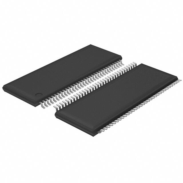
74VCX16722MTD
MTD64
64-Lead Thin Shrink Small Outline Package (TSSOP), JEDEC MO-153, 6.1mm Wide
Devices also available in Tape and Reel. Specify by appending the suffix letter “X” to the ordering code.
© 2005 Fairchild Semiconductor Corporation
DS500192
www.fairchildsemi.com
74VCX16722 Low Voltage 22-Bit Register with 3.6V Tolerant Inputs and Outputs
February 1999
�74VCX16722
Connection Diagram
Pin Descriptions
Pin Names
Description
OE
Output Enable Input (Active LOW)
CE
Clock Enable Input (Active Low)
CLK
Clock Input
D0- D21
Data Inputs
O0 - O21
3-STATE Outputs
Truth Table
CLK
CE
OE
Dn
On
X
X
H
X
Z
X
H
L
X
On
↑
L
L
L
L
↑
L
L
H
H
L or H
L
L
X
On
H = Logic HIGH
L = Logic LOW
X = Don’t Care, but not floating
Z = High Impedance
On = Previous On before LOW-to-HIGH Clock Transition
↑ = LOW-to-HIGH Clock Transition
Functional Description
Logic Diagram
The VCX16722 contains twenty-two D-type flip-flops with
3-STATE standard outputs. The twenty-two flip-flops will
store the state of their individual D-type inputs that meet
the setup and hold time requirements on the LOW-HIGH
Clock (CLK) transition, when the Clock-Enable (CE) is
LOW. The 3-STATE standard outputs are controlled by the
Output-Enable (OE). When OE is HIGH, the standard outputs are in high impedance mode but this does not interfere with entering new data into the flip-flops.
www.fairchildsemi.com
2
�Supply Voltage (VCC)
−0.5V to +4.6V
DC Input Voltage (VI)
−0.5V to +4.6V
Recommended Operating
Conditions (Note 4)
Power Supply
Output Voltage (VO)
Operating
Outputs 3-STATE
−0.5V to +4.6V
Outputs Active (Note 3)
−0.5V to VCC +
0.5V
DC Input Diode Current (IIK) VI < 0V
Output Voltage (VO)
DC Output Diode Current (IOK)
VO < 0V
−50 mA
+50 mA
±50 mA
Supply Pin (ICC or Ground)
0V to VCC
0V to 3.6V
VCC = 3.0V to 3.6V
±24 mA
VCC = 2.3V to 2.7V
±18 mA
VCC = 1.65V to 2.3V
DC VCC or Ground Current per
Storage Temperature Range (TSTG)
Output in Active States
Output in 3-STATE
Output Current in IOH/IOL
DC Output Source/Sink Current
(IOH/IOL)
1.2V to 3.6V
−0.3V to 3.6V
Input Voltage
−50 mA
VO > VCC
1.65V to 3.6V
Data Retention Only
±6 mA
Free Air Operating Temperature (TA)
±100 mA
−40°C to +85°C
Minimum Input Edge Rate (∆t/∆V)
−65°C to +150°C
VIN = 0.8V to 2.0V, VCC = 3.0V
10 ns/V
Note 2: The “Absolute Maximum Ratings” are those values beyond which
the safety of the device cannot be guaranteed. The device should not be
operated at these limits. The parametric values defined in the Electrical
Characteristics tables are not guaranteed at the Absolute Maximum Ratings. The Recommended Operating Conditions tables will define the conditions for actual device operation.
Note 3: IO Absolute Maximum Rating must be observed.
Note 4: Floating or unused pin (inputs or I/O's) must be held HIGH or LOW.
DC Electrical Characteristics (2.7V < VCC ≤ 3.6V)
Symbol
Parameter
Conditions
VCC
(V)
VIH
HIGH Level Input Voltage
2.7–3.6
VIL
LOW Level Input Voltage
2.7–3.6
VOH
HIGH Level Output Voltage
VOL
LOW Level Output Voltage
2.0
VCC − 0.2
IOH = −12 mA
2.7
2.2
IOH = −18 mA
3.0
2.4
IOH = −24 mA
3.0
2.2
IOL = 100 µA
2.7–3.6
0.2
IOL = 12 mA
2.7
0.4
IOL = 18 mA
3.0
0.4
IOL = 24 mA
0V ≤ VI ≤ 3.6V
IOZ
3-STATE Output Leakage
0V ≤ VO ≤ 3.6V
VI = V IH or VIL
IOFF
Power Off Leakage Current
0V ≤ (VI, VO) ≤ 3.6V
ICC
Quiescent Supply Current
VI = V CC or GND
VCC ≤ (VI, VO) ≤ 3.6V (Note 5)
VIH = VCC − 0.6V
Units
V
0.8
2.7–3.6
Input Leakage Current
Increase in ICC per Input
Max
IOH = −100 µA
II
∆ICC
Min
V
V
V
3.0
0.55
2.7–3.6
±5.0
µA
2.7–3.6
±10
µA
0
10
µA
2.7–3.6
2.7–3.6
20
±20
750
µA
µA
Note 5: Outputs disabled or 3-STATE only.
3
www.fairchildsemi.com
74VCX16722
Absolute Maximum Ratings(Note 2)
�74VCX16722
DC Electrical Characteristics (2.3V ≤ VCC ≤ 2.7V)
Symbol
Parameter
Conditions
VCC
(V)
VIH
HIGH Level Input Voltage
2.3–2.7
VIL
LOW Level Input Voltage
2.3–2.7
VOH
HIGH Level Output Voltage
VOL
LOW Level Output Voltage
IOH = −100 µA
2.3–2.7
Min
Max
Units
0.7
V
1.6
V
VCC − 0.2
IOH = −6 mA
2.3
2.0
IOH = −12 mA
2.3
1.8
IOH = −18 mA
2.3
1.7
V
IOL = 100 µA
2.3–2.7
0.2
IOL = 12mA
2.3
0.4
IOL = 18 mA
2.3
0.6
2.3–2.7
±5.0
µA
2.3–2.7
±10
µA
0
10
µA
II
Input Leakage Current
0 ≤ VI ≤ 3.6V
IOZ
3-STATE Output Leakage
0 ≤ VO ≤ 3.6V
VI = VIH or VIL
IOFF
Power Off Leakage Current
0 ≤ (VI, V O) ≤ 3.6V
ICC
Quiescent Supply Current
VI = VCC or GND
VCC ≤ (VI, VO) ≤ 3.6V (Note 6)
20
2.3–2.7
±20
V
µA
Note 6: Outputs disabled or 3-STATE only.
DC Electrical Characteristics (1.65V ≤ VCC < 2.3V)
Symbol
Parameter
Conditions
VCC
(V)
VIH
HIGH Level Input Voltage
1.65 - 2.3
VIL
LOW Level Input Voltage
1.65 - 2.3
VOH
HIGH Level Output Voltage
VOL
LOW Level Output Voltage
IOH = −100 µA
Max
0.65 × VCC
VCC − 0.2
IOH = −6 mA
1.65
1.25
IOL = 100 µA
1.65 - 2.3
0.2
1.65
0.3
II
Input Leakage Current
0 ≤ VI ≤ 3.6V
IOZ
3-STATE Output Leakage
0 ≤ VO ≤ 3.6V
VI = VIH or VIL
IOFF
Power Off Leakage Current
0 ≤ (VI, V O) ≤ 3.6V
ICC
Quiescent Supply Current
VI = VCC or GND
VCC ≤ (VI, VO) ≤ 3.6V (Note 7)
Note 7: Outputs disabled or 3-STATE only.
4
Units
V
0.35 × VCC
1.65 - 2.3
IOL = 6mA
www.fairchildsemi.com
Min
V
V
V
1.65 - 2.3
±5.0
µA
1.65 - 2.3
±10
µA
0
10
µA
1.65 - 2.3
20
±20
µA
�TA = −40°C to +85°C, CL = 30 pF, RL = 500Ω
Symbol
Parameter
VCC = 3.3V ± 0.3V
Min
VCC = 2.5 ± 0.2V
Max
Min
VCC = 1.8 ± 0.15V
Max
Min
200
Units
Max
fMAX
Maximum Clock Frequency
250
tPHL, tPLH
Propagation Delay Clock to Bus
1.3
3.6
1.5
4.6
100
2.0
9.2
ns
tPZL, tPZH
Output Enable Time
0.6
3.5
0.8
4.5
1.5
9.0
ns
tPLZ, tPHZ
Output Disable Time
0.6
3.2
0.8
4.2
1.5
7.6
tS
Setup Time
2.0
tH
Hold Time
0.0
0.0
0.5
ns
tW
Pulse Width
1.5
1.5
4.0
ns
tOSHL
Output to Output Skew
tOSLH
(Note 9)
2.0
0.5
MHz
3.0
ns
ns
0.5
0.75
ns
Note 8: For CL= 50 pF, add approximately 300 ps to the AC maximum specification.
Note 9: Skew is defined as the absolute value of the difference between the actual propagation delay for any two separate outputs of the same device. The
specification applies to any outputs switching in the same direction, either HIGH-to-LOW (tOSHL) or LOW-to-HIGH (tOSLH).
AC Electrical Characteristics Over Load (Note 10)
TA = −0°C to +70°C, RL = 500Ω VCC = 3.3V ± 0.3V
Symbol
CL = 0 pF
Parameter
Min
CL = 50 pF
Units
Max
Min
Max
tPHL, tPLH
Propagation Delay Clock to Bus
1.1
2.5
1.9
3.9
ns
tPZL, tPZH
Output Enable Time
0.7
2.4
1.0
3.8
ns
tPLZ, tPHZ
Output Disable Time
0.7
2.1
1.0
3.5
tS
Setup Time
2.0
tH
Hold Time
0.0
0.0
ns
tW
Pulse Width
1.5
1.5
ns
2.0
ns
ns
Note 10: This parameter is guaranteed by characterization but not tested.
Dynamic Switching Characteristics
Symbol
VOLP
VOLV
VOHV
Parameter
Quiet Output Dynamic Peak VOL
Quiet Output Dynamic Valley VOL
Quiet Output Dynamic Valley VOH
Conditions
CL = 30 pF, VIH = VCC, VIL = 0V
CL = 30 pF, VIH = VCC, VIL = 0V
CL = 30 pF, VIH = VCC, VIL = 0V
5
VCC
TA = +25°C
(V)
Typical
1.8
0.25
2.5
0.6
3.3
0.8
1.8
−0.25
2.5
−0.6
3.3
−0.8
1.8
1.5
2.5
1.9
3.3
2.2
Units
V
V
V
www.fairchildsemi.com
74VCX16722
AC Electrical Characteristics (Note 8)
�74VCX16722
Capacitance
Symbol
Parameter
Conditions
TA = +25°C
Typical
Units
CIN
Input Capacitance
VI = 0V or VCC, VCC = 1.8V, 2.5V, or 3.3V,
3.5
CI/O
Input/Output Capacitance
VI = 0V, or VCC, VCC = 1.8V, 2.5V or 3.3V
5.5
pF
CPD
Power Dissipation Capacitance
VI = 0V or VCC, f = 10 MHz, VCC = 1.8V, 2.5V or 3.3V
13
pF
IOUT - VOUT Characteristics
IOH versus VOH
FIGURE 1. Characteristics for Output - Pull Up Driver
IOL versus VOL
FIGURE 2. Characteristics for Output - Pull Down Driver
www.fairchildsemi.com
6
pF
�74VCX16722
AC Loading and Waveforms
FIGURE 3. AC Test Circuit
TEST
SWITCH
tPLH, tPHL
Open
tPZL, tPLZ
6V at VCC = 3.3 ± 0.3V;
VCC x 2 at VCC = 2.5 ± 0.2V; 1.8V to ± 0.15V
tPZH, tPHZ
GND
FIGURE 4. Waveform for Inverting and
Non-inverting Functions
tr = tf ≤ 2.0ns, 10% to 90%
FIGURE 5. 3-STATE Output High Enable and
Disable Times for Low Voltage Logic
tr = tf ≤ 2.0ns, 10% to 90%
FIGURE 6. 3-STATE Output Low Enable and Disable Times for Low Voltage Logic
tr = tf ≤ 2.0ns, 10% to 90%
Symbol
VCC
3.3V ± 0.3V
2.5V ± 0.2V
Vmi
1.5V
VCC/2
VCC/2
Vmo
1.5V
VCC/2
VCC/2
Vx
VOL + 0.3V
VOL + 0.15V
VOL + 0.15V
Vy
VOH − 0.3V
VOH − 0.15V
VOH − 0.15V
7
1.8 ± 0.15V
www.fairchildsemi.com
�74VCX16722 Low Voltage 22-Bit Register with 3.6V Tolerant Inputs and Outputs
Physical Dimensions inches (millimeters) unless otherwise noted
64-Lead Thin Shrink Small Outline Package (TSSOP), JEDEC MO-153, 6.1mm Wide
Package Number MTD64
Fairchild does not assume any responsibility for use of any circuitry described, no circuit patent licenses are implied and
Fairchild reserves the right at any time without notice to change said circuitry and specifications.
LIFE SUPPORT POLICY
FAIRCHILD’S PRODUCTS ARE NOT AUTHORIZED FOR USE AS CRITICAL COMPONENTS IN LIFE SUPPORT
DEVICES OR SYSTEMS WITHOUT THE EXPRESS WRITTEN APPROVAL OF THE PRESIDENT OF FAIRCHILD
SEMICONDUCTOR CORPORATION. As used herein:
2. A critical component in any component of a life support
device or system whose failure to perform can be reasonably expected to cause the failure of the life support
device or system, or to affect its safety or effectiveness.
1. Life support devices or systems are devices or systems
which, (a) are intended for surgical implant into the
body, or (b) support or sustain life, and (c) whose failure
to perform when properly used in accordance with
instructions for use provided in the labeling, can be reasonably expected to result in a significant injury to the
user.
www.fairchildsemi.com
www.fairchildsemi.com
8
�