Is Now Part of
To learn more about ON Semiconductor, please visit our website at
www.onsemi.com
Please note: As part of the Fairchild Semiconductor integration, some of the Fairchild orderable part numbers
will need to change in order to meet ON Semiconductor’s system requirements. Since the ON Semiconductor
product management systems do not have the ability to manage part nomenclature that utilizes an underscore
(_), the underscore (_) in the Fairchild part numbers will be changed to a dash (-). This document may contain
device numbers with an underscore (_). Please check the ON Semiconductor website to verify the updated
device numbers. The most current and up-to-date ordering information can be found at www.onsemi.com. Please
email any questions regarding the system integration to Fairchild_questions@onsemi.com.
ON Semiconductor and the ON Semiconductor logo are trademarks of Semiconductor Components Industries, LLC dba ON Semiconductor or its subsidiaries in the United States and/or other countries. ON Semiconductor owns the rights to a number
of patents, trademarks, copyrights, trade secrets, and other intellectual property. A listing of ON Semiconductor’s product/patent coverage may be accessed at www.onsemi.com/site/pdf/Patent-Marking.pdf. ON Semiconductor reserves the right
to make changes without further notice to any products herein. ON Semiconductor makes no warranty, representation or guarantee regarding the suitability of its products for any particular purpose, nor does ON Semiconductor assume any liability
arising out of the application or use of any product or circuit, and specifically disclaims any and all liability, including without limitation special, consequential or incidental damages. Buyer is responsible for its products and applications using ON
Semiconductor products, including compliance with all laws, regulations and safety requirements or standards, regardless of any support or applications information provided by ON Semiconductor. “Typical” parameters which may be provided in ON
Semiconductor data sheets and/or specifications can and do vary in different applications and actual performance may vary over time. All operating parameters, including “Typicals” must be validated for each customer application by customer’s
technical experts. ON Semiconductor does not convey any license under its patent rights nor the rights of others. ON Semiconductor products are not designed, intended, or authorized for use as a critical component in life support systems or any FDA
Class 3 medical devices or medical devices with a same or similar classification in a foreign jurisdiction or any devices intended for implantation in the human body. Should Buyer purchase or use ON Semiconductor products for any such unintended
or unauthorized application, Buyer shall indemnify and hold ON Semiconductor and its officers, employees, subsidiaries, affiliates, and distributors harmless against all claims, costs, damages, and expenses, and reasonable attorney fees arising out
of, directly or indirectly, any claim of personal injury or death associated with such unintended or unauthorized use, even if such claim alleges that ON Semiconductor was negligent regarding the design or manufacture of the part. ON Semiconductor
is an Equal Opportunity/Affirmative Action Employer. This literature is subject to all applicable copyright laws and is not for resale in any manner.
�74VHC595
8-Bit Shift Register with Output Latches
tm
Features
General Description
■ High Speed: tPD = 5.4ns (Typ.) at VCC = 5V
■ Low power dissipation: ICC = 4µA (Max.) at TA = 25°C
The VHC595 is an advanced high-speed CMOS Shift
Register fabricated with silicon gate CMOS technology.
It achieves the high-speed operation similar to equivalent Bipolar Schottky TTL while maintaining the CMOS
low power dissipation.
■ High noise immunity: VNIH = VNIL = 28% VCC (Min.)
■ Power down protection is provided on all inputs
■ Low noise: VOLP = 0.9V (Typ.)
■ Pin and function compatible with 74HC595
This device contains an 8-bit serial-in, parallel-out shift
register that feeds an 8-bit D-type storage register. The
storage register has eight 3-STATE outputs. Separate
clocks are provided for both the shift register and the
storage register. The shift register has a direct-overriding
clear, serial input, and serial output (standard) pins for
cascading. Both the shift register and storage register
use positive-edge triggered clocks. If both clocks are
connected together, the shift register state will always be
one clock pulse ahead of the storage register.
An input protection circuit insures that 0V to 7V can be
applied to the input pins without regard to the supply
voltage. This device can be used to interface 5V to 3V
systems and two supply systems such as battery
backup. This circuit prevents device destruction due to
mismatched supply and input voltages.
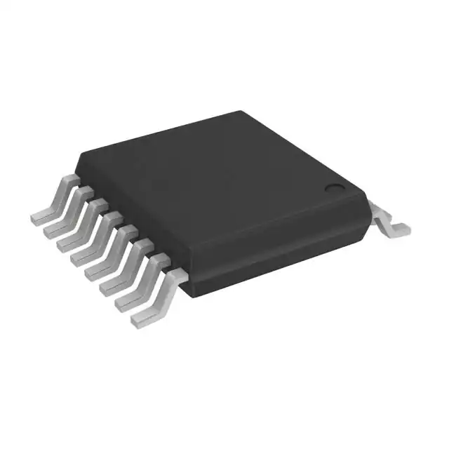
Ordering Information
Order
Number
Package
Number
Package Description
74VHC595M
M16A
16-Lead Small Outline Integrated Circuit (SOIC), JEDEC MS-012, 0.150" Narrow
74VHC595SJ
M16D
16-Lead Small Outline Package (SOP), EIAJ TYPE II, 5.3mm Wide
74VHC595MTC
MTC16
16-Lead Thin Shrink Small Outline Package (TSSOP), JEDEC MO-153, 4.4mm Wide
Surface mount packages are also available on Tape and Reel. Specify by appending the suffix letter “X” to the
ordering number.
©1993 Fairchild Semiconductor Corporation
74VHC595 Rev. 1.2
www.fairchildsemi.com
74VHC595 8-Bit Shift Register with Output Latches
May 2007
�74VHC595 8-Bit Shift Register with Output Latches
Connection Diagram
Logic Symbol
IEEE/IEC
Pin Description
Pin Names
Description
SER
Serial Data Input
SCK
Shift Register Clock Input
(Active rising edge)
RCK
Storage Register Clock Input
(Active rising edge)
SCLR
Reset Input
G
3-STATE Output Enable Input
(Active LOW)
QA – QH
Parallel Data Outputs
Q’H
Serial Data Output
Truth Table
Inputs
SER
RCK
SCK
SCLR
G
X
X
X
X
H
QA thru QH 3-STATE
X
X
X
X
L
QA thru QH outputs enabled
X
X
X
L
L
Shift Register cleared: Q′H = 0
L
X
↑
H
L
Shift Register clocked: QN = Qn-1, Q0 = SER = L
H
X
↑
H
L
Shift Register clocked: QN = Qn-1, Q0 = SER = H
X
↑
X
H
L
Contents of Shift Register transferred to output latches
©1993 Fairchild Semiconductor Corporation
74VHC595 Rev. 1.2
Function
www.fairchildsemi.com
2
�74VHC595 8-Bit Shift Register with Output Latches
Timing Diagram
©1993 Fairchild Semiconductor Corporation
74VHC595 Rev. 1.2
www.fairchildsemi.com
3
�74VHC595 8-Bit Shift Register with Output Latches
Logic Diagram (positive logic)
©1993 Fairchild Semiconductor Corporation
74VHC595 Rev. 1.2
www.fairchildsemi.com
4
�Symbol
Parameter
Rating
VCC
Supply Voltage
–0.5V to +7.0V
VIN
DC Input Voltage
–0.5V to +7.0V
VOUT
DC Output Voltage
–0.5V to VCC + 0.5V
IIK
Input Diode Current
–20mA
IOK
Output Diode Current
±20mA
IOUT
DC Output Current
±25mA
ICC
DC VCC / GND Current
TSTG
TL
±75mA
Storage Temperature
–65°C to +150°C
Lead Temperature (Soldering, 10 seconds)
260°C
Recommended Operating Conditions(1)
The Recommended Operating Conditions table defines the conditions for actual device operation. Recommended
operating conditions are specified to ensure optimal performance to the datasheet specifications. Fairchild does not
recommend exceeding them or designing to absolute maximum ratings.
Symbol
Parameter
VCC
Supply Voltage
VIN
Input Voltage
VOUT
Output Voltage
TOPR
Operating Temperature
t r, t f
Input Rise and Fall Time
Rating
2.0V to +5.5V
0V to +5.5V
0V to VCC
–40°C to +85°C
VCC = 3.3V ±0.3V
0 ∼ 100ns/V
VCC = 5.0V ±0.5V
0 ∼ 20ns/V
Note:
1. Unused inputs must be held HIGH or LOW. They may not float.
©1993 Fairchild Semiconductor Corporation
74VHC595 Rev. 1.2
www.fairchildsemi.com
5
74VHC595 8-Bit Shift Register with Output Latches
Absolute Maximum Ratings
Stresses exceeding the absolute maximum ratings may damage the device. The device may not function or be
operable above the recommended operating conditions and stressing the parts to these levels is not recommended.
In addition, extended exposure to stresses above the recommended operating conditions may affect device reliability.
The absolute maximum ratings are stress ratings only.
�TA = –40°C to
+85°C
TA = 25°C
Symbol Parameter
VCC (V) Conditions
VIH
HIGH Level Input
Voltage
VIL
LOW Level Input
Voltage
VOH
HIGH Level Output
Voltage
Min.
2.0
1.50
3.0 – 5.5
0.7 x VCC
3.0
LOW Level Output
Voltage
IOH = –50µA
2.0
1.9
2.9
3.0
2.9
4.4
4.5
4.4
2.58
2.48
IOH = –8mA
3.94
3.80
VIN = VIH
or VIL
IOL = 50µA
4.5
3-STATE Output
Off-State Current
IIN
Input Leakage
Current
ICC
Quiescent Supply
Current
V
0.0
0.1
0.1
0.0
0.1
0.1
0.0
IOL = 4mA
IOL = 8mA
V
0.3 x VCC
1.9
IOH = –4mA
3.0
V
0.50
4.5
2.0
Units
0.7 x VCC
3.0
3.0
Max.
0.3 x VCC
VIN = VIH
or VIL
4.5
IOZ
Min.
0.50
3.0 – 5.5
2.0
Max.
1.50
2.0
4.5
VOL
Typ.
0.1
0.1
0.36
0.44
V
0.36
0.44
VIN = VCC or GND,
VOUT = VCC or GND,
VING = VIH or VIL
±0.25
±2.5
µA
0 – 5.5
VIN = 5.5V or GND
±0.1
±1.0
µA
5.5
VIN = VCC or GND
4.0
40.0
µA
5.5
Noise Characteristics
TA = 25°C
Symbol
Parameter
VCC (V)
Conditions
Typ.
Limits
Units
Quiet Output Maximum
Dynamic VOL
5.0
CL = 50pF
0.9
1.2
V
VOLV(2)
Quiet Output Minimum
Dynamic VOL
5.0
CL = 50pF
–0.9
–1.2
V
VIHD(2)
Minimum HIGH Level
Dynamic Input Voltage
5.0
CL = 50pF
3.5
V
VILD(2)
Maximum LOW Level
Dynamic Input Voltage
5.0
CL = 50pF
1.5
V
VOLP
(2)
Note:
2. Parameter guaranteed by design.
©1993 Fairchild Semiconductor Corporation
74VHC595 Rev. 1.2
www.fairchildsemi.com
6
74VHC595 8-Bit Shift Register with Output Latches
DC Electrical Characteristics
�TA = –40°C
to +85°C
TA = +25°C
Symbol
Parameter
VCC (V)
Typ.
Max.
Min.
Max.
Units
tPLH, tPHL
Propagation Delay Time,
RCK to QA–QH
3.3 ± 0.3
CL = 15pF
7.7
11.9
1.0
13.5
ns
CL = 50pF
10.2
15.4
1.0
17.0
5.0 ± 0.5
CL = 15pF
5.4
7.4
1.0
8.5
CL = 50pF
6.9
9.4
1.0
10.5
3.3 ± 0.3
CL = 15pF
8.8
13.0
1.0
15.0
CL = 50pF
11.3
16.5
1.0
18.5
5.0 ± 0.5
CL = 15pF
6.2
8.2
1.0
9.4
CL = 50pF
7.7
10.2
1.0
11.4
3.3 ± 0.3
CL = 15pF
8.4
12.8
1.0
13.7
CL = 50pF
10.9
16.3
1.0
17.2
5.0 ± 0.5
CL = 15pF
5.9
8.0
1.0
9.1
CL = 50pF
7.4
10.0
1.0
11.1
CL = 15pF
7.5
11.5
1.0
13.5
CL = 50pF
9.0
15.0
1.0
17.0
CL = 15pF
4.8
8.6
1.0
10.0
tPLH, tPHL
tPHL
tPZL, tPZH
Propagation Delay Time,
SCK–Q'H
Propagation Delay Time,
SCLR –Q'H
Output Enable Time,
G to QA–QH
3.3 ± 0.3
Conditions
RL = 1kΩ
5.0 ± 0.5
tPLZ, tPHZ
fMAX
tOSLH, tOSHL
Output Disable Time,
G to QA–QH
Maximum Clock
Frequency
Output to Output Skew
3.3 ± 0.3
RL = 1kΩ
Min.
CL = 50pF
8.3
10.6
1.0
12.0
CL = 50pF
12.1
15.7
1.0
16.2
7.6
10.3
1.0
11.0
5.0 ± 0.5
CL = 50pF
3.3 ± 0.3
CL = 15pF
CL = 50pF
55
130
50
5.0 ± 0.5
CL = 15pF
135
185
115
CL = 50pF
95
155
3.3 ± 0.3
80
150
CL = 50pF
(3)
CL = 50pF
5.0 ± 0.5
70
ns
ns
ns
ns
ns
ns
ns
ns
MHz
MHz
85
1.5
1.5
1.0
1.0
10
10
ns
Input Capacitance
VCC = Open
5.0
COUT
Output Capacitance
VCC = 5.0V
6.0
pF
CPD
Power Dissipation
Capacitance
(4)
87
pF
CIN
pF
Notes:
3. Parameter guaranteed by design. tOSLH = | tPLH max – tPLH min|; tOSHL = | tPHL max – tPHL min|
4. CPD is defined as the value of the internal equivalent capacitance which is calculated from the operating
current consumption without load. Average operating current can be obtained by the equation:
ICC (Opr.) = CPD • VCC • fIN + ICC
©1993 Fairchild Semiconductor Corporation
74VHC595 Rev. 1.2
www.fairchildsemi.com
7
74VHC595 8-Bit Shift Register with Output Latches
AC Electrical Characteristics
�TA = 25°C
Symbol
tS
tS
tS
tH
tH
tH
tW(L)
Parameter
Minimum Setup Time (SER–SCK)
Minimum Setup Time (SCK–RCK)
Minimum Setup Time (SCLR–RCK)
Minimum Hold Time (SER–SCK)
Minimum Hold Time (SCK–RCK)
Minimum Hold Time (SCLR–RCK)
Minimum Pulse Width (SCLR)
tW(L), tW(H) Minimum Pulse Width (SCK)
tW(L), tW(H) Minimum Pulse Width (RCK)
trem
Minimum Removal Time (SCLR–SCK)
©1993 Fairchild Semiconductor Corporation
74VHC595 Rev. 1.2
VCC (V)
Typ.
TA = –40°C
to +85°C
Guaranteed Minimum Units
3.3 ± 0.3
3.5
3.5
5.0 ± 0.5
3.0
3.0
3.3 ± 0.3
8.0
8.5
5.0 ± 0.5
5.0
5.0
3.3 ± 0.3
8.0
9.0
5.0 ± 0.5
5.0
5.0
3.3 ± 0.3
1.5
1.5
5.0 ± 0.5
2.0
2.0
3.3 ± 0.3
0.0
0.0
5.0 ± 0.5
0.0
0.0
3.3 ± 0.3
0.0
0.0
5.0 ± 0.5
0.0
0.0
3.3 ± 0.3
5.0
5.0
5.0 ± 0.5
5.0
5.0
3.3 ± 0.3
5.0
5.0
5.0 ± 0.5
5.0
5.0
3.3 ± 0.3
5.0
5.0
5.0 ± 0.5
5.0
5.0
3.3 ± 0.3
3.0
3.0
5.0 ± 0.5
2.5
2.5
ns
ns
ns
ns
ns
ns
ns
ns
ns
ns
www.fairchildsemi.com
8
74VHC595 8-Bit Shift Register with Output Latches
AC Operating Requirements
�74VHC595 8-Bit Shift Register with Output Latches
Physical Dimensions
Dimensions are in millimeters unless otherwise noted.
Figure 1. 16-Lead Small Outline Integrated Circuit (SOIC), JEDEC MS-012, 0.150" Narrow
Package Number M16A
©1993 Fairchild Semiconductor Corporation
74VHC595 Rev. 1.2
www.fairchildsemi.com
9
�74VHC595 8-Bit Shift Register with Output Latches
Physical Dimensions (Continued)
Dimensions are in millimeters unless otherwise noted.
Figure 2. 16-Lead Small Outline Package (SOP), EIAJ TYPE II, 5.3mm Wide
Package Number M16D
©1993 Fairchild Semiconductor Corporation
74VHC595 Rev. 1.2
www.fairchildsemi.com
10
�5.00±0.10
4.55
5.90
4.45 7.35
0.65
4.4±0.1
1.45
5.00
0.11
12°
MTC16rev4
Figure 3. 16-Lead Thin Shrink Small Outline Package (TSSOP), JEDEC MO-153, 4.4mm Wide
Package Number MTC16
©1993 Fairchild Semiconductor Corporation
74VHC595 Rev. 1.2
www.fairchildsemi.com
11
74VHC595 8-Bit Shift Register with Output Latches
Physical Dimensions (Continued)
Dimensions are in millimeters unless otherwise noted.
�®
ACEx
Across the board. Around the world.™
ActiveArray™
Bottomless™
Build it Now™
CoolFET™
CorePLUS™
CROSSVOLT™
CTL™
Current Transfer Logic™
DOME™
2
E CMOS™
®
EcoSPARK
EnSigna™
FACT Quiet Series™
®
FACT
®
FAST
FASTr™
FPS™
®
FRFET
GlobalOptoisolator™
GTO™
HiSeC™
i-Lo™
ImpliedDisconnect™
IntelliMAX™
ISOPLANAR™
MICROCOUPLER™
MicroPak™
MICROWIRE™
Motion-SPM™
MSX™
MSXPro™
OCX™
OCXPro™
®
OPTOLOGIC
®
OPTOPLANAR
PACMAN™
PDP-SPM™
POP™
®
Power220
®
Power247
PowerEdge™
PowerSaver™
Power-SPM™
®
PowerTrench
Programmable Active Droop™
®
QFET
QS™
QT Optoelectronics™
Quiet Series™
RapidConfigure™
RapidConnect™
ScalarPump™
SMART START™
®
SPM
STEALTH™
SuperFET™
SuperSOT™-3
SuperSOT™-6
SuperSOT™-8
SyncFET™
TCM™
®
The Power Franchise
TinyBuck™
®
TinyLogic
TINYOPTO™
TinyPower™
TinyWire™
TruTranslation™
µSerDes™
®
UHC
UniFET™
VCX™
Wire™
™
TinyBoost™
DISCLAIMER
FAIRCHILD SEMICONDUCTOR RESERVES THE RIGHT TO MAKE CHANGES WITHOUT FURTHER NOTICE TO ANY PRODUCTS
HEREIN TO IMPROVE RELIABILITY, FUNCTION, OR DESIGN. FAIRCHILD DOES NOT ASSUME ANY LIABILITY ARISING OUT OF THE
APPLICATION OR USE OF ANY PRODUCT OR CIRCUIT DESCRIBED HEREIN; NEITHER DOES IT CONVEY ANY LICENSE UNDER ITS
PATENT RIGHTS, NOR THE RIGHTS OF OTHERS. THESE SPECIFICATIONS DO NOT EXPAND THE TERMS OF FAIRCHILD’S
WORLDWIDE TERMS AND CONDITIONS, SPECIFICALLY THE WARRANTY THEREIN, WHICH COVERS THESE PRODUCTS.
LIFE SUPPORT POLICY
FAIRCHILD’S PRODUCTS ARE NOT AUTHORIZED FOR USE AS CRITICAL COMPONENTS IN LIFE SUPPORT DEVICES OR
SYSTEMS WITHOUT THE EXPRESS WRITTEN APPROVAL OF FAIRCHILD SEMICONDUCTOR CORPORATION.
As used herein:
1. Life support devices or systems are devices or systems
which, (a) are intended for surgical implant into the body or
(b) support or sustain life, and (c) whose failure to perform
when properly used in accordance with instructions for use
provided in the labeling, can be reasonably expected to
result in a significant injury of the user.
2. A critical component in any component of a life support,
device, or system whose failure to perform can be
reasonably expected to cause the failure of the life support
device or system, or to affect its safety or effectiveness.
PRODUCT STATUS DEFINITIONS
Definition of Terms
Datasheet Identification
Product Status
Definition
Advance Information
Formative or In Design
This datasheet contains the design specifications for product
development. Specifications may change in any manner without notice.
Preliminary
First Production
This datasheet contains preliminary data; supplementary data will be
published at a later date. Fairchild Semiconductor reserves the right to
make changes at any time without notice to improve design.
No Identification Needed
Full Production
This datasheet contains final specifications. Fairchild Semiconductor
reserves the right to make changes at any time without notice to improve
design.
Obsolete
Not In Production
This datasheet contains specifications on a product that has been
discontinued by Fairchild Semiconductor. The datasheet is printed for
reference information only.
Rev. I27
©1993 Fairchild Semiconductor Corporation
74VHC595 Rev. 1.2
www.fairchildsemi.com
12
74VHC595 8-Bit Shift Register with Output Latches
TRADEMARKS
The following are registered and unregistered trademarks Fairchild Semiconductor owns or is authorized to use and is not intended to be an
exhaustive list of all such trademarks.
�ON Semiconductor and
are trademarks of Semiconductor Components Industries, LLC dba ON Semiconductor or its subsidiaries in the United States and/or other countries.
ON Semiconductor owns the rights to a number of patents, trademarks, copyrights, trade secrets, and other intellectual property. A listing of ON Semiconductor’s product/patent
coverage may be accessed at www.onsemi.com/site/pdf/Patent−Marking.pdf. ON Semiconductor reserves the right to make changes without further notice to any products herein.
ON Semiconductor makes no warranty, representation or guarantee regarding the suitability of its products for any particular purpose, nor does ON Semiconductor assume any liability
arising out of the application or use of any product or circuit, and specifically disclaims any and all liability, including without limitation special, consequential or incidental damages.
Buyer is responsible for its products and applications using ON Semiconductor products, including compliance with all laws, regulations and safety requirements or standards,
regardless of any support or applications information provided by ON Semiconductor. “Typical” parameters which may be provided in ON Semiconductor data sheets and/or
specifications can and do vary in different applications and actual performance may vary over time. All operating parameters, including “Typicals” must be validated for each customer
application by customer’s technical experts. ON Semiconductor does not convey any license under its patent rights nor the rights of others. ON Semiconductor products are not
designed, intended, or authorized for use as a critical component in life support systems or any FDA Class 3 medical devices or medical devices with a same or similar classification
in a foreign jurisdiction or any devices intended for implantation in the human body. Should Buyer purchase or use ON Semiconductor products for any such unintended or unauthorized
application, Buyer shall indemnify and hold ON Semiconductor and its officers, employees, subsidiaries, affiliates, and distributors harmless against all claims, costs, damages, and
expenses, and reasonable attorney fees arising out of, directly or indirectly, any claim of personal injury or death associated with such unintended or unauthorized use, even if such
claim alleges that ON Semiconductor was negligent regarding the design or manufacture of the part. ON Semiconductor is an Equal Opportunity/Affirmative Action Employer. This
literature is subject to all applicable copyright laws and is not for resale in any manner.
PUBLICATION ORDERING INFORMATION
LITERATURE FULFILLMENT:
Literature Distribution Center for ON Semiconductor
19521 E. 32nd Pkwy, Aurora, Colorado 80011 USA
Phone: 303−675−2175 or 800−344−3860 Toll Free USA/Canada
Fax: 303−675−2176 or 800−344−3867 Toll Free USA/Canada
Email: orderlit@onsemi.com
© Semiconductor Components Industries, LLC
N. American Technical Support: 800−282−9855 Toll Free
USA/Canada
Europe, Middle East and Africa Technical Support:
Phone: 421 33 790 2910
Japan Customer Focus Center
Phone: 81−3−5817−1050
www.onsemi.com
1
ON Semiconductor Website: www.onsemi.com
Order Literature: http://www.onsemi.com/orderlit
For additional information, please contact your local
Sales Representative
www.onsemi.com
�