80SQ045N
Preferred Device
Axial Lead Rectifier
These devices employ the Schottky Barrier principle in a large area
metal−to−silicon power diode. State−of−the−art geometry features
epitaxial construction with oxide passivation and metal overlap
contact. Ideally suited for use as rectifiers in low−voltage,
high−frequency inverters, free wheeling diodes, and polarity
protection diodes.
SCHOTTKY BARRIER
RECTIFIER
8.0 AMPERES
Features
•
•
•
•
•
•
•
•
http://onsemi.com
High Current Capability
Low Stored Charge, Majority Carrier Conduction
Low Power Loss/High Efficiency
Highly Stable Oxide Passivated Junction
Guard−Ring for Stress Protection
Low Forward Voltage
High Surge Capacity
These are Pb−Free Devices*
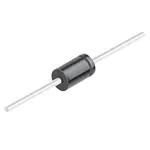
AXIAL LEAD
CASE 267−05
(DO−201AD)
STYLE 1
Mechanical Characteristics:
• Case: Epoxy, Molded
• Weight: 1.1 Gram (Approximately)
• Finish: All External Surfaces Corrosion Resistant and Terminal
Leads are Readily Solderable
• Lead and Mounting Surface Temperature for Soldering Purposes:
•
•
MARKING DIAGRAM
220°C Max. for 10 Seconds, 1/16″ from Case
Polarity: Cathode indicated by Polarity Band
ESD Protection: Human Body Model > 4000 V (Class 3)
Machine Model > 400 V (Class C)
80SQ
045N
YYWW G
G
MAXIMUM RATINGS
Rating
Symbol
Max
Unit
VRRM
VRWM
VR
45
V
IO
8.0
A
Non−Repetitive Peak Surge Current
(Surge Applied at Rated Load Conditions
Halfwave, Single Phase, 60 Hz)
IFSM
140
A
Operating and Storage Junction Temperature Range (Reverse Voltage Applied)
TJ, Tstg
−65 to +125
°C
dv/dt
10
V/ns
Peak Repetitive Reverse Voltage
Working Peak Reverse Voltage
DC Blocking Voltage
Average Rectified Forward Current TL = 75°C
(PsiJL = 12°C/W, P.C. Board Mounting, Note 2)
Voltage Rate of Change (Rated VR)
*For additional information on our Pb−Free strategy and soldering details, please
download the ON Semiconductor Soldering and Mounting Techniques
Reference Manual, SOLDERRM/D.
May, 2006 − Rev. 3
ORDERING INFORMATION
Package
Shipping †
80SQ045N
Axial Lead*
500 Units/Box
80SQ045NG
Axial Lead*
500 Units/Box
80SQ045NRL
Axial Lead*
1500/Tape & Reel
80SQ045NRLG
Axial Lead*
1500/Tape & Reel
Device
Stresses exceeding Maximum Ratings may damage the device. Maximum
Ratings are stress ratings only. Functional operation above the Recommended
Operating Conditions is not implied. Extended exposure to stresses above the
Recommended Operating Conditions may affect device reliability.
© Semiconductor Components Industries, LLC, 2006
YY
= Year
WW = Work Week
G
= Pb−Free Package
(Note: Microdot may be in either location)
1
†For information on tape and reel specifications,
including part orientation and tape sizes, please
refer to our Tape and Reel Packaging Specifications
Brochure, BRD8011/D.
*This package is inherently Pb−Free.
Preferred devices are recommended choices for future use
and best overall value.
Publication Order Number:
80SQ045N/D
�80SQ045N
THERMAL CHARACTERISTICS
Characteristic
Symbol
0.9 in x 0.9 in
Copper Pad Size
6.75 in x 6.75 in
Copper Pad Size
Thermal Resistance, Junction−to−Lead
(See Note 2 − Mounting Data)
Thermal Resistance, Junction−to−Ambient (See Note 2 − Mounting Data)
RqJL
RqJA
13
50
12
40
°C/W
Symbol
Max
Unit
Unit
ELECTRICAL CHARACTERISTICS (TL = 25°C unless otherwise noted)
Characteristic
Maximum Instantaneous Forward Voltage (Note 1)
(iF = 8.0 A, TL = 25°C)
vF
Maximum Instantaneous Reverse Current @ Rated dc Voltage (Note 1)
TL = 25°C
TL = 100°C
iR
V
0.55
mA
1.0
50
1. Pulse Test: Pulse Width = 300 ms, Duty Cycle = 2.0%.
30
IF, INSTANTANEOUS FORWARD
CURRENT (AMPS)
IF, INSTANTANEOUS FORWARD
CURRENT (AMPS)
30
10
100°C
1
0.1
75°C
125°C
25°C
0.1
0.2
0.3
0.4
0.5
0.6
0.7
VF, INSTANTANEOUS VOLTAGE (VOLTS)
10
MBR845
1
0.1
0.8
100°C
25°C
0.1
IR, INSTANTANEOUS REVERSE CURRENT (AMPS)
Figure 1. Typical Forward Voltage
0.2
0.3
0.4
0.5
0.6
0.7
VF, INSTANTANEOUS VOLTAGE (VOLTS)
0.8
Figure 2. Maximum Forward Voltage
10,000
1E−01
C, CAPACITANCE (pF)
125°C
1E−02
100°C
75°C
1E−03
1E−04
25°C
1E−05
1E−06
75°C
125°C
f = 1 MHz
TJ = 25°C
1000
100
0
5
10 15 20
25 30 35 40
VR, REVERSE VOLTAGE (VOLTS)
45
50
0.1
Figure 3. Typical Reverse Current
1
10
VR, REVERSE VOLTAGE (VOLTS)
Figure 4. Typical Capacitance
http://onsemi.com
2
100
�75
9
70
8
IF, AVERAGE FORWARD
CURRENT (AMPS)
COPPER AREA (sq in)
80SQ045N
65
60
55
50
See Note 2
45
40
dc
RqJL = 12°C/W
7
6
SQUARE
WAVE
5
4
3
2
1
35
0
30
0
2
4
6
8
0
10
20
40
60
80
100
120
RqJA (°C/W)
TL, LEAD TEMPERATURE (°C)
Figure 5. RqJA versus Copper Area
Figure 6. Current Derating − Lead
140
4.5
NOTE 2 — MOUNTING DATA
PFO, AVERAGE POWER
DISSIPATION (WATTS)
4
3.5
Mounting Method
SQUARE
WAVE
3
P.C. Board with 6.75 sq. in.
copper surface.
TJ = 125°C
ÉÉ
ÉÉ
ÉÉ
ÉÉ
ÉÉ
ÉÉ
ÉÉ
ÉÉ
2.5
dc
2
1.5
1
0.5
0
0
2
4
6
10
8
IO, AVERAGE FORWARD CURRENT (AMPS)
r(t), NORMALIZED EFFECTIVE TRANSIENT
THERMAL RESISTANCE
Figure 7. Forward Power Dissipation
1
L = 3/8,
Board Ground Plane
D = 0.5
0.2
0.1
0.1
0.05
P(pk)
0.01
Copper Area = 0.271 sq. in.
0.01
0.001
0.0001
t1
RqJA = 61.8 °C/W
SINGLE PULSE
0.001
0.01
0.1
1.0
t, TIME (sec)
Figure 8. Thermal Response, Junction−to−Ambient
http://onsemi.com
3
t2
DUTY CYCLE, D = t1/t2
10
100
1000
�MECHANICAL CASE OUTLINE
PACKAGE DIMENSIONS
AXIAL LEAD
CASE 267−05
ISSUE G
DATE 06/06/2000
SCALE 1:1
K
D
NOTES:
1. DIMENSIONS AND TOLERANCING PER ANSI
Y14.5M, 1982.
2. CONTROLLING DIMENSION: INCH.
3. 267-04 OBSOLETE, NEW STANDARD 267-05.
A
1
2
B
K
STYLE 1:
PIN 1. CATHODE (POLARITY BAND)
2. ANODE
DOCUMENT NUMBER:
DESCRIPTION:
DIM
A
B
D
K
98ASB42170B
AXIAL LEAD
INCHES
MIN
MAX
0.287
0.374
0.189
0.209
0.047
0.051
1.000
---
MILLIMETERS
MIN
MAX
7.30
9.50
4.80
5.30
1.20
1.30
25.40
---
STYLE 2:
NO POLARITY
Electronic versions are uncontrolled except when accessed directly from the Document Repository.
Printed versions are uncontrolled except when stamped “CONTROLLED COPY” in red.
PAGE 1 OF 1
ON Semiconductor and
are trademarks of Semiconductor Components Industries, LLC dba ON Semiconductor or its subsidiaries in the United States and/or other countries.
ON Semiconductor reserves the right to make changes without further notice to any products herein. ON Semiconductor makes no warranty, representation or guarantee regarding
the suitability of its products for any particular purpose, nor does ON Semiconductor assume any liability arising out of the application or use of any product or circuit, and specifically
disclaims any and all liability, including without limitation special, consequential or incidental damages. ON Semiconductor does not convey any license under its patent rights nor the
rights of others.
© Semiconductor Components Industries, LLC, 2019
www.onsemi.com
�onsemi,
, and other names, marks, and brands are registered and/or common law trademarks of Semiconductor Components Industries, LLC dba “onsemi” or its affiliates
and/or subsidiaries in the United States and/or other countries. onsemi owns the rights to a number of patents, trademarks, copyrights, trade secrets, and other intellectual property.
A listing of onsemi’s product/patent coverage may be accessed at www.onsemi.com/site/pdf/Patent−Marking.pdf. onsemi reserves the right to make changes at any time to any
products or information herein, without notice. The information herein is provided “as−is” and onsemi makes no warranty, representation or guarantee regarding the accuracy of the
information, product features, availability, functionality, or suitability of its products for any particular purpose, nor does onsemi assume any liability arising out of the application or use
of any product or circuit, and specifically disclaims any and all liability, including without limitation special, consequential or incidental damages. Buyer is responsible for its products
and applications using onsemi products, including compliance with all laws, regulations and safety requirements or standards, regardless of any support or applications information
provided by onsemi. “Typical” parameters which may be provided in onsemi data sheets and/or specifications can and do vary in different applications and actual performance may
vary over time. All operating parameters, including “Typicals” must be validated for each customer application by customer’s technical experts. onsemi does not convey any license
under any of its intellectual property rights nor the rights of others. onsemi products are not designed, intended, or authorized for use as a critical component in life support systems
or any FDA Class 3 medical devices or medical devices with a same or similar classification in a foreign jurisdiction or any devices intended for implantation in the human body. Should
Buyer purchase or use onsemi products for any such unintended or unauthorized application, Buyer shall indemnify and hold onsemi and its officers, employees, subsidiaries, affiliates,
and distributors harmless against all claims, costs, damages, and expenses, and reasonable attorney fees arising out of, directly or indirectly, any claim of personal injury or death
associated with such unintended or unauthorized use, even if such claim alleges that onsemi was negligent regarding the design or manufacture of the part. onsemi is an Equal
Opportunity/Affirmative Action Employer. This literature is subject to all applicable copyright laws and is not for resale in any manner.
PUBLICATION ORDERING INFORMATION
LITERATURE FULFILLMENT:
Email Requests to: orderlit@onsemi.com
onsemi Website: www.onsemi.com
◊
TECHNICAL SUPPORT
North American Technical Support:
Voice Mail: 1 800−282−9855 Toll Free USA/Canada
Phone: 011 421 33 790 2910
Europe, Middle East and Africa Technical Support:
Phone: 00421 33 790 2910
For additional information, please contact your local Sales Representative
�