ON Semiconductor
Is Now
To learn more about onsemi™, please visit our website at
www.onsemi.com
onsemi and and other names, marks, and brands are registered and/or common law trademarks of Semiconductor Components Industries, LLC dba “onsemi” or its affiliates and/or
subsidiaries in the United States and/or other countries. onsemi owns the rights to a number of patents, trademarks, copyrights, trade secrets, and other intellectual property. A listing of onsemi
product/patent coverage may be accessed at www.onsemi.com/site/pdf/Patent-Marking.pdf. onsemi reserves the right to make changes at any time to any products or information herein, without
notice. The information herein is provided “as-is” and onsemi makes no warranty, representation or guarantee regarding the accuracy of the information, product features, availability, functionality,
or suitability of its products for any particular purpose, nor does onsemi assume any liability arising out of the application or use of any product or circuit, and specifically disclaims any and all
liability, including without limitation special, consequential or incidental damages. Buyer is responsible for its products and applications using onsemi products, including compliance with all laws,
regulations and safety requirements or standards, regardless of any support or applications information provided by onsemi. “Typical” parameters which may be provided in onsemi data sheets and/
or specifications can and do vary in different applications and actual performance may vary over time. All operating parameters, including “Typicals” must be validated for each customer application
by customer’s technical experts. onsemi does not convey any license under any of its intellectual property rights nor the rights of others. onsemi products are not designed, intended, or authorized
for use as a critical component in life support systems or any FDA Class 3 medical devices or medical devices with a same or similar classification in a foreign jurisdiction or any devices intended for
implantation in the human body. Should Buyer purchase or use onsemi products for any such unintended or unauthorized application, Buyer shall indemnify and hold onsemi and its officers, employees,
subsidiaries, affiliates, and distributors harmless against all claims, costs, damages, and expenses, and reasonable attorney fees arising out of, directly or indirectly, any claim of personal injury or death
associated with such unintended or unauthorized use, even if such claim alleges that onsemi was negligent regarding the design or manufacture of the part. onsemi is an Equal Opportunity/Affirmative
Action Employer. This literature is subject to all applicable copyright laws and is not for resale in any manner. Other names and brands may be claimed as the property of others.
�A5191HRT
HART Modem
Description
The A5191HRT is a single−chip, CMOS modem for use in highway
addressable remote transducer (HART) field instruments and masters.
The modem and a few external passive components provide all of the
functions needed to satisfy HART physical layer requirements
including modulation, demodulation, receive filtering, carrier detect,
and transmit−signal shaping.
The A5191HRT uses phase continuous frequency shift keying
(FSK) at 1200 bits per second. To conserve power the receive circuits
are disabled during transmit operations and vice versa. This provides
the half−duplex operation used in HART communications.
Features
•
•
•
•
•
•
•
•
•
•
•
•
Single−chip, Half−duplex 1200 Bits per Second FSK Modem
Bell 202 Shift Frequencies of 1200 Hz and 2200 Hz
3.0 V − 5.5 V Power Supply
Transmit−signal Wave Shaping
Receive Band−pass Filter
Low Power: Optimal for Intrinsically Safe Applications
Compatible with 3.3 V or 5 V Microcontroller
Internal Oscillator Requires 460.8 kHz Crystal or Ceramic Resonator
Meets HART Physical Layer Requirements
Industrial Temperature Range of −40°C to +85°C
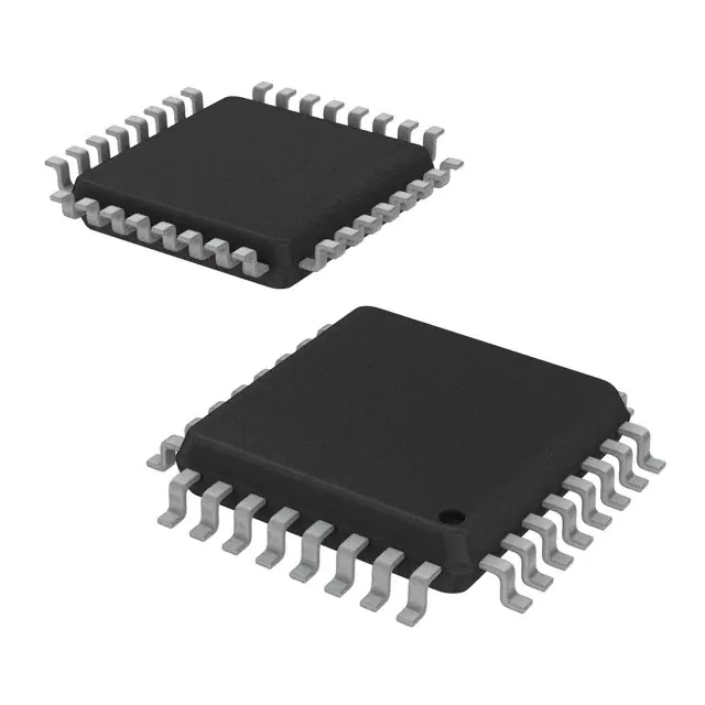
Available in 28−pin PLCC, 32−pin QFN and 32−pin LQFP Packages
These are Pb−Free Devices
www.onsemi.com
PLCC−28
P SUFFIX
CASE 776AA
QFN−32
N SUFFIX
CASE 488AM
LQFP−32
L SUFFIX
CASE 561AB
MARKING DIAGRAMS
(Top Views)
1 28
A5191HRTPG
AWLYYWW
A5191
HRTL
AWLYYWWG
Applications
• HART Multiplexers
• HART Modem Interfaces
• 4 − 20 mA Loop Powered Transmitters
32
1
1
A5191
HRTNG
AWLYYWW
G
A5191HRTxx = Specific Device Code
xx
= P (PLCC), L (LQFP) or N (QFN)
A
= Assembly Location
WL
= Wafer Lot
YY
= Year
WW
= Work Week
G or G = Pb−Free Package
ORDERING INFORMATION
See detailed ordering and shipping information in the package
dimensions section on page 14 of this data sheet.
© Semiconductor Components Industries, LLC, 2014
April, 2018 − Rev. 10
1
Publication Order Number:
A5191HRT/D
�A5191HRT
BLOCK DIAGRAM
VDD
VDDA
RxAFI
RxAF
RESET
RxA
Demodulator
Logic
Rx Comp
FSK_IN
Rx HP Filter
RxD
AREF
Carrier Detect
Counter
CD
CDREF
Carrier Comp
Numeric
Controlled
Oscillator
TxD
DEMODULATOR
TxA
Sine
Shaper
FSK_OUT
MODULATOR
RTS
Crystal
Oscillator
XOUT XIN
A5191HRT
BIAS
CBIAS
VSS
VSSA
Figure 1. Block Diagram A5191HRT
ELECTRICAL SPECIFICATIONS
Table 1. ABSOLUTE MAXIMUM RATINGS (Notes 1 and 2)
Parameter
Symbol
Min
Max
Units
TA
Ambient
−40
+85
°C
TS
Storage Temperature
−55
+150
°C
TJ
Junction Temperature
−40
+85
°C
Supply Voltage
−0.3
6.0
V
DC Input, Output
−0.3
VDD + 0.3
V
VDD
VIN, VOUT
Stresses exceeding those listed in the Maximum Ratings table may damage the device. If any of these limits are exceeded, device functionality
should not be assumed, damage may occur and reliability may be affected.
1. CMOS devices are damaged by high−energy electrostatic discharge. Devices must be stored in conductive foam or with all pins shunted.
Precautions should be taken to avoid application of voltages higher than the maximum rating. Stresses above absolute maximum ratings
may result in damage to the device.
2. Remove power before insertion or removal of this device.
www.onsemi.com
2
�A5191HRT
Table 2. DC CHARACTERISTICS (VDD = 3.0 V to 5.5 V, VSS = 0 V, TA = −40°C to +85°C)
Parameter
Symbol
VDD
VIL
Input Voltage, Low
3.0 – 5.5 V
VIH
Input Voltage, High
3.0 – 5.5 V
VOL
Output Voltage, Low (IOL = 0.67 mA)
3.0 – 5.5 V
VOH
Output Voltage, High (IOH = −0.67 mA)
3.0 – 5.5 V
CIN
Input Capacitance of:
Analog Input
RXA
Digital Input
Min
Typ
Max
Units
0.3 * VDD
V
0.7 * VDD
V
0.4
V
2.4
V
2.9
25
3.5
pF
pF
pF
IIL/IIH
Input Leakage Current
±500
nA
IOLL
Output Leakage Current
±10
mA
IDDA
Power Supply Current
(RBIAS = 500 kW, AREF = 1.235 V)
3.3 V
5.0 V
150
150
450
600
mA
mA
IDDD
Dynamic Digital Current
5.0 V
25
200
mA
AREF
Analog Reference
3.3 V
5.0 V
1.2
2.6
V
V
Carrier Detect Reference (AREF – 0.08 V)
3.3 V
5.0 V
CDREF
(Note 3)
CBIAS
330
300
1.235
2.5
Comparator Bias Current
(RBIAS = 500 kW, AREF = 1.235 V)
1.15
2.42
V
2.5
mA
3. The HART specification requires carrier detect (CD) to be active between 80 and 120 mVp−p. Setting CDREF at AREF − 0.08 VDC will set
the carrier detect to a nominal 100 mVp−p.
Table 3. AC CHARACTERISTICS (VDD = 3.0 V to 5.5 V, VSS = 0 V, TA = −40°C to +85°C) (Note 4)
Pin Name
RxA
RxAF
RxAFI
TxA
RxD
CD
Description
Min
Typ
Max
Units
Receive analog input
Leakage current
Frequency – mark (logic 1)
Frequency – space (logic 0)
1190
2180
1200
2200
±150
1210
2220
nA
Hz
Hz
Output of the high−pass filter
Slew rate
Gain bandwidth (GBW)
Voltage range
150
0.15
VDD – 0.15
V/ms
kHz
V
±500
nA
0.025
Carrier detect and receive filter input
Leakage current
Modulator output
Frequency – mark (logic 1)
Frequency – space (logic 0)
Amplitude (AREF 1.235 V)
Slew Rate − mark (logic 1)
Slew Rate − space (logic 0)
Loading (AREF = 1.235 V)
30
Receive digital output
Rise/fall time
20
Carrier detect output
Rise/fall time
20
1196.9
2194.3
500
1860
3300
Hz
Hz
mV
V/s
V/s
kW
ns
ns
Product parametric performance is indicated in the Electrical Characteristics for the listed test conditions, unless otherwise noted. Product
performance may not be indicated by the Electrical Characteristics if operated under different conditions.
4. The modular output frequencies are proportional to the input clock frequency (460.8 kHz).
www.onsemi.com
3
�A5191HRT
Table 4. MODEM CHARACTERISTICS (VDD = 3.0 V to 5.5 V, VSS = 0 V, TA = −40°C to +85°C)
Min
Parameter
Typ
Demodulator jitter
Conditions
1. Input frequencies at 1200 Hz ± 10 Hz, 2200 Hz ± 20 Hz
2. Clock frequency of 460.8 kHz ± 0.1%
3. Input (RxA) asymmetry, 0
Max
Units
12
% of 1 bit
Table 5. CERAMIC RESONATOR − External Clock Specifications (VDD = 3.0 V to 5.5 V, VSS = 0 V, TA = −40°C to +85°C)
Parameter
Min
Typ
Resonator
Tolerance
Frequency
Max
Units
1.0
%
kHz
465.4
60
kHz
%
V
460.8
External
Clock frequency
Duty cycle
Amplitude
456.2
40
460.8
50
VOH − VOL
TYPICAL APPLICATION
POWER
3.0 to 5.5 V
VDD
NCP301
VDDA
RxAFI
RxAF
RxA
RESET
VDDA
RxD
AREF
CD
A5191HRT
LM285
mC
HART IN
TxD
CDREF
RTS
TxA
XOUT
460.8 kHz
XIN
CBIAS
VSS
S
VSSA
4 – 20 mA
DAC OUT
Figure 2. Application Diagram A5191HRT
www.onsemi.com
4
HART &
4 – 20 mA OUT
�TEST4
TEST3
TEST2
TEST1
TEST12
CD
RxD
A5191HRT
4
3
2
1
28
27
26
TEST5
5
25
TEST11
RESET
6
24
TxD
TEST7
7
23
RTS
TEST8
8
22
VDD
TEST9
9
21
VSS
A5191HRT
12
13
14
15
16
17
18
RxAF
RxAFI
XOUT
RxA
AREF
19
VDDA
XIN
11
TEST10
20
CBIAS
10
CDREF
TxA
Figure 3. Pin Out A5191HRT in 28-pin PLCC
Table 6. PIN OUT SUMMARY 28−PIN PLCC
Pin No.
Signal Name
Type
Pin Description
1
TEST1
Input
Connect to VSS
2, 3, 4
TEST2, 3, 4
−
Do Not Connect
5
TEST5
Input
Connect to VSS
6
RESETB
Input
Reset all digital logic when low
7, 8, 9
TEST7, 8, 9
Input
Connect to VSS
10
TxA
Output
11
AREF
Input
Analog reference voltage
12
CDREF
Input
Carrier detect reference voltage
13
CBIAS
Output
14
TEST10
Input
15
VDDA
Power
Transmit Data Modulator output
Comparator bias current
Connect to VSS
Analog supply voltage
16
RxA
Input
17
RxAF
Output
Receive Data Modulator input
18
RxAFI
Input
19
XOUT
Output
20
XIN
Input
21
VSS
Ground
Ground
22
VDD
Power
Digital supply voltage
23
RTSB
Input
Request to send
24
TxD
Input
Input transmit date, transmitted HART data stream from microcontroller
25
TEST11
−
26
RxD
Output
Received demodulated HART data to microcontroller
27
CD
Output
Carrier detect output
28
TEST12
−
Analog receive filter output
Analog receive comparator input
Crystal oscillator output
Crystal oscillator input
Do Not Connect
Do Not Connect
www.onsemi.com
5
�TEST12
CD
RxD
26
25
TEST1
28
27
VDD
TEST2
29
TEST3
30
TEST4
32
RxD
25
31
TEST12
CD
26
TEST1
28
27
VDD
TEST2
29
TEST3
31
30
TEST4
32
A5191HRT
TEST5
1
24
TEST11
TEST5
1
24
RESET
2
23
TxD
RESET
2
23
TxD
TEST7
3
22
RTS
TEST7
3
22
RTS
21
VDD
TEST8
4
21
VDD
20
VSS
TEST9
5
20
VSS
TEST11
TEST8
4
TEST9
5
VSS
6
19
VSSA
VSS
6
19
VSSA
TxA
AREF
7
18
XIN
TxA
7
18
XIN
8
17
XOUT
AREF
8
17
XOUT
12
13
14
15
16
VDDA
RxA
RxAF
RxAFI
RxAFI
VSSA
16
RxAF
11
15
RxA
TEST10
14
VDDA
9
13
VSSA
10
12
TEST10
CBIAS
11
CBIAS
A5191HRT
CDREF
9
10
CDREF
A5191HRT
Figure 4. Pin Out A5191HRT in 32-pin QFN and LQFP (top view)
Table 7. PIN OUT SUMMARY 32−PIN QFN AND LQFP
Pin No.
Signal Name
Type
Pin Description
1
TEST5
Input
Connect to VSS
2
RESETB
Input
Reset all logic when low, connect to VDD for normal operation
3, 4, 5
TEST7, 8, 9
Input
Connect to VSS
6
VSS
Ground
Digital ground
7
TxA
Output
Transmit Data Modulator output
8
AREF
Input
Analog reference voltage
Carrier detect reference voltage
9
CDREF
Input
10
CBIAS
Output
11
TEST10
Input
12
VSSA
Ground
Analog ground
13
VDDA
Power
Analog supply voltage
14
RxA
Input
15
RxAF
Output
16
RxAFI
Input
17
XOUT
Output
18
XIN
Input
19
VSSA
Ground
Analog ground
20
VSS
Ground
Digital ground
21
VDD
Power
Digital supply voltage
22
RTSB
Input
Request to send
23
TxD
Input
Input transmit data, transmit HART data stream from microcontroller
24
TEST11
−
25
RxD
Output
Received demodulated HART data to microcontroller
26
CD
Output
Carrier detect output
27
TEST12
−
Do Not Connect
28
TEST1
Input
Connect to VSS
29
TEST2
−
Do Not Connect
30
VDD
Power
31, 32
TEST3, 4
−
EP
Exposed Pad
Power
Comparator bias current
Connect to VSS
Receive Data Modulator input
Analog receive filter output
Analog receive comparator input
Crystal oscillator output
Crystal oscillator input
Do Not Connect
Digital supply voltage
Do Not Connect
Connect to VSS (QFN only)
www.onsemi.com
6
�A5191HRT
Pin Descriptions
Table 8. PIN DESCRIPTIONS
Symbol
Pin Name
Description
AREF
Analog reference voltage
Receiver Reference Voltage. Normally 1.23 V is selected (in combination with
VDDA = 3.3 V). See Table 2.
CDREF
Carrier detect reference voltage
Carrier Detect Reference voltage. The value should be 85 mV below AREF to set
the carrier detection to a nominal of 100 mVp−p.
RESETB
Reset digital logic
When at logic low (VSS) this input holds all the digital logic in reset. During normal
operation RESETB should be at VDD. RESETB should be held low for a minimum
of 10 nS after VDD = 2.5 V as shown in Figure 14.
RTSB
Request to send
Active−low input selects the operation of the modulator. TxA is enabled when this
signal is low. This signal must be held high during power−up.
RxA
Analog receive input
Receive Data Demodulator Input. Accepts a HART 1200 / 2200 Hz FSK modulated waveform input.
RxAFI
Analog receive comparator input
Positive input of the carrier detect comparator and the receiver filter comparator.
TxD
Digital transmit input
Input to the modulator accepts digital data in NRZ form. When TxD is low, the
modulator output frequency is 2200 Hz. When TxD is high, the modulator output
frequency is 1200 Hz.
XIN
Oscillator input
Input to the internal oscillator must be connected to a parallel mode 460.8 kHz
ceramic resonator when using the internal oscillator or grounded when using an
external 460.8 kHz clock signal.
CBIAS
Comparator bias current
Connection to the external bias resistor. RBIAS should be selected such that
AREF / RBIAS = 2.5 mA ± 5 %
CD
Carrier detect output
Output goes high when a valid input is recognized on RxA. If the received signal
is greater than the threshold specified on CDREF for four cycles of the RxA signal, the valid input is recognized.
RxAF
Analog receive filter output
The output of the three pole high pass receive data filter
RxD
Digital receive output
Signal outputs the digital receive data. When the received signal (RxA) is
1200 Hz, RxD outputs logic high. When the received signal (RxA) is 2200 Hz,
RxD outputs logic low. The HART receive data stream is only active if Carrier
Detect (CD) is high.
TxA
Analog transmit output
Transmit Data Modulator Output. A trapezoidal shaped waveform with a frequency of 1200 Hz or 2200 Hz corresponding to a data value of 1 or 0 respectively applied to TxD. TxA is active when RTSB is low. TxA equals 0.5 V when
RTSB is high.
XOUT
Oscillator output
Output from the internal oscillator must be connected to an external 460.8 kHz
clock signal or to a parallel mode 460.8 kHz ceramic resonator when using the
internal oscillator.
TEST(12:1)
Factory test
Factory test pins; for normal operation, tie these signals as per Tables 6 and 7
VDD
Digital power
Power for the digital modem circuitry
VDDA
Analog supply voltage
Power for the analog modem circuitry
VSS
Ground
Digital ground (and Analog ground in the case of PLCC package)
VSSA
Analog ground
Analog ground
www.onsemi.com
7
�A5191HRT
Functional Description
The A5191HRT is a single-chip modem for use in
Highway Addressable Remote Transducer (HART) field
instruments and masters. The modem IC contains a transmit
data modulator with signal shaper, carrier detect circuitry, an
analog receiver, demodulator circuitry and a crystal
oscillator, as shown in the block diagram in Figure 1.
The modulator accepts digital data at its digital input TxD
and generates a sine shaped FSK modulated signal at the
analog output TxA. A digital “1” or mark is represented with
a frequency of 1200 Hz. A digital “0” or space is represented
with a frequency of 2200 Hz. The used bit rate is 1200 baud.
The demodulator receives the FSK signal at its analog
input, filters it with a band-pass filter and generates 2 digital
signals: RxD: Received Data and CD: Carrier Detect. At the
digital output RxD the original modulated signal is received.
CD outputs the Carrier Detect signal. It goes logic high if the
received signal is above 100 mVpp during 4 consecutive
carrier periods.
The oscillator provides the modem with a stable time base
using either a simple external resonator or an external clock
source.
The Numeric Controlled Oscillator NCO works in a phase
continuous mode preventing abrupt phase shifts when
switching between mark and space frequency. The control
signal Request To Send RTSB enables the NCO. When
RTSB is logic low the modulator is active and A5191HRT
is in transmit mode. When RTSB is logic high the modulator
is disabled and A5191HRT is in receive mode.
The digital outputs of the NCO are shaped in the Wave
Shaper block to a trapezoidal signal. This circuit controls the
rising and falling edge to be inside the standard HART
waveshape limits. Figure 7 shows the transmit-signal forms
captured at TxA for mark and space frequency. The slew
rates are SRm = 1860 V/s at the mark frequency and SRs =
3300 V/s at the space frequency. For AREF = 1.235 V, TxA
will have a voltage swing from approximately 0.25 to 0.75
VDC.
VTxA
“1” = Mark; fm =1.2 kHz
0.5 V
0.5 V
SRm = 1860 V/s
Detailed Description
0
Modulator
1
VTxA
The modulator accepts digital data in NRZ form at the
TxD input and generates the FSK modulated signal at the
TxA output.
t (ms)
2
“0” = Space; fs =2.2 kHz
0.5 V
0.5 V
t (ms)
SRs = 3300 V/s
TxD
Numeric
Controlled
Oscillator
RTS
TxA
Sine
Shaper
0
FSK_OUT
2
Figure 7. Modulator shaped output signal for Mark
and Space frequency at TxA pin.
MODULATOR
Figure 5. Modulator Block Diagram
Demodulator
A logic “1” or mark is represented by a frequency fm =
1200 Hz. A logic “0”or space is represented by a frequency
fs = 2200 Hz.
“1” = Mark
1.2 kHz
1
The demodulator accepts a FSK signal at the RxA input
and reconstructs the original modulated signal at the RxD
output. Figure 8 illustrates the demodulation process.
“0” = Space
2.2 kHz
FSK_IN
RxD
LSB
IDLE (mark)
t
MSB
Start
D0
D1
D2
“0”
“1”
“0”
“1”
tBIT
IDLE (mark)
D3
D4
D5
D6
D7
Par
“0”
“0”
“1”
“0”
“1”
“0”
8 data bits
Stop
t BIT
Figure 8. Modulation Timing
tBIT = 833 ms
This HART bit stream follows a standard 11-bit UART
frame with 1 startbit, 8 databits, 1 paritybit (odd) and 1
stopbit. The communication speed is 1200 baud.
tBIT = 454 m s
Figure 6. Modulation Timing
www.onsemi.com
8
�A5191HRT
Receive Filter and Comparator
output pin CD high if RTSB is high and four consecutive
pulses out of the comparator have arrived. CD stays high as
long as RTSB is high and the next comparator pulse is
received in less than 2.5 ms. Once CD goes inactive, it takes
four consecutive pulses out of the comparator to assert CD
again. Four consecutive pulses amount to 3.33 ms when the
received signal is 1200 Hz and to 1.82 ms when the received
signal is 2200 HZ.
The received FSK signal first is filtered using a band-pass
filter build around the low noise receiver operational
amplifier “Rx HP filter”. This filter blocks interferences
outside the HART signal band.
R6
R5
RxAF
RxAFI
Miscellaneous Analog Circuitry
HART IN
15 MW
RxA
Rx Comp
C3
C2
R4
Rx HP Filter
DEMODULATOR
R3
AREF
C1
Voltage References
The A5191HRT requires two voltage references, AREF
and CDREF. AREF sets the DC operating point of the
internal operational amplifiers and is the reference for the
Rx comparator. If A5191HRT operates at VDD = 3.3 V the
ON Semiconductor LM285D 1.235 V reference is
recommended.
The level at which CD (Carrier Detect) becomes active is
determined by the DC voltage difference (CDREF - AREF).
Selecting a voltage difference of 80 mV will set the carrier
detect to a nominal 100 mVp-p.
R1
R2
1.235 VDC
Figure 9. Demodulator Receive Filter and Signal
Comparator
The filter output is fed into the Rx comparator. The
threshold value equals the analog ground making the
comparator to toggle on every zero crossing of the filtered
FSK signal. The maximum demodulator jitter is 12 % of one
bit given the input frequencies are within the HART
specifications, a clock frequency of 460.8 kHz (±1.0 %) and
zero input (RxA) asymmetry.
Bias Current Resistor
The A5191HRT requires a bias current resistor RBIAS to
be connected between CBIAS and VSS. The bias current
controls the operating parameters of the internal operational
amplifiers and comparators and should be set to 2.5 mA.
Carrier Detect Circuitry
Low HART input signal levels increases the risk for the
generation of bit errors. Therefore the minimum signal
amplitude is set to 80 − 120 mVpp. If the received signal is
below this level the demodulator is disabled.
This level detection is done in the Carrier Detector. The
output of the demodulator is qualified with the carrier detect
signal (CD), therefore, only RxA signals large enough to be
detected (100 mVp-p typically) by the carrier detect circuit
produce received serial data at RxD.
BIAS
2.5 mA
C4
AREF
OPA
FILTERED
HART IN
RxAFI
CBIAS
RBIAS
Demodulator
Logic
15 MW
RxD
Figure 11. Bias Circuit
Rx Comp
AREF
CD
Carrier Detect
Counter
DEMODULATOR
The value of the bias current resistor is determined by the
reference voltage AREF and the following formula:
1.235 VDC
CDREF
R BIAS + AREF
2.5 mA
VAREF – 80 mV
Carrier Comp
The recommended bias current resistor is 500 KW when
AREF is equal to 1.235 V.
Figure 10. Demodulator Carrier and Signal
Comparator
Oscillator
The carrier detect comparator shown in Figure 10
generates logic low output if the RxAFI voltage is below
CDREF. The comparator output is fed into a carrier detect
block. The carrier detect block drives the carrier detect
The A5191HRT requires a 460.8 kHz clock signal. This
can be provided by an external clock or a resonator
connected to the A5191HRT internal oscillator.
www.onsemi.com
9
�A5191HRT
Internal Oscillator Option
The oscillator cell will function with either a 460.8 kHz
crystal or ceramic resonator. A parallel resonant ceramic
resonator can be connected between XIN and XOUT.
Figure 12 illustrates the crystal option for clock generation
using a 460.8 kHz (±1 % tolerance) parallel resonant crystal
and two tuning capacitors Cx. The actual values of the
capacitors may depend on the recommendations of the
manufacturer of the resonator. Typically, capacitors in the
range of 100 pF to 470 pF are used.
Crystal
Oscillator
XOUT
XIN
460.8 kHz
Figure 13. Oscillator with External Clock
Power On Reset
During start-up the RESETB pin should be kept low until
the voltage level on VDD is above the minimum level VDDH
= 2.5 V to guarantee correct operation of the digital circuitry.
As illustrated in Figure 14 RESETB should be kept low for
at least tPOR = 10 ns after this threshold level is reached.
Crystal
Oscillator
XOUT
460.8 kHz
XIN
VDD
CX
CX
VDDH = 2.5 V
t
Figure 12. Crystal Oscillator
RESET pin
External Clock Option
It may be desirable to use an external 460.8 kHz clock as
shown in Figure 13 rather than the internal oscillator. In
addition, the A5191HRT consumes less current when an
external clock is used. Minimum current consumption
occurs with the clock connected to XOUT and XIN
connected to VSS.
tPOR = 10 ns
Figure 14. Power On Reset Timing
www.onsemi.com
10
�A5191HRT
Ordering Information
The A5191HRT is available in a 28−pin plastic leaded chip carrier (PLCC), 32−pin quad flat no−lead (QFN) and 32−pin
low−profile quad flat pack (LQFP). Use the following part numbers when ordering. Contact your local sales representative
for more information: www.onsemi.com.
Table 9. ORDERING INFORMATION
Part Number
Package
Shipping Configuration
Temperature Range
A5191HRTLG−XTD
(Industrial)
32−pin LQFP
Green / RoHS compliant
250 Units / Tray
−40°C to +85°C
A5191HRTLG−XTP
(Industrial)
32−pin LQFP
Green / RoHS compliant
2500 Units / Tape & Reel
−40°C to +85°C
A5191HRTPG−XTD
(Industrial)
28−pin PLCC
Green / RoHS compliant
37 Units / Tube
−40°C to +85°C
A5191HRTPG−XTP
(Industrial)
28−pin PLCC
Green / RoHS compliant
750 Units / Tape & Reel
−40°C to +85°C
A5191HRTNG−XTD
(Industrial)
32−pin QFN
Green / RoHS compliant
60 Units / Tube/Tray
−40°C to +85°C
A5191HRTNG−XTP
(Industrial)
32−pin QFN
Green / RoHS compliant
5000 Units / Tape & Reel
−40°C to +85°C
www.onsemi.com
11
�MECHANICAL CASE OUTLINE
PACKAGE DIMENSIONS
QFN32 5x5, 0.5P
CASE 488AM
ISSUE A
1 32
SCALE 2:1
A
D
PIN ONE
LOCATION
ÉÉ
ÉÉ
NOTES:
1. DIMENSIONS AND TOLERANCING PER
ASME Y14.5M, 1994.
2. CONTROLLING DIMENSION: MILLIMETERS.
3. DIMENSION b APPLIES TO PLATED
TERMINAL AND IS MEASURED BETWEEN
0.15 AND 0.30MM FROM THE TERMINAL TIP.
4. COPLANARITY APPLIES TO THE EXPOSED
PAD AS WELL AS THE TERMINALS.
L
L
B
DATE 23 OCT 2013
L1
DETAIL A
ALTERNATE TERMINAL
CONSTRUCTIONS
E
DIM
A
A1
A3
b
D
D2
E
E2
e
K
L
L1
0.15 C
0.15 C
EXPOSED Cu
A
DETAIL B
0.10 C
(A3)
A1
0.08 C
DETAIL A
9
32X
L
ALTERNATE
CONSTRUCTION
GENERIC
MARKING DIAGRAM*
K
D2
1
XXXXXXXX
XXXXXXXX
AWLYYWWG
G
17
8
MOLD CMPD
DETAIL B
SEATING
PLANE
C
SIDE VIEW
NOTE 4
ÉÉ
ÉÉ
ÇÇ
TOP VIEW
MILLIMETERS
MIN
MAX
0.80
1.00
−−−
0.05
0.20 REF
0.18
0.30
5.00 BSC
2.95
3.25
5.00 BSC
2.95
3.25
0.50 BSC
0.20
−−−
0.30
0.50
−−−
0.15
E2
1
32
25
e
e/2
32X
b
0.10
M
C A B
0.05
M
C
BOTTOM VIEW
XXXXX = Specific Device Code
A
= Assembly Location
WL
= Wafer Lot
YY
= Year
WW
= Work Week
G
= Pb−Free Package
(Note: Microdot may be in either location)
*This information is generic. Please refer
to device data sheet for actual part marking.
Pb−Free indicator, “G” or microdot “ G”,
may or may not be present.
NOTE 3
RECOMMENDED
SOLDERING FOOTPRINT*
5.30
32X
0.63
3.35
3.35 5.30
0.50
PITCH
32X
0.30
DIMENSION: MILLIMETERS
*For additional information on our Pb−Free strategy and soldering
details, please download the ON Semiconductor Soldering and
Mounting Techniques Reference Manual, SOLDERRM/D.
DOCUMENT NUMBER:
DESCRIPTION:
98AON20032D
QFN32 5x5 0.5P
Electronic versions are uncontrolled except when accessed directly from the Document Repository.
Printed versions are uncontrolled except when stamped “CONTROLLED COPY” in red.
PAGE 1 OF 1
ON Semiconductor and
are trademarks of Semiconductor Components Industries, LLC dba ON Semiconductor or its subsidiaries in the United States and/or other countries.
ON Semiconductor reserves the right to make changes without further notice to any products herein. ON Semiconductor makes no warranty, representation or guarantee regarding
the suitability of its products for any particular purpose, nor does ON Semiconductor assume any liability arising out of the application or use of any product or circuit, and specifically
disclaims any and all liability, including without limitation special, consequential or incidental damages. ON Semiconductor does not convey any license under its patent rights nor the
rights of others.
© Semiconductor Components Industries, LLC, 2019
www.onsemi.com
�MECHANICAL CASE OUTLINE
PACKAGE DIMENSIONS
LQFP−32, 7x7
CASE 561AB−01
ISSUE O
DOCUMENT NUMBER:
DESCRIPTION:
98AON30893E
32 LEAD LQFP, 7X7
DATE 19 JUN 2008
Electronic versions are uncontrolled except when accessed directly from the Document Repository.
Printed versions are uncontrolled except when stamped “CONTROLLED COPY” in red.
PAGE 1 OF 1
ON Semiconductor and
are trademarks of Semiconductor Components Industries, LLC dba ON Semiconductor or its subsidiaries in the United States and/or other countries.
ON Semiconductor reserves the right to make changes without further notice to any products herein. ON Semiconductor makes no warranty, representation or guarantee regarding
the suitability of its products for any particular purpose, nor does ON Semiconductor assume any liability arising out of the application or use of any product or circuit, and specifically
disclaims any and all liability, including without limitation special, consequential or incidental damages. ON Semiconductor does not convey any license under its patent rights nor the
rights of others.
© Semiconductor Components Industries, LLC, 2019
www.onsemi.com
�MECHANICAL CASE OUTLINE
PACKAGE DIMENSIONS
PLCC 28 LEAD
CASE 776AA−01
ISSUE O
DOCUMENT NUMBER:
DESCRIPTION:
98AON30890E
PLCC 28 LEAD
DATE 19 JUN 2008
Electronic versions are uncontrolled except when accessed directly from the Document Repository.
Printed versions are uncontrolled except when stamped “CONTROLLED COPY” in red.
PAGE 1 OF 1
ON Semiconductor and
are trademarks of Semiconductor Components Industries, LLC dba ON Semiconductor or its subsidiaries in the United States and/or other countries.
ON Semiconductor reserves the right to make changes without further notice to any products herein. ON Semiconductor makes no warranty, representation or guarantee regarding
the suitability of its products for any particular purpose, nor does ON Semiconductor assume any liability arising out of the application or use of any product or circuit, and specifically
disclaims any and all liability, including without limitation special, consequential or incidental damages. ON Semiconductor does not convey any license under its patent rights nor the
rights of others.
© Semiconductor Components Industries, LLC, 2019
www.onsemi.com
�ON Semiconductor and
are trademarks of Semiconductor Components Industries, LLC dba ON Semiconductor or its subsidiaries in the United States and/or other countries.
ON Semiconductor owns the rights to a number of patents, trademarks, copyrights, trade secrets, and other intellectual property. A listing of ON Semiconductor’s product/patent
coverage may be accessed at www.onsemi.com/site/pdf/Patent−Marking.pdf. ON Semiconductor reserves the right to make changes without further notice to any products herein.
ON Semiconductor makes no warranty, representation or guarantee regarding the suitability of its products for any particular purpose, nor does ON Semiconductor assume any liability
arising out of the application or use of any product or circuit, and specifically disclaims any and all liability, including without limitation special, consequential or incidental damages.
Buyer is responsible for its products and applications using ON Semiconductor products, including compliance with all laws, regulations and safety requirements or standards,
regardless of any support or applications information provided by ON Semiconductor. “Typical” parameters which may be provided in ON Semiconductor data sheets and/or
specifications can and do vary in different applications and actual performance may vary over time. All operating parameters, including “Typicals” must be validated for each customer
application by customer’s technical experts. ON Semiconductor does not convey any license under its patent rights nor the rights of others. ON Semiconductor products are not
designed, intended, or authorized for use as a critical component in life support systems or any FDA Class 3 medical devices or medical devices with a same or similar classification
in a foreign jurisdiction or any devices intended for implantation in the human body. Should Buyer purchase or use ON Semiconductor products for any such unintended or unauthorized
application, Buyer shall indemnify and hold ON Semiconductor and its officers, employees, subsidiaries, affiliates, and distributors harmless against all claims, costs, damages, and
expenses, and reasonable attorney fees arising out of, directly or indirectly, any claim of personal injury or death associated with such unintended or unauthorized use, even if such
claim alleges that ON Semiconductor was negligent regarding the design or manufacture of the part. ON Semiconductor is an Equal Opportunity/Affirmative Action Employer. This
literature is subject to all applicable copyright laws and is not for resale in any manner.
PUBLICATION ORDERING INFORMATION
LITERATURE FULFILLMENT:
Email Requests to: orderlit@onsemi.com
ON Semiconductor Website: www.onsemi.com
◊
TECHNICAL SUPPORT
North American Technical Support:
Voice Mail: 1 800−282−9855 Toll Free USA/Canada
Phone: 011 421 33 790 2910
www.onsemi.com
1
Europe, Middle East and Africa Technical Support:
Phone: 00421 33 790 2910
For additional information, please contact your local Sales Representative
�


 工商网监
湘ICP备2023018690号
工商网监
湘ICP备2023018690号