AMIS-30522, NCV70522
Micro-Stepping Motor Driver
Introduction
•
•
•
•
•
•
•
•
•
•
•
•
•
•
•
•
Time), Using a 5−Bit Current DAC
On−Chip Current Translator
SPI Interface
Speed and Load−Angle Output
7 Step Modes from Full−Step up to 32 Micro−Steps
Fully Integrated Current−Sense
PWM Current Control with Automatic Selection of Fast and Slow
Decay
Low EMC PWM with Selectable Voltage Slopes
Active Fly−back Diodes
Full Output Protection and Diagnosis
Thermal Warning and Shutdown
Digital IO’s Compatible with 5 V and 3.3 V Microcontrollers
Integrated 5 V Voltage Regulator to Supply an External
Microcontroller
Integrated Reset Function to Reset External Microcontroller
Integrated Watchdog Function
NCV Prefix for Automotive and Other Applications Requiring Site
and Control Changes
These are Pb−Free Devices*
MOTXP
MOTXP
29
POR/WD
30
VBB
31
TSTO
VDD
DO
32
28
27
26
25
GND
1
24 GND
DI
2
23 GND
CLK
3
22 MOTXN
NXT
4
AMIS−30522/
NCV70522
21 MOTXN
18 GND
8
17 GND
10
11
12
13
14
15
16
MOTYP
7
MOTYP
19 MOTYN
SLA
9
20 MOTYN
VBB
6
CS
5
CLR
DIR
ERR
VCP
• Dual H−Bridge for 2 Phase Stepper Motors
• Programmable Peak−Current up to 1.2 A Continuous (1.5 A Short
PINOUT
CPP
Features
www.onsemi.com
CPN
The AMIS−30522/NCV70522 is a micro−stepping stepper motor
driver for bipolar stepper motors. The chip is connected through I/O
pins and a SPI interface with an external microcontroller. The
AMIS−30522/NCV70522 contains a current−translation table. It takes
the next micro−step depending on the clock signal on the “NXT” input
pin and the status of the “DIR” (= direction) register or input pin. The
chip provides a so−called “Speed and Load Angle” output. This allows
the creation of stall detection algorithms and control loops based on
load−angle to adjust torque and speed. It is using a proprietary PWM
algorithm for reliable current control.
The AMIS−30522/NCV70522 is implemented in I 2 T100
technology, enabling both high voltage analog circuitry and digital
functionality on the same chip. The chip is fully compatible with the
automotive voltage requirements.
The 522 is ideally suited for general purpose stepper motor
applications in the automotive, industrial, medical and marine
environment. The AMIS−30522 is intended for use in industrial
applications. The NCV70522 version is qualified for use in
automotive applications.
ORDERING INFORMATION
See detailed ordering and shipping information in the package
dimensions section on page 27 of this data sheet.
*For additional information on our Pb−Free strategy and soldering details, please
download the ON Semiconductor Soldering and Mounting Techniques
Reference Manual, SOLDERRM/D.
© Semiconductor Components Industries, LLC, 2009
April, 2019 − Rev. 1
1
Publication Order Number:
AMIS−30522/D
�AMIS−30522, NCV70522
Table of Contents
Page
Introduction . . . . . . . . . . . . . . . . . . . . . . . . . . . . . . . . . . . . . . . 1
Features . . . . . . . . . . . . . . . . . . . . . . . . . . . . . . . . . . . . . . . . . 1
Block Diagram . . . . . . . . . . . . . . . . . . . . . . . . . . . . . . . . . . . . 3
Pin Description . . . . . . . . . . . . . . . . . . . . . . . . . . . . . . . . . . . . 3
Absolute Maximum Ratings . . . . . . . . . . . . . . . . . . . . . . . . . 4
Equivalent Schematics . . . . . . . . . . . . . . . . . . . . . . . . . . . . . 4
Package Thermal Characteristics . . . . . . . . . . . . . . . . . . . . 5
Thermal Resistance . . . . . . . . . . . . . . . . . . . . . . . . . . . . . . . 4
Electrical Specification . . . . . . . . . . . . . . . . . . . . . . . . . . . . . 5
Recommended Operation Conditions . . . . . . . . . . . . . . . . 5
DC Parameters . . . . . . . . . . . . . . . . . . . . . . . . . . . . . . . . . . . 6
AC Parameters . . . . . . . . . . . . . . . . . . . . . . . . . . . . . . . . . . . 8
SPI Timing Parameters . . . . . . . . . . . . . . . . . . . . . . . . . . . . . 9
Typical Application Schematic . . . . . . . . . . . . . . . . . . . . . . 10
Functional Description . . . . . . . . . . . . . . . . . . . . . . . . . . . . 11
Warning, Error Detection and Diagnostics Feedback . . 18
SPI Interface . . . . . . . . . . . . . . . . . . . . . . . . . . . . . . . . . . . . . 21
Ordering Information . . . . . . . . . . . . . . . . . . . . . . . . . . . . . . 27
Package Outline . . . . . . . . . . . . . . . . . . . . . . . . . . . . . . . . . 28
www.onsemi.com
2
�AMIS−30522, NCV70522
CPN CPP VCP
CLK
Timebase
Charge Pump
POR
VDD
VBB
Vreg
EMC
MOTXP
TRANSLATOR
OTP
SPI
DI
DO
Logic &
Registers
DIR
Load
Angle
I−sense
MOTXN
EMC
MOTYP
PWM
NXT
PWM
CS
SLA
Temp.
Sense
POR/WD
MOTYN
I−sense
CLR
Band−
gap
ERR
AMIS−30522/NCV70522
GND
TST0
Figure 1. Block Diagram AMIS−30522/NCV70522
Table 1. PIN DESCRIPTION
Name
Pin
GND
1
Ground
Description
Type
Equivalent Schematic
Supply
DI
2
SPI Data In
Digital Input
Type 2
CLK
3
SPI Clock Input
Digital Input
Type 2
NXT
4
Next Micro−Step Input
Digital Input
Type 2
DIR
5
Direction Input
Digital Input
Type 2
ERR
6
Error Output (Open Drain)
Digital Output
Type 4
SLA
7
Speed Load Angle Output
Analog Output
Type 5
/
8
No Function (to be Tied to Ground)
CPN
9
Negative Connection of Charge Pump Capacitor
High Voltage
CPP
10
Positive Connection of Charge Pump Capacitor
High Voltage
VCP
11
Charge−Pump Filter−Capacitor
High Voltage
CLR
12
“Clear” = Chip Reset Input
Digital Input
Type 1
CS
13
SPI Chip Select Input
Digital Input
Type 2
VBB
14
High Voltage Supply Input
Supply
Type 3
MOTYP
15, 16
Positive End of Phase Y Coil Output
GND
17, 18
Ground
MOTYN
19, 20
Negative End of Phase Y Coil Output
Driver Output
MOTXN
21, 22
Negative End of Phase X Coil Output
Driver Output
GND
23, 24
Ground
MOTXP
25, 26
Positive End of Phase X Coil Output
VBB
27
High Voltage Supply Input
POR/WD
28
Power On Reset and Watchdog Reset Output
TST0
29
Test Pin Input (to be Tied to Ground in Normal Operation)
/
30
No Function (to be Tied to Ground)
DO
31
SPI Data Output (Open Drain)
VDD
32
Logic Supply Output (Needs External Decoupling Capacitor)
Driver Output
Supply
Supply
Driver Output
www.onsemi.com
3
Supply
Type 3
Digital Output
Type 4
Digital Input
Digital Output
Type 4
Supply
Type 3
�AMIS−30522, NCV70522
Table 2. ABSOLUTE MAXIMUM RATINGS
Symbol
Min
Max
Unit
VBB
Analog DC Supply Voltage (Note 1)
−0.3
+40
V
TST
Storage Temperature
−55
+160
°C
Junction Temperature (Note 2)
−50
+175
°C
VESD
Electrostatic Discharges on Component Level, All Pins (Note 3)
−2
+2
kV
VESD
Electrostatic Discharges on Component Level, HiV Pins (Note 4)
−8
+8
kV
TJ
Parameter
Stresses exceeding those listed in the Maximum Ratings table may damage the device. If any of these limits are exceeded, device functionality
should not be assumed, damage may occur and reliability may be affected.
1. For limited time < 0.5 s
2. Circuit functionality not guaranteed.
3. Human Body Model (100 pF via 1.5 kW, according to JEDEC EIA−JESD22−A114−B)
4. HiV = High Voltage Pins MOTxx, VBB, GND; Human Body Model (100 pF via 1.5 kW, according to JEDEC EIA−JESD22−A114−B)
Table 3. THERMAL RESISTANCE
Thermal Resistance
Junction−to−Ambient
Package
Junction−to−Exposed Pad
1S0P Board
2S2P Board
Unit
NQFP−32
0.95
60
30
K/W
EQUIVALENT SCHEMATICS
The following figure gives the equivalent schematics of the user relevant inputs and outputs. The diagrams are simplified
representations of the circuits used.
4k
IN
OUT
Rpd
TYPE 1: CLR Input
IN
TYPE 4: DO and ERR Open
Drain Outputs
4k
Rout
SLA
TYPE 2: CLK, DI, CS, NXT, DIR Inputs
VDD
VDD
TYPE 5: SLA Analog Output
VBB
VBB
TYPE 3: VDD and VBB Power Supply
Figure 2. In− and Output Equivalent Diagrams
www.onsemi.com
4
�AMIS−30522, NCV70522
PACKAGE THERMAL CHARACTERISTICS
The Rthja for 2S2P is simulated conform JEDEC JESD−51
as follows:
• A 4−layer printed circuit board with inner power planes
and outer (top and bottom) signal layers is used
• Board thickness is 1.46 mm (FR4 PCB material)
• The 2 signal layers: 70 mm thick copper with an area of
5500 mm2 copper and 20% conductivity
• The 2 power internal planes: 36 mm thick copper with
an area of 5500 mm2 copper and 90% conductivity
The 522 is available in a NQFP32 package. For cooling
optimizations, the NQFP has an exposed thermal pad which
has to be soldered to the PCB ground plane. The ground
plane needs thermal vias to conduct the heat to the bottom
layer. Figure 3 gives an example for good power distribution
solutions.
For precise thermal cooling calculations the major
thermal resistances of the device are given. The thermal
media to which the power of the devices has to be given are:
• Static environmental air (via the case)
• PCB board copper area (via the exposed pad)
The thermal resistances are presented in Table 5: DC
Parameters.
The major thermal resistances of the device are the Rth
from the junction−to−ambient (Rthja) and the overall Rth
from the junction−to−exposed pad (Rthjp). In the table
below one can find the values for the Rthja and Rthjp,
simulated according to JESD−51:
The Rthja for 1S0P is simulated conform JEDEC JESD−51
as follows:
• A 1−layer printed circuit board with only 1 layer
• Board thickness is 1.46 mm (FR4 PCB material)
• The layer has a thickness of 70 mm copper with an area
of 5500 mm2 copper and 20% conductivity
ÎÎÎÎÎÎÎÎÎÎ
ÎÎÎÎÎÎÎÎÎÎ
ÎÎÎÎÎÎÎÎÎÎ
ÎÎÎÎÎÎÎÎÎÎ
NQFP−32
Figure 3. Example of NQFP−32 PCB Ground Plane Layout in Top View (Preferred Layout at Top and Bottom)
ELECTRICAL SPECIFICATION
Recommended Operation Conditions
Operating ranges define the limits for functional
operation and parametric characteristics of the device. Note
that the functionality of the chip outside these operating
ranges is not guaranteed. Operating outside the
recommended operating ranges for extended periods of time
may affect device reliability.
Table 4. OPERATING RANGES
Symbol
Parameter
Min
Max
Unit
VBB
Analog DC supply
+6
+30
V
VDD
Logic supply output voltage
4.75
5.25
V
Junction temperature
−40
+172 (Note 5)
°C
TJ
5. No more than 100 cumulative hours in life time above Ttw
www.onsemi.com
5
�AMIS−30522, NCV70522
Table 5. DC PARAMETERS
(The DC Parameters are Given for VBB and Temperature in Their Operating Ranges Unless Otherwise Specified)
Convention: Currents Flowing in the Circuit are Defined as Positive.
Pin(s)
Symbol
Parameter
Remark/Test Conditions
Min
Typ
Max
Unit
SUPPLY INPUTS
Nominal Operating Supply Range
VBB
IBB
6
Total Current Consumption
Unloaded Outputs
IBBS
Sleep Current in VBB (Note 7)
Unloaded Outputs
VDD
Logic Supply Output Voltage
ILoad
Maximum Output Current
VBB
VDD
IDDLIM
4.75
6 V ≤ VBB ≤ 8 V
15
8 V ≤ VBB ≤ 30 V
50
5
V
8
mA
100
mA
5.25
V
mA
mA
Current Limitation
ILoad_PD
30
150
Output Current in Power Down Mode
1
mA
mA
POWER ON RESET (POR) (Note 10)
VDDH
VDDL
VDD
VDDHYS
Internal POR Comparator Threshold
VDD Rising
Internal POR Comparator Threshold
VDD Falling
Hysteresis Between VDDH and VDDL
3.85
4.20
4.55
3.85
0.10
0.35
V
V
0.60
V
MOTOR DRIVER
Max Peak Current Through Motor Coil
TJ = −40°C
IMDabs
Absolute Error on Coil Current
TJ = 125°C
IMDrel
Error On Current Ratio Icoilx/Icoily
IMDmax,Peak
1600
mA
−10
10
%
−7
7
%
ISET_TC1
Temperature Coefficient of Coil Current
Set−Level, CUR[4:0] = 0...27
TJ ≤ 160°C
−240
ppm/K
ISET_TC2
Temperature Coefficient of Coil Current
Set−Level, CUR[4:0] = 28...31
TJ ≤ 160°C
−490
ppm/K
RHS
RLS3
MOTXP
MOTXN
MOTYP
MOTYN
On−Resistance High−Side Driver,
(Note 9) CUR[4:0] = 0...31
On−Resistance Low−Side Driver,
(Note 9) CUR[4:0] = 23...31
On−Resistance Low−Side Driver,
(Note 9) CUR[4:0] = 16...22
RLS2
On−Resistance Low−Side Driver,
(Note 9) CUR[4:0] = 9...15
RLS1
RLS0
On−Resistance Low−Side Driver,
(Note 9) CUR[4:0] = 0...8
IMpd
Pulldown Current
VBB = 12 V, TJ = 27°C
0.45
0.56
W
VBB = 12 V, TJ = 160°C
0.94
1.25
W
VBB = 12 V, TJ = 27°C
0.45
0.56
W
VBB = 12 V, TJ = 160°C
0.94
1.25
W
VBB = 12 V, TJ = 27°C
0.90
1.2
W
VBB = 12 V, TJ = 160°C
1.9
2.5
W
VBB = 12 V, TJ = 27°C
1.8
2.3
W
VBB = 12 V, TJ = 160°C
3.8
5.0
W
VBB = 12 V, TJ = 27°C
3.6
4.5
W
VBB = 12 V, TJ = 160°C
7.5
10
W
HiZ Mode
1
mA
DIGITAL INPUTS
Ileak
VIL
VIH
DI, CLK
NXT, DIR
CLR, CS
Input Leakage (Note 8)
TJ = 160°C
0.5
mA
Logic Low Threshold
0
0.75
V
Logic High Threshold
2.20
VDD
V
Rpd_CLR
CLR
Internal Pulldown Resistor
120
280
kW
Rpd_TST
TST0
Internal Pulldown Resistor
3
8
kW
6. Current with oscillator running, all analogue cells active, SPI communication and NXT pulses applied. No floating inputs. Guaranteed by
design.
7. Current with all analogue cells in power down. Logic is powered but no clocks running. All outputs unloaded, no inputs floating.
8. Not valid for pins with internal Pulldown resistor
9. Characterization Data Only
10. POR is derived from VDD. For proper POR operation VBB needs to be minimal VBB_min.
www.onsemi.com
6
�AMIS−30522, NCV70522
Table 5. DC PARAMETERS
(The DC Parameters are Given for VBB and Temperature in Their Operating Ranges Unless Otherwise Specified)
Convention: Currents Flowing in the Circuit are Defined as Positive.
Symbol
Pin(s)
Parameter
Remark/Test Conditions
Min
Typ
Max
Unit
0.30
V
152
°C
DIGITAL OUTPUTS
VOL
DO, ERR
Logic Low Level Open Drain
IOL = 5 mA
THERMAL WARNING AND SHUTDOWN
Ttw
Thermal Warning
Ttsd
(Notes 11, 12)
138
Thermal Shutdown
145
Ttw + 20
°C
CHARGE PUMP
2 * VBB
− 2.5
6 V ≤ VBB ≤ 14 V
Vcp
VCP
Cbuffer
Cpump
CPP CPN
Output Voltage
14 V < VBB ≤ 30 V
VBB +
10
VBB +
15
V
External Buffer Capacitor
180
220
470
nF
External Pump Capacitor
180
220
470
nF
PACKAGE THERMAL RESISTANCE VALUES
Rthja
NQFP
Rthjp
Thermal Resistance
Junction−to−Ambient
Simulated Conform JEDEC
JESD−51, (2S2P)
Thermal Resistance
Junction−to−Exposed Pad
30
K/W
0.95
K/W
SPEED AND LOAD ANGLE OUTPUT
Vout
Output Voltage Range
Voff
Output Offset SLA Pin
SLA
Gsla
Gain of SLA Pin = VBEMF / VCOIL
Rout
Output Resistance SLA Pin
Cload
Load Capacitance SLA Pin
0.2
VDD −
0.2
V
SLAG = 0
−50
50
mV
SLAG = 1
−30
30
mV
1.0
kW
50
pF
SLAG = 0
0.5
SLAG = 1
0.25
0.23
11. No more than 100 cumulative hours in life time above Ttw
12. Thermal shutdown is derived from Thermal Warning
www.onsemi.com
7
�AMIS−30522, NCV70522
Table 6. AC PARAMETERS (The AC Parameters are Given for VBB and Temperature in Their Operating Ranges)
Symbol
Pin(s)
Parameter
Remark/Test Conditions
Min
Typ
Max
Unit
3.6
4.0
4.4
MHz
20.8
22.8
24.8
kHz
41.6
45.6
49.6
kHz
INTERNAL OSCILLATOR
Frequency of Internal Oscillator
fosc
MOTORDRIVER
fPWM
PWM Frequency
MOTxx
fd
tbrise
tbfall
Frequency Depends Only on
Internal Oscillator
Double PWM Frequency
PWM Jitter Depth (Note 13)
MOTxx
MOTxx
Turn−On Voltage Slope, 10% to 90%
(Note 13)
Turn−off Voltage Slope, 90% to 10%
(Note 13)
10
% fPWM
EMC[1:0] = 00
150
V/ms
EMC[1:0] = 01
100
V/ms
EMC[1:0] = 10
50
V/ms
EMC[1:0] = 11
25
V/ms
EMC[1:0] = 00
150
V/ms
EMC[1:0] = 01
100
V/ms
EMC[1:0] = 10
50
V/ms
EMC[1:0] = 11
25
V/ms
DIGITAL OUTPUTS
tH2L
DO
ERR
Capacitive Load 400 pF and
Pullup Resistor of 1.5 kW
Output Falltime from VinH to VinL
50
ns
CHARGE PUMP
fCP
CPN
CPP
tCPU
MOTxx
Charge Pump Frequency
250
Startup Time of Charge Pump (Note 14)
Spec External Components
kHz
5.0
ms
CLR FUNCTION
tCLR
CLR
Minimum Time for Hard Reset
100
ms
NXT FUNCTION
tNXT_HI
NXT Minimum, High Pulse Width
See Figure 4
2.0
ms
tNXT_LO
NXT Minimum, Low Pulse Width
See Figure 4
2.0
ms
NXT Hold Time, Following
Change of DIR
See Figure 4
2.0
ms
NXT Hold Time, Before Change of DIR
See Figure 4
2.0
ms
tDIR_SET
NXT
tDIR_HOLD
POWER UP
tPU
tPD
tPOR
tRF
Power−Up Time
PORB/
WD
VBB = 12 V, ILOAD = 50 mA,
CLOAD = 220 nF
Power−Down Time
110
external conditions
ms
ms
Reset Duration
100
ms
Reset Filter Time
1.0
ms
WATCHDOG
tWDTO
Watchdog Time Out Interval
tWDPR
Prohibited Watchdog
Acknowledge Delay
32
512
2.0
13. Characterization Data Only
14. Guaranteed by design.
www.onsemi.com
8
ms
ms
�AMIS−30522, NCV70522
tNXT_HI
tNXT_LO
0.5 VCC
NXT
tDIR_SET
ÌÌÌ
ÌÌÌ
ÌÌÌ
tDIR_HOLD
ÌÌÌÌÌÌÌÌÌÌ
ÌÌÌÌÌÌÌÌÌÌ
ÌÌÌÌÌÌÌÌÌÌ
VALID
DIR
Figure 4. NXT−Input Timing Diagram
Table 7. SPI TIMING PARAMETERS
Symbol
tCLK
Parameter
Min
SPI Clock Period
Typ
Max
Unit
1
ms
tCLK_HIGH
SPI Clock High Time
100
ns
tCLK_LOW
SPI Clock Low Time
100
ns
DI Setup Time, Valid Data Before Rising Edge of CLK
50
ns
DI Hold Time, Hold Data After Rising Edge of CLK
50
ns
tSET_DI
tHOLD_DI
tCSB_HIGH
CS High Time
2.5
ms
tSET_CSB
CS Setup Time, CS Low Before Rising Edge of CLK
100
ns
tSET_CLK
CLK Setup Time, CLK Low Before Rising Edge of CS
100
ns
0.2 VCC
CS
tSET_CSB
0.2 VCC
tCLK
tSET_CLK
0.8 VCC
CLK
0.2 VCC
0.2 VCC
tCLK_HI
ÌÌ
ÌÌ
tCLK_LO
tSET_DI
DI
ÌÌÌÌÌÌÌÌ
ÌÌÌÌÌÌÌÌ
tHOLD_DI
0.8 VCC
VALID
Figure 5. SPI Timing
www.onsemi.com
9
�AMIS−30522, NCV70522
TYPICAL APPLICATION SCHEMATIC
100 nF
D1
100 nF 100 nF
VBAT
+
100 nF
C5
R2
C4
R3 R4
POR/WD
DIR
NXT
DO
DI
CLK
mC
CS
CLR
ERR
R1 SLA
C8
C2
C3
VDD
32
VBB
14
28
C1 100 mF
C6
VBB
220 nF
27
VCP
11
9
CPN
5
10
4
31
2
AMIS−30522/
NCV70522
3
25,26
21,22
13
12
15,16
6
19,20
7
1, 17, 23,
8 18 24 30
CPP
C7
220 nF
MOTXP
MOTXN
MOTYP
M
MOTYN
29
TSTO
GND
Figure 6. Typical Application Schematic AMIS−30522/NCV70522
Table 8. EXTERNAL COMPONENTS LIST AND DESCRIPTION
Component
Typ. Value
Tolerance
VBB Buffer Capacitor (Low ESR < 1 W)
100
−20 +80%
mF
VBB Decoupling Block Capacitor
100
−20 +80%
nF
C4
VDD Buffer Capacitor
220
$20%
nF
C5
VDD Buffer Capacitor
100
$20%
nF
C6
Charge−Pump Buffer Capacitor
220
$20%
nF
C7
Charge−Pump Pumping Capacitor
220
$20%
nF
C8
Low Pass Filter SLA
1
$20%
nF
R1
Low Pass Filter SLA
5.6
$1%
kW
Pullup Resistor Open Drain Output
4.7
$1%
kW
C1
C2, C3
R2, R3
D1
Function
Reverse Protection Diode
MURD530
www.onsemi.com
10
Unit
�AMIS−30522, NCV70522
FUNCTIONAL DESCRIPTION
H−Bridge Drivers
transistors will be adapted such that excellent current−sense
accuracy is maintained. The RDS(on) of the high−side
transistors remain unchanged, see also the DC−parameter
table for more details.
A full H−bridge is integrated for each of the two stator
windings. Each H−bridge consists of two low−side and two
high−side N−type MOSFET switches. Writing logic ‘0’ in
bit disables all drivers (High−Impedance).
Writing logic ‘1’ in this bit enables both bridges and current
can flow in the motor stator windings.
In order to avoid large currents through the H−bridge
switches, it is guaranteed that the top− and bottom switches
of the same half−bridge are never conductive
simultaneously (interlock delay).
A two−stage protection against shorts on motor lines is
implemented. In a first stage, the current in the driver is
limited. Secondly, when excessive voltage is sensed across
the transistor, the transistor is switched−off.
In order to reduce the radiated/conducted emission,
voltage slope control is implemented in the output switches.
The output slope is defined by the gate−drain capacitance of
output transistor and the (limited) current that drives the
gate. There are two trimming bits for slope control (See
Table 12 SPI Control Parameter Overview EMC[1:0]).
The power transistors are equipped with so−called “active
diodes”: when a current is forced through the transistor
switch in the reverse direction, i.e. from source to drain, then
the transistor is switched on. This ensures that most of the
current flows through the channel of the transistor instead of
through the inherent parasitic drain−bulk diode of the
transistor.
Depending on the desired current range and the
micro−step position at hand, the RDS(on) of the low−side
PWM Current Control
A PWM comparator compares continuously the actual
winding current with the requested current and feeds back
the information to a digital regulation loop. This loop then
generates a PWM signal, which turns on/off the H−bridge
switches. The switching points of the PWM duty−cycle are
synchronized to the on−chip PWM clock.
The frequency of the PWM controller can be doubled to
reduce the over−all current−ripple with a factor of two.
To further reduce the emission, an artificial jitter can be
added to the PWM frequency. (see Table 12, SPI Control
Register 1). The PWM frequency will not vary with changes
in the supply voltage. Also variations in motor−speed or
load−conditions of the motor have no effect. There are no
external components required to adjust the PWM frequency.
Automatic Forward & Slow−Fast Decay
The PWM generation is in steady−state using a
combination of forward and slow−decay. The absence of
fast−decay in this mode, guarantees the lowest possible
current−ripple “by design”. For transients to lower current
levels, fast−decay is automatically activated to allow
high−speed response. The selection of fast or slow decay is
completely transparent for the user and no additional
parameters are required for operation.
Icoil
Set value
Actual value
0
t
TPWM
Forward & Slow Decay
Forward & Slow Decay
Fast Decay & Forward
Figure 7. Forward & Slow/Fast Decay PWM
www.onsemi.com
11
�AMIS−30522, NCV70522
Automatic Duty Cycle Adaptation
maintain the requested average current in the coils. This
process is completely automatic and requires no additional
parameters for operation.
In case the supply voltage is lower than 2*Bemf, then the
duty cycle of the PWM is adapted automatically to >50% to
Icoil
Duty Cycle
< 50%
Duty Cycle > 50%
Duty Cycle < 50%
Actual value
Set value
t
TPWM
Figure 8. Automatic Duty Cycle Adaptation
Step Translator
Step Mode
remaining in the same Step Mode, subsequent translator
positions are all in the same column and increased or
decreased with 1. Table 10 lists the output current vs. the
translator position.
As shown in Figure 9 the output current−pairs can be
projected approximately on a circle in the (Ix,Iy) plane.
There are however two exceptions: uncompensated half step
and full step. In these stepmodes the currents are not
regulated to a fraction of Imax but are in all intermediate steps
regulated at 100%. In the (Ix,Iy) plane the current−pairs are
projected on a square. Table 9 lists the output current vs. the
translator position for these cases.
The Step Translator provides the control of the motor by
means of SPI register Stepmode: SM[2:0], SPI register
DIRCNTRL and input pins DIR and NXT. It is translating
consecutive steps in corresponding currents in both motor
coils for a given stepmode.
One out of 7 possible stepping modes can be selected
through SPI−bits SM[2:0] (Table 12).
After power−on or hard reset, the coil−current translator
is set to the default 1/32 micro−stepping at position ‘0’.
Upon changing the Step Mode, the translator jumps to
position 0* of the corresponding stepping mode. When
Table 9. SQUARE TRANSLATOR TABLE FOR FULL STEP AND UNCOMPENSATED HALF STEP
Stepmode ( SM[2:0] )
% of Imax
101
110
MSP[6:0]
Uncompensated Half−Step
Full Step
Coil x
Coil y
000 0000
0*
−
0
100
001 0000
1
1
100
100
010 0000
2
−
100
0
011 0000
3
2
100
−100
100 0000
4
−
0
−100
101 0000
5
3
−100
−100
110 0000
6
−
−100
0
111 0000
7
0
−100
100
www.onsemi.com
12
�AMIS−30522, NCV70522
Table 10. CIRCULAR TRANSLATOR TABLE
Stepmode (SM[2:0])
% of Imax
000
001
010
011
100
MSP[6:0]
1/32
1/16
1/8
1/4
1/2
Coil x
Coil y
000 0000
000 0001
000 0010
000 0011
000 0100
000 0101
000 0110
000 0111
000 1000
000 1001
000 1010
000 1011
000 1100
000 1101
000 1110
000 1111
001 0000
001 0001
001 0010
001 0011
001 0100
001 0101
001 0110
001 0111
001 1000
001 1001
001 1010
001 1011
001 1100
001 1101
001 1110
001 1111
010 0000
010 0001
010 0010
010 0011
010 0100
010 0101
010 0110
010 0111
010 1000
010 1001
010 1010
010 1011
010 1100
010 1101
010 1110
010 1111
011 0000
011 0001
011 0010
011 0011
011 0100
011 0101
011 0110
011 0111
011 1000
011 1001
011 1010
011 1011
011 1100
011 1101
011 1110
’0’
1
2
3
4
5
6
7
8
9
10
11
12
13
14
15
16
17
18
19
20
21
22
23
24
25
26
27
28
29
30
31
32
33
34
35
36
37
38
39
40
41
42
43
44
45
46
47
48
49
50
51
52
53
54
55
56
57
58
59
60
61
62
0*
−
1
−
2
−
3
−
4
−
5
−
6
−
7
−
8
−
9
−
10
−
11
−
12
−
13
−
14
−
15
−
16
−
17
−
18
−
19
−
20
−
21
−
22
−
23
−
24
−
25
−
26
−
27
−
28
−
29
−
30
−
31
0*
−
−
−
1
−
−
−
2
−
−
−
3
−
−
−
4
−
−
−
5
−
−
−
6
−
−
−
7
−
−
−
8
−
−
−
9
−
−
−
10
−
−
−
11
−
−
−
12
−
−
−
13
−
−
−
14
−
−
−
15
−
−
0*
−
−
−
−
−
−
−
1
−
−
−
−
−
−
−
2
−
−
−
−
−
−
−
3
−
−
−
−
−
−
−
4
−
−
−
−
−
−
−
5
−
−
−
−
−
−
−
6
−
−
−
−
−
−
−
7
−
−
−
−
−
−
0*
−
−
−
−
−
−
−
−
−
−
−
−
−
−
−
1
−
−
−
−
−
−
−
−
−
−
−
−
−
−
−
2
−
−
−
−
−
−
−
−
−
−
−
−
−
−
−
3
−
−
−
−
−
−
−
−
−
−
−
−
−
−
0
3.5
8.1
12.7
17.4
22.1
26.7
31.4
34.9
38.3
43
46.5
50
54.6
58.1
61.6
65.1
68.6
72.1
75.5
79
82.6
84.9
87.2
89.5
91.8
93
94.1
95.3
96.5
97.7
98.8
100
98.8
97.7
96.5
95.3
94.1
93
91.8
89.5
87.2
84.9
82.6
79
75.5
72.1
68.6
65.1
61.6
58.1
54.6
50
46.5
43
38.3
34.9
31.4
26.7
22.1
17.4
12.7
8.1
100
98.8
97.7
96.5
95.3
94.1
93
91.8
89.5
87.2
84.9
82.6
79
75.5
72.1
68.6
65.1
61.6
58.1
54.6
50
46.5
43
38.3
34.9
31.4
26.7
22.1
17.4
12.7
8.1
3.5
0
−3.5
−8.1
−12.7
−17.4
−22.1
−26.7
−31.4
−34.9
−38.3
−43
−46.5
−50
−54.6
−58.1
−61.6
−65.1
−68.6
−72.1
−75.5
−79
−82.6
−84.9
−87.2
−89.5
−91.8
−93
−94.1
−95.3
−96.5
−97.7
www.onsemi.com
13
�AMIS−30522, NCV70522
Table 10. CIRCULAR TRANSLATOR TABLE
% of Imax
Stepmode (SM[2:0])
MSP[6:0]
011 1111
100 0000
100 0001
100 0010
100 0011
100 0100
100 0101
100 0110
100 0111
100 1000
100 1001
100 1010
100 1011
100 1100
100 1101
100 1110
100 1111
101 0000
101 0001
101 0010
101 0011
101 0100
101 0101
101 0110
101 0111
101 1000
101 1001
101 1010
101 1011
101 1100
101 1101
101 1110
101 1111
110 0000
110 0001
110 0010
110 0011
110 0100
110 0101
110 0110
110 0111
110 1000
110 1001
110 1010
110 1011
110 1100
110 1101
110 1110
110 1111
111 0000
111 0001
111 0010
111 0011
111 0100
111 0101
111 0110
111 0111
111 1000
111 1001
111 1010
111 1011
111 1100
111 1101
111 1110
111 1111
000
001
010
011
100
1/32
1/16
1/8
1/4
1/2
63
64
65
66
67
68
69
70
71
72
73
74
75
76
77
78
79
80
81
82
83
84
85
86
87
88
89
90
91
92
93
94
95
96
97
98
99
100
101
102
103
104
105
106
107
108
109
110
111
112
113
114
115
116
117
118
119
120
121
122
123
124
125
126
127
−
32
−
33
−
34
−
35
−
36
−
37
−
38
−
39
−
40
−
41
−
42
−
43
−
44
−
45
−
46
−
47
−
48
−
49
−
50
−
51
−
52
−
53
−
54
−
55
−
56
−
57
−
58
−
59
−
60
−
61
−
62
−
63
−
−
16
−
−
−
17
−
−
−
18
−
−
−
19
−
−
−
20
−
−
−
21
−
−
−
22
−
−
−
23
−
−
−
24
−
−
−
25
−
−
−
26
−
−
−
27
−
−
−
28
−
−
−
29
−
−
−
30
−
−
−
31
−
−
−
−
8
−
−
−
−
−
−
−
9
−
−
−
−
−
−
−
10
−
−
−
−
−
−
−
11
−
−
−
−
−
−
−
12
−
−
−
−
−
−
−
13
−
−
−
−
−
−
−
14
−
−
−
−
−
−
−
15
−
−
−
−
−
−
−
−
4
−
−
−
−
−
−
−
−
−
−
−
−
−
−
−
5
−
−
−
−
−
−
−
−
−
−
−
−
−
−
−
6
−
−
−
−
−
−
−
−
−
−
−
−
−
−
−
7
−
−
−
−
−
−
−
−
−
−
−
−
−
−
−
www.onsemi.com
14
Coil x
3.5
0
−3.5
−8.1
−12.7
−17.4
−22.1
−26.7
−31.4
−34.9
−38.3
−43
−46.5
−50
−54.6
−58.1
−61.6
−65.1
−68.6
−72.1
−75.5
−79
−82.6
−84.9
−87.2
−89.5
−91.8
−93
−94.1
−95.3
−96.5
−97.7
−98.8
−100
−98.8
−97.7
−96.5
−95.3
−94.1
−93
−91.8
−89.5
−87.2
−84.9
−82.6
−79
−75.5
−72.1
−68.6
−65.1
−61.6
−58.1
−54.6
−50
−46.5
−43
−38.3
−34.9
−31.4
−26.7
−22.1
−17.4
−12.7
−8.1
−3.5
Coil y
−98.8
−100
−98.8
−97.7
−96.5
−95.3
−94.1
−93
−91.8
−89.5
−87.2
−84.9
−82.6
−79
−75.5
−72.1
−68.6
−65.1
−61.6
−58.1
−54.6
−50
−46.5
−43
−38.3
−34.9
−31.4
−26.7
−22.1
−17.4
−12.7
−8.1
−3.5
0
3.5
8.1
12.7
17.4
22.1
26.7
31.4
34.9
38.3
43
46.5
50
54.6
58.1
61.6
65.1
68.6
72.1
75.5
79
82.6
84.9
87.2
89.5
91.8
93
94.1
95.3
96.5
97.7
98.8
�AMIS−30522, NCV70522
IY
IY
Start = 0
Step 1
Step 2
Step 1
Start = 0
Step 3
IY
Step 1
Step 2 I
X
IX
Step 3
1/4th Micro Step
SM[2:0] = 011
Start = 0
IX
Step 3
Uncompensated Half Step
SM[2:0] = 101
Step 2
Full Step
SM[2:0] = 110
Figure 9. Translator Table: Circular and Square
Direction
Synchronization of Step Mode and NXT Input
The direction of rotation is selected by means of following
combination of the DIR input pin and the SPI−controlled
direction bit as illustrated in Table 12.
When step mode is re−programmed to another resolution,
(Figure 11), this is put in effect immediately upon the first
arriving “NXT” input. If the micro−stepping resolution is
increased, the coil currents will be regulated to the nearest
micro−step, according to the fixed grid of the increased
resolution. If however the micro−stepping resolution is
decreased, then it is possible to introduce an offset (or phase
shift) in the micro−step translator table.
If the step resolution is decreased at a translator table
position that is shared both by the old and new resolution
setting, then the offset is zero and micro−stepping proceeds
according to the translator table.
If the translator position is not shared both by the old and
new resolution setting, then the micro−stepping proceeds
with an offset relative to the translator table (See Figure 11
right hand side).
NXT Input
Changes on the NXT input will move the motor current
one step up/down in the translator table (even when the
motor is disabled). Depending on the NXT−polarity bit
(see Table 12), the next step is initiated either on
the rising edge or the falling edge of the NXT input.
Translator Position
The translator position can be read in SPI Status Register
3. This is a 7−bit number equivalent to the 1/32th micro−step
from Table 10: “Circular Translator Table” above. The
translator position is updated immediately following a NXT
trigger.
NXT
Update
Translator Position
Update
Translator Position
Figure 10. Translator Position Timing Diagram
www.onsemi.com
15
�AMIS−30522, NCV70522
Change from lower to higher resolution
IY
Change from higher to lower resolution
IY
DIR
NXT2
NXT3
NXT4
endpos
NXT1
IY
DIR
endpos
NXT1
startpos
IX
startpos
DIR
NXT2
IX
Halfstep
IY
DIR
IX
1/4th Step
IX
NXT3
1/8th Step
Halfstep
Figure 11. NXT−Step−Mode Synchronization
Left: change from lower to higher resolution. The left−hand side depicts the ending half−step position during which a new step mode resolution was programmed. The right−hand side diagram shows the effect of subsequent NXT commands on the micro−step position.
Right: change from higher to lower resolution. The left−hand side depicts the ending micro−step position during which a new step mode
resolution was programmed. The right−hand side diagram shows the effect of subsequent NXT commands on the half−step position.
NOTE:
It is advised to reduce the micro−stepping resolution only at micro−step positions that overlap with desired micro−step positions
of the new resolution.
Programmable Peak−Current
is changed, the coil−currents will be updated immediately at
the next PWM period. Figure 12 presents the Peak−Current
and Current Ranges in conjunction to the Current setting
(CUR[4:0]).
The amplitude of the current waveform in the motor coils
(coil peak current = Imax) is adjusted by means of an SPI
parameter “CUR[4:0]” (Table 14). Whenever this parameter
Peak Current
Ipeak (CUR[4:0] = 11111)
Current Range 3
CUR = 23 −> 31
Ipeak (CUR[4:0] = 10110)
Current Range 2
CUR = 16 −> 22
Ipeak (CUR[4:0] = 01111)
Current Range 1
CUR = 9 −> 15
Ipeak (CUR[4:0] = 01000)
Current
Range 0
CUR = 0 −> 8
0
8
15
22
31
CUR[4:0]
Figure 12. Programmable Peak−Current Overview
Speed and Load−Angle Output
The SLA−pin provides an output voltage that indicates the
level of the Back−e.m.f. voltage of the motor. This
Back−e.m.f. voltage is sampled during every so−called “coil
current zero crossings”. Per coil, 2 zero−current positions
www.onsemi.com
16
�AMIS−30522, NCV70522
exist per electrical period, yielding in total 4 zero−current
observation points per electrical period.
VBEMF
ICOIL
t
ZOOM
Previous
Micro−Step
ICOIL
Coil Current Zero Crossing
Next
Micro−Step
Current Decay
Zero Current
t
VCOIL
Voltage Transient
VBB
|VBEMF|
t
Figure 13. Principle of Bemf Measurement
SLA−pin. Because the transient behavior of the coil voltage
is not visible anymore, this mode generates smoother Back
e.m.f. input for post−processing, e.g. by software.
In order to bring the sampled Back e.m.f. to a descent
output level (0 V to 5 V), the sampled coil voltage VCOIL is
divided by 2 or by 4. This divider is set through a SPI bit
. (See Table 12)
The following drawing illustrates the operation of the
SLA−pin and the transparency−bit. “PWMsh” and
“Icoil=0” are internal signals that define together with SLAT
the sampling and hold moments of the coil voltage.
Because of the relatively high re−circulation currents in
the coil during current decay, the coil voltage VCOIL shows
a transient behavior. As this transient is not always desired
in application software, two operating modes can be selected
by means of the bit (see “SLA−transparency” in
Table 12). The SLA pin shows in “transparent mode” full
visibility of the voltage transient behavior. This allows a
sanity−check of the speed−setting versus motor operation
and characteristics and supply voltage levels. If the bit
“SLAT” is cleared, then only the voltage samples at the end
of each coil current zero crossing are visible on the
www.onsemi.com
17
�AMIS−30522, NCV70522
VCOIL
div2
div4
Ssh
Sh
buf
SLA−Pin
Ch
Csh
Icoil=0
PWMsh
SLAT
NOT (Icoil=0)
PWMsh
Icoil=0
SLAT
VCOIL
t
SLA−Pin
last
sample
is
retained
VBEMF
previous output is
kept at SLA pin
retain last sample
t
SLAT = 0 => SLA−pin is not “transparent”
during VBEMF sampling @ Coil Current Zero
Crossing. SLA−pin is updated when leaving
current−less state.
SLAT = 1 => SLA−pin is “transparent” during
VBEMF sampling @ Coil Current Zero
Crossing. SLA−pin is updated “real−time”.
Figure 14. Timing Diagram of SLA−Pin
Warning, Error Detection and Diagnostics Feedback
Note: Successive reading the SPI Status Registers 1 and 2 in
case of a short circuit condition, may lead to damage to the
drivers.
Thermal Warning and Shutdown
When Junction temperature rises above TTW, the thermal
warning bit is set (Table 16 SPI Status Register 0). If
junction temperature increases above thermal shutdown
level, then the circuit goes in “Thermal Shutdown” mode
() and all driver transistors are disabled (high
impedance) (Table 16 SPI Status Register 2). The conditions
to reset flag is to be at a temperature lower than TTW
and to clear the flag by reading it using any SPI read
command.
Open Coil Detection
Open coil detection is based on the observation of 100%
duty cycle of the PWM regulator. If in a coil 100% duty cycle
is detected for longer than 32 ms the appropriate status bit in
the SPI status register is set ( or ).
(Table 16: SPI Status Register 0).
When the resistance of a motor coil is very large and the
battery voltage is low, it can happen that the motor driver is
not able to deliver the requested current to the motor. Under
these conditions the PWM controller duty cycle will be
100% and after 32 ms, the error pin and ,
will flag this situation (motor current is kept
alive). This feature can be used to test if the operating
conditions (supply voltage, motor coil resistance) still allow
reaching the requested coil−current or else the coil−current
should be reduced.
Overcurrent Detection
The overcurrent detection circuit monitors the load
current in each activated output stage. If the load current
exceeds the overcurrent detection threshold, then the
overcurrent flag is set and the drivers are switched off to
reduce the power dissipation and to protect the integrated
circuit. Each driver transistor has an individual detection bit
in the Table 16 SPI Status Registers 1 and SPI Status
Register 2 ( and ). Error condition is
latched and the microcontroller needs to clear the status bits
to reactivate the drivers.
www.onsemi.com
18
�AMIS−30522, NCV70522
Charge Pump Failure
Logic Supply Regulator
The charge pump is an important circuit that guarantees
low RDS(on) for all drivers, especially for low supply
voltages. If the supply voltage is too low or external
components are not properly connected to guarantee RDS(on)
of the drivers, then the bit is set in the SPI Status
Register 0. Also after power−on−reset the charge pump
voltage will need some time to exceed the required
threshold. During that time will be set to “1”.
The 522 has an on−chip 5 V low−drop regulator with
external capacitor to supply the digital part of the chip, some
low−voltage analog blocks and external circuitry. The
voltage level is derived from an internal bandgap reference.
To calculate the available drive−current for external
circuitry, the specified Iload should be reduced with the
consumption of internal circuitry (unloaded outputs) and the
loads connected to logic outputs. See Table 5.
Error Output
Power−On Reset (POR) Function
This is an open drain digital output to flag a problem to the
external microcontroller. The signal on this output is active
low and the logic combination of:
NOT(ERR) = OR OR OR
OR OR
The open drain output pin POR/WD provides an “active
low” reset for external purposes. At powerup of
AMIS−30522/NCV70522, this pin will be kept low for
some time to reset for example an external microcontroller.
A small analog filter avoids resetting due to spikes or noise
on the VDD supply.
VBB
t
tPU
VDD
tPD
VDDH
VDDL
t
< tRF
POR/WD pin
tPOR
tRF
Figure 15. Power−on−Reset Timing Diagram
Watchdog Function
acknowledged too early (before tWDPR) or not within the
interval (after tWDTO), then a reset of the microcontroller
will occur through POR/WD pin. In addition, a warm/cold
boot bit is available in Table 16 for further processing
when the external microcontroller is alive again.
The watchdog function is enabled/disabled through
bit (Table 13). Once this bit has been set to “1”
(watchdog enable), the microcontroller needs to re−write
this bit to clear an internal timer before the watchdog timeout
interval expires. In case the timer is activated and WDEN is
www.onsemi.com
19
�AMIS−30522, NCV70522
VBB
t
tPU
VDD
VDDH
t
tPOR
POR/WD pin
tWDRD
tDSPI
tPOR
Enable WD
= tWDPR or = tWDTO
> tWDPR and < tWDTO
Acknowledge WD
t
tWDTO
WD timer
t
Figure 16. Watchdog Timing Diagram
Note: tDSPI is the time needed by the external
microcontroller to shift−in the bit after a
power−up.
The duration of the watchdog timeout interval is
programmable through the WDT[3:0] bits. The timing is
given in Figure 16.
Sleep Mode
The bit in SPI Control Register 2 is provided to
enter a so−called “sleep mode”. This mode allows reduction
of current−consumption when the motor is not in operation.
The effect of sleep mode is as follows:
• The drivers are put in HiZ
• All analog circuits are disabled and in low−power mode
• All internal registers are maintaining their logic content
• NXT and DIR inputs are ignored
• SPI communication remains possible (slight current
increase during SPI communication)
• Oscillator and digital clocks are silent, except during
SPI communication
CLR Pin (=Hard Reset)
Logic 0 on CLR pin allows normal operation of the chip.
To reset the complete digital inside the 522, the input CLR
needs to be pulled to logic 1 during minimum time given by
tCLR. (See AC Parameters) This reset function clears all
internal registers without the need of a power−cycle, except
in sleep mode. The operation of all analog circuits is
depending on the reset state of the digital, charge pump
remains active. Logic 0 on CLR pin resumes normal
operation again. The voltage regulator remains functional
during and after the reset and the POR/WD pin is not
activated. Watchdog function is reset completely.
Normal operation is resumed after writing logic ‘0’ to bit
. A start−up time is needed for the charge pump to
stabilize. After this time, NXT commands can be issued.
When the device is in sleep mode and VBB becomes lower
than VBB_min the device might reset.
www.onsemi.com
20
�AMIS−30522, NCV70522
SPI INTERFACE
DO signal is the output from the Slave (522), and DI signal
is the output from the Master. A chip select line (CS) allows
individual selection of a Slave SPI device in a multiple−
slave system. The CS line is active low. If the 522 is not
selected, DO is pulled up with the external pullup resistor.
Since 522 operates as a Slave in MODE 0 (CPOL = 0; CPHA
= 0) it always clocks data out on the falling edge and samples
data in on rising edge of clock. The Master SPI port must be
configured in MODE 0 too, to match this operation. The SPI
clock idles low between the transferred bytes.
The diagram below is both a Master and a Slave timing
diagram since CLK, DO and DI pins are directly connected
between the Master and the Slave.
The serial peripheral interface (SPI) allows an external
microcontroller (Master) to communicate with the 522. The
implemented SPI block is designed to interface directly with
numerous micro−controllers from several manufacturers.
The 522 acts always as a Slave and cannot initiate any
transmission. The operation of the device is configured and
controlled by means of SPI registers which are observable
for read and/or write from the Master.
SPI Transfer Format and Pin Signals
During a SPI transfer, data is simultaneously transmitted
(shifted out serially) and received (shifted in serially). A
serial clock line (CLK) synchronizes shifting and sampling
of the information on the two serial data lines (DO and DI).
#CLK Cycle
1
2
3
4
5
6
7
8
CS
CLK
ÌÌÌÌ
ÌÌÌÌ
ÌÌÌ
ÌÌÌ
DI
MSB
6
5
4
3
2
1
LSB
DO
MSB
6
5
4
3
2
1
LSB
Figure 17. Timing Diagram of a SPI Transfer
NOTE:
At the falling edge of the eighth clock pulse the data−out shift register is updated with the content of the addressed internal SPI
register. The internal SPI registers are updated at the first rising edge of the 522 system clock when CS = High.
Transfer Packet
Serial data transfer is assumed to follow MSB first rule. The transfer packet contains one or more bytes.
BYTE 1
BYTE 2
Command and SPI Register Address
Data
MSB
LSB
MSB
D7
CMD2 CMD1 CMD0 ADDR4 ADDR3 ADDR2 ADDR1 ADDR0
Command
LSB
D6
D5
D4
D3
D2
D1
D0
SPI Register Address
Figure 18. SPI Transfer Packet
Byte 1 contains the Command and the SPI Register
Address and indicates to the 522 the chosen type of
operation and addressed register. Byte 2 contains data, or
sent from the Master in a WRITE operation, or received
from the 522 in a READ operation.
Two command types can be distinguished in the
communication between Master and 522:
• READ from SPI Register with address ADDR[4:0]:
CMD[2:0] = “000”
• WRITE to SPI Register with address ADDR[4:0]:
CMD[2:0] = “100”
www.onsemi.com
21
�AMIS−30522, NCV70522
READ Operation
If the Master wants to read data from Status or Control
Registers, it initiates the communication by sending a
READ command. This READ command contains the
address of the SPI register to be read out. At the falling edge
of the eighth clock pulse the data−out shift register is
updated with the content of the corresponding internal SPI
register. In the next 8−bit clock pulse train this data is shifted
out via DO pin. At the same time the data shifted in from DI
(Master) should be interpreted as the following successive
command or the same command.
Registers are updated with the internal status at the rising edge
of the internal AMIS−30522/NCV70522 clock when CS = 1
CS
COMMAND
DI
DATA from previous command or
NOT VALID after POR or RESET
DO
READ DATA from ADDR1
COMMAND
DATA
DATA
OLD DATA or NOT VALID
DATA from ADDR1
Figure 19. Single READ Operation where DATA from SPI Register with Address 1 is Read by the Master
All 4 Status Registers (see SPI Registers) contain 7 data
bits and an even parity check bit. The most significant bit
(D7) represents a parity of D[6:0]. If the number of logical
ones in D[6:0] is odd, the parity bit D7 equals “1”. If the
number of logical ones in D[6:0] is even then the parity bit
D7 equals “0”. This simple mechanism protects against
noise and increases the consistency of the transmitted data.
If a parity check error occurs it is recommended to initiate
an additional READ command to obtain the status again.
Also the Control Registers can be read out following the
same routine. Control Registers don’t have a parity check.
The CS line is active low and may remain low between
successive READ commands as illustrated in Figure 21.
There is however one exception. In case an error condition
is latched in one of Status Registers (see SPI Registers) the
ERR pin is activated. (See the “Error Output” Section). This
signal flags a problem to the external microcontroller. By
reading the Status Registers information, the root cause of
the problem can be determined. After this READ operation
the Status Registers are cleared. Because the Status
Registers and ERR pin (see SPI Registers) are only updated
by the internal system clock when the CS line is high, the
Master should force CS high immediately after the READ
operation. For the same reason it is recommended to keep
the CS line high always when the SPI bus is idle.
WRITE Operation
If the Master wants to write data to a Control Register it
initiates the communication by sending a WRITE
command. This contains the address of the SPI register to
write to. The command is followed with a data byte. This
incoming data will be stored in the corresponding Control
Register after CS goes from low to high! AMIS−30522/
NCV70522 responds on every incoming byte by shifting out
via DO the data stored in the last received address.
It is important that the writing action (command − address
and data) to the Control Register is exactly 16 bits long. If
more or less bits are transmitted the complete transfer packet
is ignored.
A WRITE command executed for a read−only register
(e.g. Status Registers) will not affect the addressed register
and the device operation.
Because after a power−on−reset the initial address is
unknown the data shifted out via DO is not valid.
The NEW DATA is written into the corresponding
internal register at the rising edge of CS
CS
DI
DATA from previous command or
NOT VALID after POR or RESET
DO
COMMAND
DATA
WRITE DATA to ADDR3
NEW DATA for ADDR3
DATA
DATA
OLD DATA or NOT VALID
OLD DATA from ADDR3
Figure 20. Single WRITE Operation where DATA from the Master is Written in SPI Register with Address 3
www.onsemi.com
22
�AMIS−30522, NCV70522
Examples of Combined READ and WRITE Operations
by writing a control byte in Control Register at ADDR2.
Note that during the write command (in Figures 20 and 21)
the old data of the pointed register is returned at the moment
the new data is shifted in.
In the following examples successive READ and WRITE
operations are combined. In Figure 21 the Master first reads
the status from Register at ADDR4 and at ADDR5 followed
Registers are updated with the internal status at the rising
edge of the internal 522 clock when CS = 1
The NEW DATA is written into the corresponding
internal register at the rising edge of CS
CS
DI
DATA from previous
command or NOT VALID
after POR or RESET
DO
COMMAND
READ DATA
from ADDR4
COMMAND
READ DATA
from ADDR5
COMMAND
WRITE DATA
to ADDR2
DATA
NEW DATA
for ADDR2
DATA
OLD DATA
or NOT VALID
DATA
DATA
from ADDR4
DATA
DATA
from ADDR5
DATA
OLD DATA
from ADDR2
Figure 21. Two Successive READ Commands Followed by a WRITE Command
After the write operation the Master could initiate a read
back command in order to verify if the data is correctly
written, as illustrated in Figure 22. During reception of the
READ command the old data is returned for a second time.
Only after receiving the READ command the new data is
transmitted. This rule also applies when the master device
wants to initiate an SPI transfer to read the Status Registers.
Because the internal system clock updates the Status
Registers only when CS line is high, the first read out byte
might represent old status information.
Registers are Updated with the Internal Status at the Rising Edge of
the Internal 522 Clock when CS = 1
Registers are Updated with the Internal
Status at the Rising Edge of CS
CS
DI
DATA from previous
command or NOT VALID
after POR or RESET
DO
COMMAND
DATA
WRITE DATA
to ADDR2
NEW DATA
for ADDR2
COMMAND
READ DATA
from ADDR2
DATA
DATA
DATA
OLD DATA
or NOT VALID
OLD DATA
from ADDR2
OLD DATA
from ADDR2
COMMAND
DATA
NEW DATA
from ADDR2
Figure 22. A WRITE Operation where DATA from the Master is Written in SPI Register with Address 2 Followed by
a READ Back Operation to Verify a Correct WRITE Operation
NOTE:
The internal data−out shift buffer of the AMIS−30522/NCV70522 is updated with the content of the selected SPI register only at the
last (every eighth) falling edge of the CLK signal (see SPI Transfer Format and Pin Signals). As a result, new data for transmission
cannot be written to the shift buffer at the beginning of the transfer packet and the first byte shifted out might represent old data.
Table 11. SPI CONTROL REGISTERS
(All SPI Control Registers have Read/Write Access and default to “0” after Power−on or hard reset)
Structure
Content
Bit 7
Bit 6
Bit 5
Bit 4
Bit 3
Bit 2
Bit 1
Bit 0
Access
R/W
R/W
R/W
R/W
R/W
R/W
R/W
R/W
Address
Reset
0
0
0
0
0
0
0
0
CRWD (00h)
Data
WDEN
0
0
0
CR0 (01h)
Data
CR1 (02h)
Data
DIRCTRL
NXTP
−
−
PWMF
PWMJ
CR2 (03h)
Data
MOTEN
SLP
SLAG
SLAT
−
−
Where:
R/W:
Reset:
WDEN:
WDT[3:0]:
WDT[3:0]
SM[2:0]
CUR[4:0]
Read and Write access
Status after Power−On or hard reset
Watchdog enable. Writing “0” to this bit will clear WD bit (see SPI Status Register 0)
Watchdog timeout interval
www.onsemi.com
23
EMC[1:0]
−
−
�AMIS−30522, NCV70522
Table 12. SPI CONTROL PARAMETER OVERVIEW
Symbol
WDEN
DIRCTRL
EMC[1:0]
MOTEN
Description
Watchdog enable.
Controls the Direction of Rotation
(in Combination with Logic Level
on Input DIR)
Turn On− and Turn−off Slopes
(Note 15)
Activates the Motor Driver Outputs
Status
Value
= 1
Writing “1” to this bit will enable the watchdog timer (if not
enabled yet) or will clear this timer (if already enabled)
= 0
Writing “0” to this bit will disable the Watchdog
= 0
= 1
= 0
CW Motion
= 1
CCW Motion
= 0
CCW Motion
= 1
CW Motion
00
Very Fast
01
Fast
10
Slow
11
Very Slow
= 0
Drivers Disabled
= 1
Drivers Enabled
NXTP
Selects if NXT triggers on Rising
or Falling Edge
= 0
Trigger on Rising Edge
= 1
Trigger on Falling Edge
PWMF
Enables Doubling of the PWM
Frequency (Note 15)
= 0
Default Frequency
= 1
Double Frequency
PWMJ
Enables Jitter PWM
= 0
Jitter Disabled
= 1
Jitter Enabled
SM[2:0]
Stepmode
SLAG
Speed Load Angle Gain Setting
SLAT
Speed Load Angle
Transparency Bit
SLP
Enables Sleep Mode
000
1/32
Micro Step
001
1/16
Micro Step
010
1/8
Micro Step
011
1/4
Micro Step
100
1/2
Compensated Half Step
101
1/2
Uncompensated Half Step
110
Full Step
111
n.a.
= 0
Gain = 0.5
= 1
Gain = 0.25
= 0
SLA is NOT Transparent
= 1
SLA is Transparent
= 0
Active Mode
= 1
Sleep Mode
15. The typical values can be found in Table 5: DC Parameters and Table 6: AC Parameters
www.onsemi.com
24
�AMIS−30522, NCV70522
WDT[3:0] Selects the watchdog timeout interval.
Table 13. WATCHDOG TIMEOUT INTERVAL AS FUNCTION OF WDT[3:0]
Index
WDT[3:0]
tWDTO (ms)
Index
WDT[3:0]
tWDTO (ms)
0
0
0
0
0
32
8
1
0
0
0
288
1
0
0
0
1
64
9
1
0
0
1
320
2
0
0
1
0
96
A
1
0
1
0
352
3
0
0
1
1
128
B
1
0
1
1
384
4
0
1
0
0
160
C
1
1
0
0
416
5
0
1
0
1
192
D
1
1
0
1
448
6
0
1
1
0
224
E
1
1
1
0
480
7
0
1
1
1
256
F
1
1
1
1
512
CUR[4:0] Selects IMCmax peak. This is the peak or amplitude of the regulated current waveform in the motor coils.
Table 14. SPI CONTROL PARAMETER OVERVIEW: CURRENT AMPLITUDE CUR[4:0]
Current Range
(Note 17)
0
1
Index CUR[4:0]
Current (mA)
(Note 16)
0 00000
Current Range
(Note 17)
Index CUR[4:0]
Current (mA)
(Note 16)
33
16 10000
365
1 00001
64
17 10001
400
2 00010
95
18 10010
440
2
3 00011
104
19 10011
485
4 00100
115
20 10100
530
5 00101
126
21 10101
585
6 00110
138
22 10110
630
7 00111
153
23 10111
750
8 01000
166
24 11000
825
9 01001
190
25 11001
895
10 01010
205
26 11010
975
3
11 01011
230
27 11011
1065
12 01100
250
28 11100
1155
13 01101
275
29 11101
1245
14 01110
300
30 11110
1365
15 01111
325
31 11111
1480
16. Typical current amplitude at TJ = 125°C.
17. Reducing the current over different current ranges might trigger overcurrent detection, please refer to dedicated application note for solutions.
SPI Status Register Description
All 4 SPI Status Registers have Read Access and are default to “0” after Power−on or hard reset.
Table 15. SPI STATUS REGISTERS
Structure
Content
Bit 7
Bit 6
Bit 5
Bit 4
Bit 3
Bit 2
Bit 1
Bit 0
Access
R
R
R
R
R
R
R
R
Address
Reset
0
0
0
0
0
0
0
0
SR0 04h
Data Not Latched
PAR
TW
CPfail
WD
OPENX
OPENY
−
−
SR1 05h
Data is Latched
PAR
OVCXPT
OVCXPB
OVCXNT
OVCXNB
−
−
−
SR2 06h
Data is Latched
PAR
OVCYPT
OVCYPB
OVCYYNT
OVCYNB
TSD
−
−
SR3 07h
Data Not Latched
PAR
Where:
R:
MSP[6:0]
Reset:
PAR:
Read only mode access
www.onsemi.com
25
Status after Power−On or hard reset
Parity check
�AMIS−30522, NCV70522
Table 16. SPI STATUS FLAGS OVERVIEW
Mnemonic
Flag
Length
(bit)
Related
SPI Register
CPFail
Charge Pump Failure
1
Status Register 0
‘0’ = no failure
‘1’ = failure: indicates that the charge pump does not
reach the required voltage level.
‘0’
‘0’
Comment
Reset
State
WD
Watchdog event
1
Status Register 0
This bit indicates the watchdog timer has not been
cleared properly in time. If the master reads that WD
is set to “1” after reset, it means that a watchdog reset occurred (warm boot) instead of power−on−reset
(cold boot). WD bit will be cleared only when the
master writes “0” to WDEN bit.
MSP[6:0]
Micro Step Position
7
Status Register 3
Translator micro step position
OPENX
OPEN Coil X
1
Status Register 0
‘1’ = Open coil detected
‘0’
OPENY
OPEN Coil Y
1
Status Register 0
‘1’ = Open coil detected
‘0’
OVCXNB
Overcurrent at
MOTXN Terminal;
Bottom Transistor
1
Status Register 1
‘0’ = no failure
‘1’ = failure: indicates that overcurrent is detected at
bottom transistor XN−terminal
‘0’
OVCXNT
Overcurrent at
MOTXN Terminal;
Top Transistor
1
Status Register 1
‘0’ = no failure
‘1’ = failure: indicates that overcurrent is detected at
top transistor XN−terminal
‘0’
OVCXPB
Overcurrent at
MOTXP Terminal;
Bottom Transistor
1
Status Register 1
‘0’ = no failure
‘1’ = failure: indicates that overcurrent is detected at
bottom transistor XP−terminal
‘0’
OVCXPT
Overcurrent at
MOTXP Terminal;
Top Transistor
1
Status Register 1
‘0’ = no failure
‘1’ = failure: indicates that overcurrent is detected at
top transistor XP−terminal
‘0’
OVCYNB
Overcurrent at
MOTYN Terminal;
Bottom Transistor
1
Status Register 2
‘0’ = no failure
‘1’ = failure: indicates that overcurrent is detected at
bottom transistor YN−terminal
‘0’
OVCYNT
Overcurrent at
MOTYN Terminal;
Top Transistor
1
Status Register 2
‘0’ = no failure
‘1’ = failure: indicates that overcurrent is detected at
top transistor YN−terminal
‘0’
OVCYPB
Overcurrent at
MOTYP Terminal;
Bottom Transistor
1
Status Register 2
‘0’ = no failure
‘1’ = failure: indicates that overcurrent is detected at
bottom transistor YP−terminal
‘0’
OVCYPT
Overcurrent at
MOTYP Terminal;
Top Transistor
1
Status Register 2
‘0’ = no failure
‘1’ = failure: indicates that overcurrent is detected at
top transistor YP−terminal
‘0’
TSD
Thermal Shutdown
1
Status Register 2
‘0’
TW
Thermal Warning
1
Status Register 0
‘0’
WD
Watchdog event
1
Status Register 0
‘0’ = no watchdog reset
‘1’ = watchdog reset occurred
www.onsemi.com
26
‘0000000’
‘0’
�AMIS−30522, NCV70522
DEVICE ORDERING INFORMATION
Part Number
Ambient
Temperature Range
Package Type
Peak
Current
Shipping†
AMIS30522C5222RG
−40°C to +125°C
NQFP−32
(Pb−Free)
1500 mA
Tape & Reel
AMIS30522C5222G
−40°C to +125°C
NQFP−32
(Pb−Free)
1500 mA
Tube / Tray
NCV70522MN003R2G*
−40°C to +125°C
NQFP−32
(Pb−Free)
1500 mA
Tape & Reel
NCV70522MN003G*
−40°C to +125°C
NQFP−32
(Pb−Free)
1500 mA
Tube / Tray
†For information on tape and reel specifications, including part orientation and tape sizes, please refer to our Tape and Reel Packaging
Specifications Brochure, BRD8011/D.
*Qualified for automotive applications.
www.onsemi.com
27
�MECHANICAL CASE OUTLINE
PACKAGE DIMENSIONS
QFN32, 7x7
CASE 560AA
ISSUE A
DOCUMENT NUMBER:
DESCRIPTION:
98AON30885E
QFN32, 7X7
DATE 23 SEP 2015
Electronic versions are uncontrolled except when accessed directly from the Document Repository.
Printed versions are uncontrolled except when stamped “CONTROLLED COPY” in red.
PAGE 1 OF 2
ON Semiconductor and
are trademarks of Semiconductor Components Industries, LLC dba ON Semiconductor or its subsidiaries in the United States and/or other countries.
ON Semiconductor reserves the right to make changes without further notice to any products herein. ON Semiconductor makes no warranty, representation or guarantee regarding
the suitability of its products for any particular purpose, nor does ON Semiconductor assume any liability arising out of the application or use of any product or circuit, and specifically
disclaims any and all liability, including without limitation special, consequential or incidental damages. ON Semiconductor does not convey any license under its patent rights nor the
rights of others.
© Semiconductor Components Industries, LLC, 2019
www.onsemi.com
�QFN32, 7x7
CASE 560AA
ISSUE A
DOCUMENT NUMBER:
DESCRIPTION:
98AON30885E
QFN32, 7X7
DATE 23 SEP 2015
Electronic versions are uncontrolled except when accessed directly from the Document Repository.
Printed versions are uncontrolled except when stamped “CONTROLLED COPY” in red.
PAGE 2 OF 2
ON Semiconductor and
are trademarks of Semiconductor Components Industries, LLC dba ON Semiconductor or its subsidiaries in the United States and/or other countries.
ON Semiconductor reserves the right to make changes without further notice to any products herein. ON Semiconductor makes no warranty, representation or guarantee regarding
the suitability of its products for any particular purpose, nor does ON Semiconductor assume any liability arising out of the application or use of any product or circuit, and specifically
disclaims any and all liability, including without limitation special, consequential or incidental damages. ON Semiconductor does not convey any license under its patent rights nor the
rights of others.
© Semiconductor Components Industries, LLC, 2019
www.onsemi.com
�ON Semiconductor and
are trademarks of Semiconductor Components Industries, LLC dba ON Semiconductor or its subsidiaries in the United States and/or other countries.
ON Semiconductor owns the rights to a number of patents, trademarks, copyrights, trade secrets, and other intellectual property. A listing of ON Semiconductor’s product/patent
coverage may be accessed at www.onsemi.com/site/pdf/Patent−Marking.pdf. ON Semiconductor reserves the right to make changes without further notice to any products herein.
ON Semiconductor makes no warranty, representation or guarantee regarding the suitability of its products for any particular purpose, nor does ON Semiconductor assume any liability
arising out of the application or use of any product or circuit, and specifically disclaims any and all liability, including without limitation special, consequential or incidental damages.
Buyer is responsible for its products and applications using ON Semiconductor products, including compliance with all laws, regulations and safety requirements or standards,
regardless of any support or applications information provided by ON Semiconductor. “Typical” parameters which may be provided in ON Semiconductor data sheets and/or
specifications can and do vary in different applications and actual performance may vary over time. All operating parameters, including “Typicals” must be validated for each customer
application by customer’s technical experts. ON Semiconductor does not convey any license under its patent rights nor the rights of others. ON Semiconductor products are not
designed, intended, or authorized for use as a critical component in life support systems or any FDA Class 3 medical devices or medical devices with a same or similar classification
in a foreign jurisdiction or any devices intended for implantation in the human body. Should Buyer purchase or use ON Semiconductor products for any such unintended or unauthorized
application, Buyer shall indemnify and hold ON Semiconductor and its officers, employees, subsidiaries, affiliates, and distributors harmless against all claims, costs, damages, and
expenses, and reasonable attorney fees arising out of, directly or indirectly, any claim of personal injury or death associated with such unintended or unauthorized use, even if such
claim alleges that ON Semiconductor was negligent regarding the design or manufacture of the part. ON Semiconductor is an Equal Opportunity/Affirmative Action Employer. This
literature is subject to all applicable copyright laws and is not for resale in any manner.
PUBLICATION ORDERING INFORMATION
LITERATURE FULFILLMENT:
Email Requests to: orderlit@onsemi.com
ON Semiconductor Website: www.onsemi.com
◊
TECHNICAL SUPPORT
North American Technical Support:
Voice Mail: 1 800−282−9855 Toll Free USA/Canada
Phone: 011 421 33 790 2910
www.onsemi.com
1
Europe, Middle East and Africa Technical Support:
Phone: 00421 33 790 2910
For additional information, please contact your local Sales Representative
�
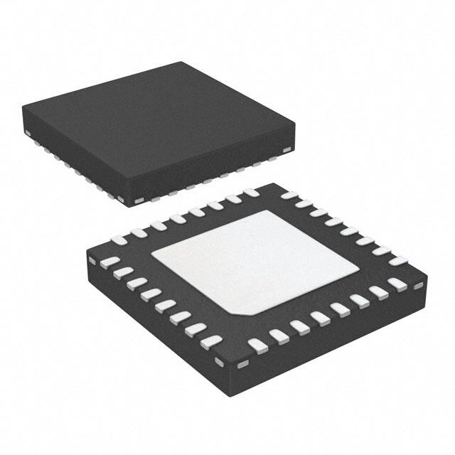


 工商网监
湘ICP备2023018690号
工商网监
湘ICP备2023018690号
