DATA SHEET
www.onsemi.com
Micro-Stepping Motor Driver
AMIS-30621
INTRODUCTION
The AMIS−30621 is a single−chip micro−stepping motor driver
with position controller and control/diagnostic interface. It is ready to
build dedicated mechatronics solutions connected remotely with a
LIN master.
The chip receives positioning instructions through the bus and
subsequently drives the motor coils to the desired position. The
on−chip position controller is configurable (OTP or RAM) for
different motor types, positioning ranges and parameters for speed,
acceleration and deceleration. The AMIS−30621 acts as a slave on the
LIN bus and the master can fetch specific status information like
actual position, error flags, etc. from each individual slave node.
The chip is implemented in I2T100 technology, enabling both high
voltage analog circuitry and digital functionality on the same chip.
The AMIS−30621 is fully compatible with the automotive voltage
requirements.
PRODUCT FEATURES
Motordriver
•
•
•
•
•
•
SOIC−20
3 & 7 SUFFIX
CASE 751AQ
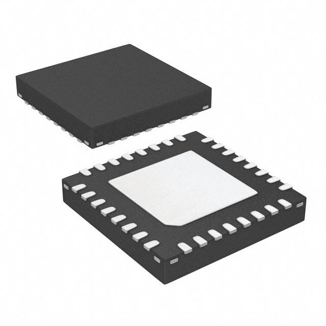
QFNW32 7x7, 0.65P
CASE 484BB
ORDERING INFORMATION
See detailed ordering and shipping information on page 2 of
this data sheet.
*For additional information on our Pb−Free strategy
and soldering details, please download the onsemi
Soldering and Mounting Techniques Reference
Manual, SOLDERRM/D.
Micro−Stepping Technology
Peak Current Up to 800 mA
Fixed Frequency PWM Current−Control
Automatic Selection of Fast and Slow Decay Mode
No External Fly−Back Diodes Required
Compliant with 14 V Automotive Systems and Industrial
Systems Up to 24 V
Power Saving
• Powerdown Supply Current < 50 mA
• 5 V Regulator with Wake−up on LIN Activity
EMI Compatibility
Controller with RAM and OTP Memory
• LIN Bus Integrated Slope Control
• HV Outputs with Slope Control
• Position Controller
• Configurable Speeds and Acceleration
• Input to Connect Optional Motion Switch
• These are Pb−Free Devices
LIN Interface
• Physical Layer Compliant to LIN rev. 2.0. Data−Link Layer
Compatible with LIN Rev. 1.3 (Note 1)
• Field−Programmable Node Addresses
• Dynamically Allocated Identifiers
• Diagnostics and Status Information
Protection
•
•
•
•
•
•
•
Overcurrent Protection
Undervoltage Management
Open−Circuit Detection
High Temperature Warning and Management
Low Temperature Flag
LIN Bus Short−Circuit Protection to Supply and Ground
Lost LIN Safe Operation
1. Minor exceptions to the conformance of the data−link layer to LIN rev. 1.3.
© Semiconductor Components Industries, LLC, 2010
January, 2022 − Rev. 5
1
Publication Order Number:
AMIS−30621/D
�AMIS−30621
APPLICATIONS
The AMIS−30621 is ideally suited for small positioning
applications. Target markets include: automotive (headlamp
alignment, HVAC, idle control, cruise control), industrial
equipment (lighting, fluid control, labeling, process control,
XYZ tables, robots...) and building automation (HVAC,
surveillance, satellite dish, renewable energy systems).
Suitable applications typically have multiple axes or require
mechatronic solutions with the driver chip mounted directly
on the motor.
Table 1. ORDERING INFORMATION
Peak Current
UV*
Package
Shipping†
AMIS30621C6213G
800 mA
High
Tube / Tray
AMIS30621C6213RG
800 mA
High
SOIC−20
(Pb−Free)
AMIS30621C6216G
800 mA
Low
AMIS30621C6216RG
800 mA
Low
AMIS30621C6217G**
800 mA
Low
AMIS30621C6217RG**
800 mA
Low
Part No.
Tape & Reel
Tube / Tray
QFNW32 7x7
(Pb−Free)
Tape & Reel
Tube / Tray
SOIC−20
(Pb−Free)
Tape & Reel
†For information on tape and reel specifications, including part orientation and tape sizes, please refer to our Tape and Reel Packaging
Specification Brochure, BRD8011/D.
*UV undervoltage lock out levels: see DC Parameters UV1 & UV2 (Stop Voltage thresholds).
** For prodcut versions AMIS30621C6217G and AMIS30621C6217RG the Ihold0 bit in OTP is programmed to ‘1’.
QUICK REFERENCE DATA
Table 2. ABSOLUTE MAXIMUM RATINGS
Symbol
Parameter
Min
Max
Unit
VBB, VHW2, VSWI
Supply voltage, Hardwired Address and SWI Pins
−0.3
+40
(Note 1)
V
Vlin
Bus input voltage
−40
+40
V
TJ
Junction temperature range (Note 2)
−50
+175
°C
Tst
Storage temperature
−55
+160
°C
Vesd
Human Body Model Electrostatic discharge voltage on LIN
pin (Note 3)
−4
+4
kV
Human Body Model Electrostatic discharge voltage on other
pins (Note 3)
−2
+2
kV
CDM Electrostatic discharge voltage on other pins (Note 4)
−500
+500
V
Stresses exceeding those listed in the Maximum Ratings table may damage the device. If any of these limits are exceeded, device functionality
should not be assumed, damage may occur and reliability may be affected.
1. For limited time: VBB < 0.5 s, SWI and HW2 pins < 1.0 s.
2. The circuit functionality is not guaranteed.
3. Human Body Model according to MIL−STD−883 Method 3015.7, measured on SOIC devices, and according to AEC−Q100:
EIA−JESD22−A114−B (100 pF via 1.5 kW) measured on QFNW device.
4. CDM according to EOS_ESD−DS5.3−1993 (draft)−socketed mode, measured on SOIC devices, and according to AEC−Q100:
EIA−JESD22−A115−A measured on QFNW devices.
Table 3. OPERATING RANGES
Symbol
Parameter
Min
Max
Unit
VBB
Supply voltage
+6.5
+29
V
TJ
Operating temperature range (Note 5)
−40
+165
°C
5. Note that the thermal warning and shutdown will get active at the level specified in the “DC Parameters”. No more than 100 cumulated hours
in life time above Ttw.
www.onsemi.com
2
�AMIS−30621
Table of Contents
General Description . . . . . . . . . . . . . . . . . . . . . . . . . . . . . . . . . . . . . . . . . . . . . . . . . . . . . . . . . . . . . . . . . . . . . . . . . . . . . . . . . . . . . . 1
Product Features . . . . . . . . . . . . . . . . . . . . . . . . . . . . . . . . . . . . . . . . . . . . . . . . . . . . . . . . . . . . . . . . . . . . . . . . . . . . . . . . . . . . . . . . 1
Applications . . . . . . . . . . . . . . . . . . . . . . . . . . . . . . . . . . . . . . . . . . . . . . . . . . . . . . . . . . . . . . . . . . . . . . . . . . . . . . . . . . . . . . . . . . . . . 2
Ordering Information . . . . . . . . . . . . . . . . . . . . . . . . . . . . . . . . . . . . . . . . . . . . . . . . . . . . . . . . . . . . . . . . . . . . . . . . . . . . . . . . . . . . . 2
Quick Reference Data . . . . . . . . . . . . . . . . . . . . . . . . . . . . . . . . . . . . . . . . . . . . . . . . . . . . . . . . . . . . . . . . . . . . . . . . . . . . . . . . . . . . 2
Maximum Ratings . . . . . . . . . . . . . . . . . . . . . . . . . . . . . . . . . . . . . . . . . . . . . . . . . . . . . . . . . . . . . . . . . . . . . . . . . . . . . . . . . . . . . . . . 2
Block Diagram . . . . . . . . . . . . . . . . . . . . . . . . . . . . . . . . . . . . . . . . . . . . . . . . . . . . . . . . . . . . . . . . . . . . . . . . . . . . . . . . . . . . . . . . . . 3
Pin Description . . . . . . . . . . . . . . . . . . . . . . . . . . . . . . . . . . . . . . . . . . . . . . . . . . . . . . . . . . . . . . . . . . . . . . . . . . . . . . . . . . . . . . . . . . 4
Package Thermal Resistance . . . . . . . . . . . . . . . . . . . . . . . . . . . . . . . . . . . . . . . . . . . . . . . . . . . . . . . . . . . . . . . . . . . . . . . . . . . . . 5
DC Parameters . . . . . . . . . . . . . . . . . . . . . . . . . . . . . . . . . . . . . . . . . . . . . . . . . . . . . . . . . . . . . . . . . . . . . . . . . . . . . . . . . . . . . . . . . . 6
AC Parameters . . . . . . . . . . . . . . . . . . . . . . . . . . . . . . . . . . . . . . . . . . . . . . . . . . . . . . . . . . . . . . . . . . . . . . . . . . . . . . . . . . . . . . . . . . 8
Typical Application . . . . . . . . . . . . . . . . . . . . . . . . . . . . . . . . . . . . . . . . . . . . . . . . . . . . . . . . . . . . . . . . . . . . . . . . . . . . . . . . . . . . . . . 9
Positioning Parameters . . . . . . . . . . . . . . . . . . . . . . . . . . . . . . . . . . . . . . . . . . . . . . . . . . . . . . . . . . . . . . . . . . . . . . . . . . . . . . . . . . 10
Structural Description . . . . . . . . . . . . . . . . . . . . . . . . . . . . . . . . . . . . . . . . . . . . . . . . . . . . . . . . . . . . . . . . . . . . . . . . . . . . . . . . . . . 13
Functions Description . . . . . . . . . . . . . . . . . . . . . . . . . . . . . . . . . . . . . . . . . . . . . . . . . . . . . . . . . . . . . . . . . . . . . . . . . . . . . . . . . . . 14
Lin Controller . . . . . . . . . . . . . . . . . . . . . . . . . . . . . . . . . . . . . . . . . . . . . . . . . . . . . . . . . . . . . . . . . . . . . . . . . . . . . . . . . . . . . . . . . . . 33
LIN Application Commands . . . . . . . . . . . . . . . . . . . . . . . . . . . . . . . . . . . . . . . . . . . . . . . . . . . . . . . . . . . . . . . . . . . . . . . . . . . . . . 42
SWI
AMIS−30621
LIN
BUS
Interface
Position
Controller
HW[2:0]
MOTXP
I−sense
PWM
regulator
X
MOTYP
I−sense
PWM
regulator
Y
Controller
MOTXN
TST
Decoder
Main Control
Registers
OTP − ROM
Sinewave
Table
DAC’s
4 MHz
Temp
sense
Vref
Voltage
Regulator
VBB
VDD
Oscillator
Charge Pump
CPN CPP VCP
GND
Figure 1. Block Diagram
www.onsemi.com
3
MOTYN
�AMIS−30621
HW0
1
20
SWI
HW1
2
19
VBB
3
18
MOTXP
4
17
GND
TST
5
16
MOTXN
LIN
6
GND
7
HW2
CPN
CPP
AMIS−30621
VDD
GND
15
MOTYP
14
GND
8
13
MOTYN
9
12
VBB
10
11
VCP
SOIC−20
Figure 2. SOIC−20 and QFNW32 Pin−out
Table 4. PIN DESCRIPTION
Pin Name
Pin Description
To be Tied to GND or VDD
HW0
Bit 0 of LIN−ADD
HW1
Bit 1 of LIN−ADD
VDD
Internal supply (needs external decoupling capacitor)
GND
Ground, heat sink
TST
SOIC−20
QFNW32
1
8
2
9
3
10
4,7,14,17
11, 14, 25, 26, 31, 32
Test pin (to be tied to ground in normal operation)
5
12
LIN
LIN−bus connection
6
13
HW2
Bit 2 LIN−ADD
8
15
CPN
Negative connection of pump capacitor (charge pump)
9
17
CPP
Positive connection of pump−capacitor (charge pump)
10
18
VCP
Charge−pump filter−capacitor
11
19
VBB
Battery voltage supply
12,19
3, 4, 5, 20, 21, 22
MOTYN
Negative end of phase Y coil
13
23, 24
MOTYP
Positive end of phase Y coil
15
27, 28
MOTXN
Negative end of phase X coil
16
29, 30
MOTXP
Positive end of phase X coil
18
1, 2
SWI
Switch input
20
6
NC
Not connected (to be tied to ground)
7, 16
www.onsemi.com
4
�AMIS−30621
PACKAGE THERMAL RESISTANCE
The thermal resistances are presented in Table 5: DC
Parameters.
The major thermal resistances of the device are the Rth
from the junction to the ambient (Rthja) and the overall Rth
from the junction to the leads (Rthjp).
The QFNW32 device is designed to provide superior
thermal performance. Using an exposed die pad on the
bottom surface of the package, is mainly contributing to this
performance. In order to take full advantage of the exposed
pad, it is most important that the PCB has features to conduct
heat away from the package. A thermal grounded pad with
thermal vias can achieve this.
In below table, one can find the values for the Rthja and
Rthjp, simulated according to the JESD−51standard:
The AMIS−30621 is available in SOIC−20 and optimized
QFNW32 packages. For cooling optimizations, the
QFNW32 has an exposed thermal pad which has to be
soldered to the PCB ground plane. The ground plane needs
thermal vias to conduct the head to the bottom layer.
Figures 3 and 4 give examples for good power distribution
solutions.
For precise thermal cooling calculations the major
thermal resistances of the devices are given. The thermal
media to which the power of the devices has to be given are:
• Static environmental air (via the case)
• PCB board copper area (via the device pins and
exposed pad)
Package
Rth
Junction−to−Leads and
Exposed Pad (Rthjp)
Rth
Junction−to−Leads
(Rthjp)
Rth
Junction−to−Ambient
Rthja 1S0P
Rth
Junction−to−Ambient
Rthja 2S2P
19
62
39
60
30
SOIC−20
QFNW32
0.95
The Rthja for 2S2P is simulated conform to JESD−51 as
follows:
• A 4−layer printed circuit board with inner power planes
and outer (top and bottom) signal layers is used
• Board thickness is 1.46 mm (FR4 PCB material)
• The 2 signal layers: 70 mm thick copper with an area of
5500 mm2 copper and 20% conductivity
• The 2 power internal planes: 36 mm thick copper with
an area of 5500 mm2 copper and 90% conductivity
The Rthja for 1S0P is simulated conform to JESD−51 as
follows:
• A 1−layer printed circuit board with only 1 layer
• Board thickness is 1.46 mm (FR4 PCB material)
• The layer has a thickness of 70 mm copper with an area
of 5500 mm2 copper and 20% conductivity
ÎÎÎÎÎÎÎÎÎÎÎÎ
ÎÎÎÎÎÎÎÎÎÎÎÎ
ÎÎÎÎÎÎÎÎÎÎÎÎ
ÌÌ
ÎÎÎÎÎÎÎÎÎÎÎÎ
ÌÌ
ÎÎÎÎÎÎÎÎÎÎÎÎ
ÌÌ
ÎÎÎÎÎÎÎÎÎÎÎÎ
ÎÎÎÎÎÎÎÎÎÎÎÎ
SOIC−20
ÎÎÎÎÎÎÎÎÎÎÎÎÎ
ÎÎÎÎÎÎÎÎÎÎÎÎÎ
ÎÎÎÎÎÎÎÎÎÎÎÎÎ
ÎÎÎÎÎÎÎÎÎÎÎÎÎ
ÎÎÎÎÎÎÎÎÎÎÎÎÎ
ÎÎÎÎÎÎÎÎÎÎÎÎÎ
ÎÎÎÎÎÎÎÎÎÎÎÎÎ
QFNW32
Figure 4. Example of QFNW32 PCB Ground Plane
Layout (Preferred Layout at Top and Bottom)
Figure 3. Example of SOIC−20 PCB Ground Plane
Layout (Preferred Layout at Top and Bottom)
www.onsemi.com
5
�AMIS−30621
DC PARAMETERS
The DC parameters are guaranteed over temperature and VBB in the operating range, unless otherwise specified. Convention:
currents flowing into the circuit are defined as positive.
Table 5. DC PARAMETERS
Symbol
Pins
Parameter
Test Conditions
Min
Typ
Max
Unit
MOTORDRIVER
IMSmax,Peak
Max current through motor
coil in normal operation
VBB = 14 V
800
mA
IMSmax,RMS
Max RMS Current Through
Coil in Normal Operation
VBB = 14 V
570
mA
Absolute Error on Coil Current
(Note 6)
VBB = 14 V
−10
Matching of X and Y Coil
Currents
VBB = 14 V
−7
IMSabs
IMSrel
RDS(on)
MOTXP
MOTXN
MOTYP
MOTYN
IMSL
On Resistance for Each Motor
Pin at IMSmax (Note 7)
Pull down current
10
%
0
7
%
VBB = 12 V, TJ = 50°C
0.50
1
W
VBB = 8 V, TJ = 50°C
0.55
1
W
VBB = 12 V, TJ = 150°C
0.70
1
W
VBB = 8 V, TJ = 150°C
0.85
1
W
2.2
mA
HiZ Mode, VBB = 7.7 V
0.4
−1
LIN TRANSMITTER
Ibus_off
Dominant State, Driver Off
Vbus = 0 V, VBB = 8 V and 18 V
Ibus_off
Recessive State, Driver Off
Vbus = Vbat,
VBB = 8 V and 18 V
Ibus_lim
Current Limitation
VBB = 8 V and 18 V
50
Rslave
Pullup Resistance
VBB = 8 V and 18 V
20
Vbus_dom
Receiver Dominant State
VBB = 8 V and 18 V
Vbus_rec
Receiver Recessive State
VBB = 8 V and 18 V
Receiver Hysteresis
VBB = 8 V and 18 V
0.05 * VBB
LIN
mA
20
mA
75
130
mA
30
47
kW
0
0.4 * VBB
V
0.6 * VBB
VBB
V
0.175 * VBB
V
152
°C
LIN RECEIVER
LIN
Vbus_hys
THERMAL WARNING AND SHUTDOWN
Ttw
Thermal warning
Ttsd
Thermal shutdown
(Notes 8 and 9)
Ttw + 10
°C
Tlow
Low temperature warning
(Note 9)
Ttw − 152
°C
138
145
SUPPLY AND VOLTAGE REGULATOR
VBBOTP
Supply voltage for OTP
zapping (Note 10)
UV1
Stop voltage high threshold
UV2
Stop voltage low threshold
UV1
Stop voltage high threshold
VBB
UV2
Stop voltage low threshold
Ibat
Total current consumption
Ibat_s
Sleep mode current
consumption
VDD
Regulated internal supply
(Note 11)
VDDReset
IDDLim
VDD
9.0
Product versions with low UV;
See Ordering Information
Product versions with high UV;
See Ordering Information
Unloaded outputs
VBB = 29 V
Digital supply reset level @
powerdown (Note 12)
Current limitation
Pin shorted to ground
VBB = 14 V
www.onsemi.com
6
V
7.7
8.3
8.9
V
7.0
7.5
8.0
V
8.8
9.3
9.8
V
8.1
8.5
8.9
V
1
3.50
10.0
mA
40
100
mA
5
5.25
V
4.5
V
40
mA
VBB = 8 V and 18 V
8 V < VBB < 29 V
10.0
4.75
�AMIS−30621
Table 5. DC PARAMETERS
Symbol
Pins
Parameter
Test Conditions
Min
Typ
Max
Unit
SWITCH INPUT AND HARDWIRE ADDRESS INPUT
Rt_OFF
Rt_ON
Switch OPEN Resistance
(Note 13)
Switch ON Resistance
SWI HW2 (Note 13)
VBB_sw
VBB range for guaranteed
operation of SWI and HW2
Ilim_sw
Current limitation
10
kW
Switch to GND or VBB
6
Short to GND or Vbat
VBB = 29 V
2
kW
29
V
45
mA
HARDWIRED ADDRESS INPUTS AND TEST PIN
Vhigh
Vlow
HWhyst
Input level high
HW0
Input level low
HW1 TST
Hysteresis
VBB = 14 V
0.7 * VDD
V
VBB = 14 V
VBB = 14 V
0.3 * VDD
0.075 * VDD
V
V
CHARGE PUMP
Output voltage
VCP
VCP
7 V < VBB v 14 V
14 V < VBB
2 * VBB −
2.5
V
VBB + 10
VBB + 15
V
Cbuffer
External buffer capacitor
220
470
nF
Cpump
CPP CPN External pump capacitor
220
470
nF
PACKAGE THERMAL RESISTANCE VALUES
Rthja
SO
Thermal resistance
junction−to−ambient (2S2P)
39
K/W
Rthjp
SO
Thermal resistance
junction−to−leads
19
K/W
Rthja
NQ
Thermal resistance
junction−to−ambient (2S2P)
30
K/W
NQ
Thermal resistance
junction−to−leads and
exposed pad
0.95
K/W
Rthjp
Simulated conform JEDEC
JES.D51
6. Tested in production for 800 mA, 400 mA, 200 mA and 100 mA current settings for both X and Y coil.
7. Based on characterization data.
8. No more than 100 cumulated hours in life time above Ttw.
9. Thermal shutdown and low temperature warning are derived from thermal warning. Guaranteed by design.
10. A buffer capacitor of minimum 100 mF is needed between VBB and GND. Short connections to the power supply are recommended.
11. Pin VDD must not be used for any external supply
12. The RAM content will not be altered above this voltage.
13. External resistance value seen from pin SWI or HW2, including 1 kW series resistor. For the switch OPEN, the maximum allowed leakage
current is represented by a minimum resistance seen from the pin.
www.onsemi.com
7
�AMIS−30621
AC PARAMETERS
The AC parameters are guaranteed for temperature and VBB in the operating range unless otherwise specified.
The LIN transmitter and receiver physical layer parameters are compliant to LIN rev. 2.0 & 2.1.
Table 6. AC PARAMETERS
Symbol
Pins
Parameter
Test Conditions
Min
Typ
Max
Unit
10
ms
4.4
MHz
POWERUP
Powerup Time
Tpu
Guaranteed by Design
INTERNAL OSCILLATOR
Frequency of Internal Oscillator
fosc
VBB = 14 V
3.6
4.0
LIN TRANSMITTER CHARACTERISTICS ACCORDING TO LIN V2.0 & V2.1
D1
D2
LIN
Duty Cycle 1 = tBus_rec(min)/
(2 x tBit); See Figure 5
THRec(max)= 0.744 x VBB
THDom(max)= 0.581 x VBB;
VBB = 7.0 V...18 V; tBit =
50 ms
Duty Cycle 2 = tBus_rec(max)/
(2 x tBit); See Figure 5
THRec(min)= 0.284 x VBB
THDom(min)= 0.422 x VBB;
VBB = 7.6 V...18 V;
tBit = 50 ms
0.396
0.581
LIN RECEIVER CHARACTERISTICS ACCORDING TO LIN V2.0 & V2.1
trx_pdr
trx_pdf
LIN
trx_sym
Propagation delay bus dominant VBB = 7.0 V & 18 V;
to RxD = Low
See Figure 5
6
ms
Propagation delay bus recessive to RxD = High
VBB = 7.0 V & 18 V;
See Figure 5
6
ms
Symmetry of receiver propagation delay
trx_pdr – trx_pdf
+2
ms
−2
SWITCH INPUT AND HARDWIRE ADDRESS INPUT
Tsw
Tsw_on
SWI
HW2
Scan pulse period (Note 14)
VBB = 14 V
1024
ms
Scan pulse duration (Note 14)
VBB = 14 V
64
ms
MOTORDRIVER
PWM frequency (Note 14)
Fpwm
Tbrise
Tbfall
Turn−on transient time
MOTxx
Tstab
Turn−off transient time
18
Between 10% and 90%
VBB = 14 V
Run current stabilization time
(Note 14)
20
22.0
kHz
150
ns
140
ns
1/Vmin
s
250
kHz
CHARGE PUMP
fCP
CPN
CPP
Charge pump frequency
(Note 14)
VBB = 14 V
14. Derived from the internal oscillator
www.onsemi.com
8
�AMIS−30621
TxD
tBIT
tBIT
50%
t
tBUS_dom(max)
LIN
tBUS_rec(min)
THRec(max)
THDom(max)
Thresholds
receiver 1
THRec(min)
THDom(min)
Thresholds
receiver 2
t
tBUS_dom(min)
RxD
tBUS_rec(max)
(receiver 2)
50%
trx_pdf
trx_pdr
t
Figure 5. Timing Diagram for AC Characteristics According to LIN 2.0 & 2.1
TYPICAL APPLICATION
VBAT
C8
100 nF
C7
100 mF
C5
CPN
VDD
1 mF
C9
HW0
HW1
Connect
to VBAT
or GND
1 kW
C1
HW2
C6
220 nF
CPP VCP
10
9
3
C4
C3
220 nF
VBB
VBB
11
19
20
12
1
18
AMIS−30621
2
LIN
VDR 27 V
C10
8
15
13
6
5
4
7
1k
SWI
C2
2.7 nF
MOTXP
14
MOTYP
MOTYN
17
TST
GND
Figure 6. Typical Application Diagram for SO device.
1.
2.
3.
4.
5.
6.
7.
All resistors are ±5%, 1/4 W
C1, C2 minimum value is 2.7 nF, maximum value is 10 nF
Depending on the application, the ESR value and working voltage of C7 must be carefully chosen
C3 and C4 must be close to pins VBB and GND
C5 and C6 must be as close as possible to pins CPN, CPP, VCP, and VBB to reduce EMC radiation
C9 must be a ceramic capacitor to assure low ESR
C10 is placed for EMC reasons; value depends on EMC requirements of the application
www.onsemi.com
9
Connect
to VBAT
or GND
16 MOTXN
2.7 nF
LIN bus
100 nF
100 nF
M
�AMIS−30621
POSITIONING PARAMETERS
Stepping Modes
Maximum Velocity
One of four possible stepping modes can be programmed:
• Half−stepping
• 1/4 micro−stepping
• 1/8 micro−stepping
• 1/16 micro−stepping
For each stepping mode, the maximum velocity Vmax can
be programmed to 16 possible values given in the table
below.
The accuracy of Vmax is derived from the internal
oscillator. Under special circumstances it is possible to
change the Vmax parameter while a motion is ongoing. All
16 entries for the Vmax parameter are divided into four
groups. When changing Vmax during a motion the
application must take care that the new Vmax parameter
stays within the same group.
Table 7. MAXIMUM VELOCITY SELECTION TABLE
Vmax index
Stepping mode
Group
Half−stepping
(half−step/s)
1/4th
Micro−stepping
(micro−step/s)
1/8th
Micro−stepping
(micro−step/s)
1/16th
Micro−stepping
(micro−step/s)
A
197
395
790
1579
Hex
Dec
Vmax
(full step/s)
0
0
99
1
1
136
273
546
1091
2182
2
2
167
334
668
1335
2670
3
3
197
395
790
1579
3159
4
4
213
425
851
1701
3403
5
5
228
456
912
1823
3647
6
6
243
486
973
1945
3891
7
7
273
546
1091
2182
4364
8
8
303
607
1213
2426
4852
668
1335
2670
5341
729
1457
2914
5829
B
9
9
334
A
10
364
B
11
395
790
1579
3159
6317
C
12
456
912
1823
3647
7294
D
13
546
1091
2182
4364
8728
E
14
729
1457
2914
5829
11658
F
15
973
1945
3891
7782
15564
C
D
www.onsemi.com
10
�AMIS−30621
Minimum Velocity
Once the maximum velocity is chosen, 16 possible values can be programmed for the minimum velocity Vmin. The table
below provides the obtainable values in full−step/s. The accuracy of Vmin is derived from the internal oscillator.
Table 8. OBTAINABLE VALUES IN FULL−STEP/S FOR THE MINIMUM VELOCITY
Vmax (Full−step/s)
A
Vmin Index
B
C
D
Hex
Dec
Vmax Factor
99
136
167
197
213
228
243
273
303
334
364
395
456
546
729
973
0
0
1
99
136
167
197
213
228
243
273
303
334
364
395
456
546
729
973
1
1
1/32
3
4
5
6
6
7
7
8
8
10
10
11
13
15
19
27
2
2
2/32
6
8
10
11
12
13
14
15
17
19
21
23
27
31
42
57
3
3
3/32
9
12
15
18
19
21
22
25
27
31
32
36
42
50
65
88
4
4
4/32
12
16
20
24
26
28
30
32
36
40
44
48
55
65
88
118
5
5
5/32
15
21
26
31
32
35
37
42
46
51
55
61
71
84
111
149
6
6
6/32
18
25
31
36
39
42
45
50
55
61
67
72
84
99
134
179
7
7
7/32
21
30
36
43
46
50
52
59
65
72
78
86
99
118
156
210
8
8
8/32
24
33
41
49
52
56
60
67
74
82
90
97
113
134
179
240
9
9
9/32
28
38
47
55
59
64
68
76
84
93
101
111
128
153
202
271
A
10
10/32
31
42
51
61
66
71
75
84
93
103
113
122
141
168
225
301
B
11
11/32
34
47
57
68
72
78
83
93
103
114
124
135
156
187
248
332
C
12
12/32
37
51
62
73
79
85
91
101
113
124
135
147
170
202
271
362
D
13
13/32
40
55
68
80
86
93
98
111
122
135
147
160
185
221
294
393
E
14
14/32
43
59
72
86
93
99
106
118
132
145
158
172
198
237
317
423
F
15
15/32
46
64
78
93
99
107
113
128
141
156
170
185
214
256
340
454
NOTES: The Vmax factor is an approximation.
In case of motion without acceleration (AccShape = 1) the length of the steps = 1/Vmin. In case of accelerated motion
(AccShape = 0) the length of the first step is shorter than 1/Vmin depending of Vmin, Vmax and Acc.
www.onsemi.com
11
�AMIS−30621
Acceleration and Deceleration
combinations of acceleration index and maximum speed
(gray cells).
The accuracy of Acc is derived from the internal
oscillator.
Sixteen possible values can be programmed for Acc
(acceleration and deceleration between Vmin and Vmax).
The table below provides the obtainable values in
full−step/s2. One observes restrictions for some
Table 9. ACCELERATION AND DECELERATION SELECTION TABLE
Vmax (FS/s) →
99
136
167
197
213
228
243
273
303
334
364
395
456
546
729
973
↓ Acc Index
Acceleration (Full−step/s2)
Hex
Dec
0
0
1
1
2
2
1004
3
3
3609
4
4
6228
5
5
8848
6
6
11409
7
7
13970
8
8
16531
9
9
19092
A
10
21886
B
11
24447
C
12
D
13
E
14
F
15
49
106
473
27008
29570
29570
34925
40047
Positioning
The formula to compute the number of equivalent
full−steps during acceleration phase is:
Nstep +
735
14785
218
V max
The position programmed in commands SetPosition
and SetPositionShort is given as a number of
(micro−)steps. According to the chosen stepping mode, the
position words must be aligned as described in the table
below. When using command SetPositionShort or
GotoSecurePosition, data is automatically aligned.
2 * V min 2
2
Acc
Table 10. POSITION WORD ALIGNMENT
Stepping Mode
Position Word: Pos[15:0]
Shift
1/16th
S
B14 B13 B12 B11 B10
B9
B8
B7
B6
B5
B4
B3
B2
B1
LSB
No shift
1/8th
S
B13 B12 B11 B10
B9
B8
B7
B6
B5
B4
B3
B2
B1
LSB
0
1−bit left ⇔ ×2
1/4th
S
B12 B11 B10
B9
B8
B7
B6
B5
B4
B3
B2
B1
LSB
0
0
2−bit left ⇔ ×4
Half−stepping
S
B11 B10
B9
B8
B7
B6
B5
B4
B3
B2
B1
LSB
0
0
0
3−bit left ⇔ ×8
PositionShort
S
S
S
B9
B8
B7
B6
B5
B4
B3
B2
B1
LSB
0
0
0
No Shift
SecurePosition
S
B9
B8
B7
B6
B5
B4
B3
B2
B1
LSB
0
0
0
0
0
No shift
NOTES: LSB: Least Significant Bit
S: Sign bit, two’s complement
www.onsemi.com
12
�AMIS−30621
Position Ranges
A position is coded by using the binary two’s complement format. According to the positioning commands used and to the
chosen stepping mode, the position range will be as shown in the following table.
Table 11. POSITION RANGE
Command
SetPosition
Stepping Mode
Position Range
Full Range Excursion
Number of Bits
Half−stepping
−4096 to +4095
8192 half−steps
13
1/4th
micro−stepping
−8192 to +8191
16384 micro−steps
14
1/8th
micro−stepping
−16384 to +16383
32768 micro−steps
15
−32768 to +32767
65536 micro−steps
16
−1024 to +1023
2048 half−steps
11
1/16th
SetPositionShort
micro−stepping
Half−stepping
Secure Position
When using the command SetPosition, although
coded on 16 bits, the position word will have to be shifted to
the left by a certain number of bits, according to the stepping
mode.
A secure position can be programmed. It is coded in
11−bits, thus having a lower resolution than normal
positions, as shown in the following table. See also
command GotoSecurePosition and LIN lost
behavior.
Table 12. SECURE POSITION
Stepping Mode
Secure Position Resolution
Half−stepping
4 half−steps
1/4th
micro−stepping
8 micro−steps (1/4th)
1/8th micro−stepping
16 micro−steps (1/8th)
1/16th micro−stepping
32 micro−steps (1/16th)
Important
NOTES: The secure position is disabled in case the programmed value is the reserved code “10000000000” (0x400 or most negative
position).
At start up the OTP register is copied in RAM as illustrated below.
SecPos10
SecPos9
SecPos8
SecPos2
SecPos1
SecPos0
RAM
SecPos10
SecPos9
SecPos8
SecPos2
SecPos1
SecPos0
OTP
• Shaft = 0 ⇒ MOTXP is used as positive pin of the X
Shaft
A shaft bit, which can be programmed in OTP or with
command SetMotorParam, defines whether a positive
motion is a clockwise (CW) or counter−clockwise rotation
(CCW) (an outer or an inner motion for linear actuators):
coil, while MOTXN is the negative one.
• Shaft = 1 ⇒ opposite situation.
STRUCTURAL DESCRIPTION
See also the Block Diagram in Figure 1.
Stepper Motordriver
The Motor driver receives the control signals from the
control logic. The main features are:
• Two H−bridges, designed to drive a stepper motor with
two separated coils. Each coil (X and Y) is driven by
one H−bridge, and the driver controls the currents
flowing through the coils. The rotational position of the
•
rotor, in unloaded condition, is defined by the ratio of
current flowing in X and Y. The torque of the stepper
motor when unloaded is controlled by the magnitude of
the currents in X and Y.
The control block for the H−bridges, including the
PWM control, the synchronous rectification and the
internal current sensing circuitry.
www.onsemi.com
13
�AMIS−30621
• The charge pump to allow driving of the H−bridges’
LIN Interface
The LIN interface implements the physical layer and the
MAC and LLC layers according to the OSI reference model.
It provides and gets information to and from the control logic
block, in order to drive the stepper motor, to configure the
way this motor must be driven, or to get information such as
actual position or diagnosis (temperature, battery voltage,
electrical status...) and pass it to the LIN master node.
high side transistors.
• Two pre−scale 4−bit DAC’s to set the maximum
magnitude of the current through X and Y.
• Two DAC’s to set the correct current ratio through X
and Y.
Battery voltage monitoring is also performed by this
block, which provides the required information to the
control logic part. The same applies for detection and
reporting of an electrical problem that could occur on the
coils or the charge pump.
Miscellaneous
The AMIS−30621 also contains the following:
• An internal oscillator, needed for the LIN protocol
handler as well as the control logic and the PWM
control of the motor driver.
• An internal trimmed voltage source for precise
referencing.
• A protection block featuring a thermal shutdown and a
power−on−reset (POR) circuit.
• A 5 V regulator (from the battery supply) to supply the
internal logic circuitry.
Control Logic (Position Controller and Main Control)
The control logic block stores the information provided by
the LIN interface (in a RAM or an OTP memory) and
digitally controls the positioning of the stepper motor in
terms of speed and acceleration, by feeding the right signals
to the motor driver state machine.
It will take into account the successive positioning
commands to properly initiate or stop the stepper motor in
order to reach the set point in a minimum time.
It also receives feedback from the motor driver part in
order to manage possible problems and decide on internal
actions and reporting to the LIN interface.
FUNCTIONS DESCRIPTION
Position Controller
This chapter describes the following functional blocks in
more detail:
• Position controller
• Main control and register, OTP memory + ROM
• Motor driver
The LIN controller is discussed in a separate chapter.
ÑÑ
ÑÑ
ÑÑ
ÑÑ
ÑÑ
ÑÑ
ÑÑ
ÑÑ
ÑÑ
ÑÑ
Positioning and Motion Control
A positioning command will produce a motion as
illustrated in Figure 7. A motion starts with an acceleration
phase from minimum velocity (Vmin) to maximum velocity
(Vmax) and ends with a symmetrical deceleration. This is
defined by the control logic according to the position
required by the application and the parameters programmed
by the application during the configuration phase. The
current in the coils is also programmable.
Velocity
Acceleration
range
Deceleration
range
Vmax
Zero Speed
Hold Current
ÑÑ
ÑÑ
ÑÑ
ÑÑ
ÑÑ
ÑÑ
ÑÑ
ÑÑ
ÑÑ
ÑÑ
Zero Speed
Hold Current
Vmin
Position
Pstart
P=0
Pmin
Pstop
Pmax
Figure 7. Positioning and Motion Control
www.onsemi.com
14
�AMIS−30621
Table 13. POSITION RELATED PARAMETERS
Parameter
Reference
Pmax – Pmin
See Positioning
Zero Speed Hold Current
See Ihold
Maximum Current
See Irun
Acceleration and Deceleration
See Acceleration and Deceleration
Vmin
See Minimum Velocity
Vmax
See Maximum Velocity
Different positioning examples are shown in the table below.
Table 14. POSITIONING EXAMPLES
Short motion.
Velocity
time
New positioning command in same direction, shorter or longer, while a motion
is running at maximum velocity.
Velocity
time
New positioning command in same direction while in deceleration phase
(Note 15)
Note: there is no wait time between the
deceleration phase and the new acceleration phase.
Velocity
New positioning command in reverse
direction while motion is running at maximum velocity.
Velocity
time
time
New positioning command in reverse
direction while in deceleration phase.
Velocity
time
New velocity programming while motion
is running.
Velocity
time
15. Reaching the end position is always guaranteed, however velocity rounding errors might occur after consecutive accelerations during a
deceleration phase. The velocity rounding error will be removed at Vmin (e.g. at end of acceleration or when AccShape=1).
www.onsemi.com
15
�AMIS−30621
Dual Positioning
Then a second motion to a position Pos2[15:0] is done
at the specified Vmin velocity in the SetDualPosition
command (no acceleration). Once the second motion is
achieved, the ActPos register is reset to zero, whereas
TagPos register is not changed.
A SetDualPosition command allows the user to
perform a positioning using two different velocities. The
first motion is done with the specified Vmin and Vmax
velocities in the SetDualPosition command, with the
acceleration (deceleration) parameter already in RAM, to a
position
Pos1[15:0]
also
specified
in
SetDualPosition.
A new motion will
start here
Depends on
AccShape
Vmax
Profile:
Vmin
second
movement
first movement
27 ms
Motion status:
00
0
0
00
0
5 steps
100 101
xx
Pos: xx
0
00
During one Vmin time the
ActPos is 100
Position:
27 ms
Secure
positioning
(if enabled)
ActPos: 100 ActPos: 100
104 105
105 0
ActPos:0
60
ActPos: 60
Assume:
First Position = 100
Second Position = 105
Secure Position = 60
ResetPos
Figure 8. Dual Positioning
Remark: This operation cannot be interrupted or influenced by any further command unless the occurrence of the conditions
driving to a motor shutdown or by a HardStop command. Sending a SetDualPosition command while a motion is
already ongoing is not recommended. After dual positioning is executed the internal flag “Reference done” is set.
1. The priority encoder is describing the management of states and commands.
2. If a SetPosition(Short) command issued during a DualPosition sequence, it will be kept in position buffer memory
and executed afterwards. This applies also for the commands sleep, SetMotorParam and GotoSecurePosition.
3. Commands such as GetActualPos or GetStatus will be executed while a dual positioning is running. This applies also
for a dynamic ID assignment LIN frame.
4. A DualPosition sequence starts by setting TagPos buffer register to SecPos value, provided secure position is enabled
otherwise TagPos is reset to zero.
5. The acceleration/deceleration value applied during a DualPosition sequence is the one stored in RAM before the
SetDualPosition command is sent. The same applies for shaft bit, but not for Irun, Ihold and StepMode, which
can be changed during the dual positioning sequence.
6. The Pos1, Pos2, Vmax and Vmin values programmed in a SetDualPosition command apply only for this
sequence. All further positioning will use the parameters stored in RAM (programmed for instance by a former
SetMotorParam command).
7. Commands ResetPosition, SetDualPosition and SoftStop will be ignored while a DualPosition sequence is ongoing,
and will not be executed afterwards.
8. A SetMotorParam command should not be sent during a SetDualPosition sequence.
9. If for some reason ActPos equals Pos1[15:0] at the moment the SetDualPosition command is issued, the
circuit will enter in deadlock state. Therefore, the application should check the actual position by a GetPosition or a
GetFullStatus command prior to send the SetDualPosition command.
www.onsemi.com
16
�AMIS−30621
Position Periodicity
Hardwired Address HW2
In the drawing below, a simplified schematic diagram is
shown of the HW2 comparator circuit.
The HW2 pin is sensed via 2 switches. The DriveHS and
DriveLS control lines are alternatively closing the top and
bottom switch connecting HW2 pin with a current to resistor
converter. Closing STOP (DriveHS = 1) will sense a current
to GND. In that case the top I³ R converter output is low,
via the closed passing switch SPASS_T this signal is fed to the
“R” comparator which output HW2_Cmp is high. Closing
bottom switch SBOT (DriveLS = 1) will sense a current to
VBAT. The corresponding I³ R converter output is low and
via SPASS_B fed to the comparator. The output HW2_Cmp
will be high.
Depending on the stepping mode the position can range
from –4096 to +4095 in half−step to –32768 to +32767 in
1/16th micro−stepping mode. One can project all these
positions lying on a circle. When executing the command
SetPosition, the position controller will set the
movement direction in such a way that the traveled distance
is minimal.
The figure below illustrates that the moving direction
going from ActPos = +30000 to TagPos = –30000 is
clockwise.
If a counter clockwise motion is required in this example,
several consecutive SetPosition commands can be
used.
+10000
+20000
ActPos = +30000
0
Motion direction
TagPos = −30000
−10000
−20000
Figure 9. Motion Direction is Function of Difference
between ActPos and TagPos
SPASS_T
I→R
State
1 kW
HW2
SBOT
1
2
1 = R2GND
2 = R2VBAT
3 = OPEN
High
DriveHS
STOP
Low
LOGIC
DriveLS
3
‘‘R”−Comp
I/R
SPASS_B
Debouncer
COMP
Rth
32 ms
HW2_Cmp
Figure 10. Simplified Schematic Diagram of the HW2 Comparator
3 cases can be distinguished (see also Figure 10 above):
• HW2 is connected to ground: R2GND or drawing 1
• HW2 is connected to VBAT: R2VBAT or drawing 2
• HW2 is floating: OPEN or drawing 3
www.onsemi.com
17
Float
�AMIS−30621
Table 15. STATE DIAGRAM OF THE HW2 COMPARATOR
Previous
State
DriveLS
DriveHS
HW2_Cmp
New State
Condition
Drawing
Float
1
0
0
Float
R2GND or OPEN
1 or 3
Float
1
0
1
High
R2VBAT
2
Float
0
1
0
Float
R2VBAT or OPEN
2 or 3
Float
0
1
1
Low
R2GND
1
Low
1
0
0
Low
R2GND or OPEN
1 or 3
Low
1
0
1
High
R2VBAT
2
Low
0
1
0
Float
R2VBAT or OPEN
2 or 3
Low
0
1
1
Low
R2GND
1
High
1
0
0
Float
R2GND or OPEN
1 or 3
High
1
0
1
High
R2VBAT
2
High
0
1
0
High
R2VBAT or OPEN
2 or 3
High
0
1
1
Low
R2GND
1
As illustrated in the table above (Table 15), the state is
depending on the previous state, the condition of the 2
switch controls (DriveLS and DriveHS) and the output of
HW2_Cmp. The figure below is showing an example of a
practical case where a connection to VBAT is interrupted.
The logic is controlling the correct sequence in closing the
switches and in interpreting the 32 ms debounced
HW2_Cmp output accordingly. The output of this small
state−machine is corresponding to:
• High or address = 1
• Low or address = 0
• Floating
www.onsemi.com
18
�AMIS−30621
Condition
R2 VBAT
OPEN
R2 VBAT
R2 GND
t
Tsw = 1024 ms
DriveLS
t
Tsw_on = 64 ms
DriveHS
t
“R”−Comp
Rth
t
HW2_Cmp
t
Low
High
Float
High
Float
State
t
Figure 11. Timing Diagram Showing the Change in States for HW2 Comparator
R2VBAT
will be low. The previous state was high. Based on Table 15
one can see that the state changes to float. This will trigger
a motion to secure position.
A resistor is connected between VBAT and HW2. Every
1024 ms SBOT is closed and a current is sensed. The output
of the I → R converter is low and the HW2_Cmp output is
high. Assuming the previous state was floating, the internal
logic will interpret this as a change of state and the new state
will be high (see also Table 15). The next time SBOT is
closed the same conditions are observed. The previous state
was high, so based on Table 15 the new state remains
unchanged. This high state will be interpreted as HW2
address = 1.
R2GND
If a resistor is connected between HW2 and the GND, a
current is sensed every 1024 ms when STOP is closed. The
output of the top I → R converter is low and as a result the
HW2_Cmp output switches to high. Again based on the
stated diagram in Table 15 one can see that the state will
change to Low. This low state will be interpreted as HW2
address = 0.
External Switch SWI
As illustrated in Figure 12 the SWI comparator is almost
identical to HW2. The major difference is in the limited
number of states. Only open or closed is recognised leading
to respectively ESW = 0 and ESW = 1.
OPEN
In case the HW2 connection is lost (broken wire, bad
contact in connector) the next time SBOT is closed, this will
be sensed. There will be no current, the output of the
corresponding I → R converter is high and the HW2_Cmp
www.onsemi.com
19
�AMIS−30621
SPASS_T
I→R
State
DriveHS
STOP
1 kW
Closed
LOGIC
SWI
DriveLS
Open
SBOT
1
2
3
‘‘R”−Comp
1 = R2GND
2 = R2VBAT
3 = OPEN
I/R
SPASS_B
COMP
32 ms Debouncer
SWI_Cmp
Rth
Figure 12. Simplified Schematic Diagram of the SWI Comparator
As illustrated in the drawing above, a change in state is
always synchronized with DriveHS or DriveLS. The same
synchronization is valid for updating the internal position
register. This means that after every current pulse (or closing
of STOP or SBOT) the state of the position switch together
with the corresponding position is memorized.
The GetActualPos command reads back the
register and the status of ESW. In this way the master node
may get synchronous information about the state of the
switch together with the position of the motor. See Table 16
below.
Table 16. GetActualPos LIN COMMAND
Reading Frame
Structure
Byte
Content
Bit 7
Bit 6
Bit 5
Bit 4
Bit 3
Bit 2
Bit 1
Bit 0
0
Identifier
*
*
1
0
ID3
ID2
ID1
ID0
1
Data 1
ESW
2
Data 2
3
Data 3
4
Data 4
5
Checksum
AD[6:0]
ActPos[15:8]
ActPos[7:0]
VddReset
StepLoss
ElDef
UV2
TSD
Checksum over data
www.onsemi.com
20
TW
Tinfo[1:0]
�AMIS−30621
DriveHS
512 ms
Tsw = 1024 ms
t
Tsw_on = 64 ms
DriveLS
t
“R”−Comp
Rth
t
SWI_Cmp
60 ms
t
ESW
0
1
1
1
ActPos + 3
ActPos + 2
ActPos
ActPos
ActPos + 1
t
t
Figure 13. Simplified Timing Diagram Showing the Change in States for SWI Comparator
Main Control and Register, OTP memory + ROM
Sleep Mode
When entering sleep mode, the stepper−motor can be
driven to its secure position. After which, the circuit is
completely powered down, apart from the LIN receiver,
which remains active to detect a dominant state on the bus.
In case sleep mode is entered while a motion is ongoing, a
transition will occur towards secure position as described in
Positioning and Motion Control provided is
enabled. Otherwise, is performed.
Sleep mode can be entered in the following cases:
• The circuit receives a LIN frame with identifier 0x3C
and first data byte containing 0x00, as required by LIN
specification rev 1.3. See also Sleep in the LIN
Application Command section.
• In case the LIN bus is and remains inactive (or is lost)
during more than 25000 time slots (1.30 s at
19.2 kbit/s), a time−out signal switches the circuit to
sleep mode.
Power−up Phase
Power up phase of the AMIS−30621 will not exceed
10ms. After this phase, the AMIS−30621 is in standby
mode, ready to receive LIN messages and execute the
associated commands. After power−up, the registers and
flags are in the reset state, while some of them are being
loaded with the OTP memory content (see Table 19).
Reset
After power−up, or after a reset occurrence (e.g. a
micro−cut on pin VBB has made VDD to go below VDDReset
level), the H−bridges will be in high−impedance mode, and
the registers and flags will have a predetermined value. This
is documented in Tables 19 and 20.
Soft Stop
A soft stop is an immediate interruption of a motion, but
with a deceleration phase. At the end of this action, the
register is loaded with the value contained in
register , see Table 19). The circuit is then ready
to execute a new positioning command, provided thermal
and electrical conditions allow for it.
The circuit will return to normal mode if a valid LIN frame
is received (this valid frame can be addressed to another
slave).
www.onsemi.com
21
�AMIS−30621
Thermal Shutdown Mode
diagram and illustration of Figure 14 below. The only
condition to reset flags and (respectively
thermal warning and thermal shutdown) is to be at a
temperature lower than Ttw and to get the occurrence of a
GetStatus or a GetFullStatus LIN frame.
When thermal shutdown occurs, the circuit performs a
command and goes to motor shutdown mode
(see Figure 14).
Temperature Management
The AMIS−30621 monitors temperature by means of two
thresholds and one shutdown level, as illustrated in the state
Normal Temp.
Thermal warning
− = “00”
− = ‘0’
− = ‘0’
T° > Ttw
− = “10”
− = ‘1’
− = ‘0’
T° < Ttw &
T° > Ttw
LIN frame:
GetStatus or
GetFullStatus
T° > Ttsd
T° < Ttw
Post thermal
warning
Thermal shutdown
− = “11”
− = ‘1’
− = ‘1’
−SoftStop if
motion ongoing
− Motor shutdown
(motion disabled)
T° > Ttsd
− = “00”
− = ‘1’
− = ‘0’
T° < Tlow
Post thermal
shutdown 1
T° < Ttw
T° > Tlow
Low Temp.
− = “01”
− = ‘0’
− = ‘0’
Post thermal
shutdown 2
− = “00”
− = ‘1’
− = ‘1’
− Motor shutdown
(motion disabled)
− = “10”
− = ‘1’
− = ‘1’
− Motor shutdown
(motion disabled)
T° > Ttw
Figure 14. State Diagram Temperature Management
www.onsemi.com
22
T° < Ttsd
�AMIS−30621
T shutdown level
T
T warning level
t
T bit
T < Ttw and
getstatus or
getfullstatus
T bit
T > Ttsd, motor
stops and
shutdown
T < Ttw and
getstatus or
getfullstatus
Figure 15. Illustration of Thermal Management Situation
Battery Voltage Management
to reset flags and is to recover by a
battery voltage higher than UV1 and to receive a
GetStatus or a GetFullStatus command.
The AMIS−30621 monitors the battery voltage by means
of one threshold and one shutdown level. The only condition
− = ‘0’
− = ‘0’
NORMAL
VOLTAGE
VBB > UV1
VBB > UV1
& LIN Frame
& LIN Frame
or
or
UV1, AMIS−30621
accepts updates of the target position by means of the
reception of SetPosition, SetPositionShort and
GotoSecurePosition commands, only AFTER the
flag is cleared by receiving a GetStatus or
GetFullStatus command.
In Stop mode 2 the motor is stopped immediately and put
in shutdown state. The and flags are
set. In case VBB > UV1, AMIS−30621 accepts updates of the
target position by means of the reception of
SetPositionShort
and
SetPosition,
GotoSecurePosition commands, only AFTER the
and flags are cleared by receiving a
GetStatus or GetFullStatus command.
Important Notes:
• In the case of Stop mode 2, care needs to be taken
•
•
because the accumulated steploss can cause a
significant deviation between physical and stored actual
position.
The SetDualPosition command will only be
executed after clearing the and
flags.
RAM reset occurs when VDD < VDDReset (digital POR
level).
OTP Register
OTP Memory Structure
The table below shows how the parameters to be stored in the OTP memory are located.
Table 17. OTP MEMORY STRUCTURE
Address
Bit 7
Bit 6
Bit 5
Bit 4
Bit 3
Bit 2
Bit 1
Bit 0
0x00
OSC3
OSC2
OSC1
OSC0
IREF3
IREF2
IREF1
IREF0
0x01
1
TSD2
TSD1
TSD0
BG3
BG2
BG1
BG0
0x02
ADM
(HW2)
(Note 16)
(HW1)
(Note 16)
(HW0)
(Note 16)
PA3
PA2
PA1
PA0
0x03
Irun3
Irun2
Irun1
Irun0
Ihold3
Ihold2
Ihold1
Ihold0
(Note 17)
0x04
Vmax3
Vmax2
Vmax1
Vmax0
Vmin3
Vmin2
Vmin1
Vmin0
0x05
SecPos10
SecPos9
SecPos8
Shaft
Acc3
Acc2
Acc1
Acc0
0x06
SecPos7
SecPos6
SecPos5
SecPos4
SecPos3
SecPos2
SecPos1
SecPos0
StepMode1
StepMode0
LOCKBT
LOCKBG
0x07
16. Although not stored in the OTP memory the physical status of the hardware address input pins are returned by a read of the OTP contents
(GetOTPparam).
17. Note for product version AMIS30621C6217G and AMIS30621C6217RG the Ihold0 bit is programmed to ’1’.
Parameters stored at address 0x00 and 0x01 and bit
are already programmed in the OTP memory at
circuit delivery. They correspond to the calibration of the
circuit and are just documented here as an indication.
Each OTP bit is at ‘0’ when not zapped. Zapping a bit will
set it to ‘1’. Thus only bits having to be at ‘1’ must be zapped.
Zapping of a bit already at ‘1’ is disabled. Each OTP byte
will be programmed separately (see command
SetOTPparam). Once OTP programming is completed,
bit can be zapped to disable future zapping,
otherwise any OTP bit at ‘0’ could still be zapped by using
a SetOTPparam command.
functional verification before using a SetOTPparam
command to program and zap separately one OTP memory
byte. A GetOTPparam command issued after each
SetOTPparam command allows verifying the correct byte
zapping.
Note: zapped bits will really be “active” after a
GetOTPparam or a ResetToDefault command or
after a power−up.
Application Parameters Stored in OTP Memory
Except for the physical address these
parameters, although programmed in a non−volatile
memory can still be overridden in RAM by a LIN writing
operation.
PA[3:0] In combination with HW[2:0] and ADM bit,
it forms the physical address AD[6:0] of the
stepper−motor. Up to 128 stepper−motors can
theoretically be connected to the same LIN bus.
ADM Addressing mode bit enabling to swap the
combination of OTP memory bits PA[3:0] with
hardwired address bits HW[2:0] to form the
physical address AD[6:0] of the stepper motor.
Table 18. OTP OVERWRITE PROTECTION
Lock Bit
Protected
Bytes
LOCKBT (factory zapped before delivery)
0x00 to 0x01
LOCKBG
0x00 to 0x07
The command used to load the application parameters via
the LIN bus in the RAM prior to an OTP Memory
programming is SetMotorParam. This allows for a
www.onsemi.com
24
�AMIS−30621
Irun[3:0] Current amplitude value to be fed to each
coil of the stepper−motor. The table below
provides the 16 possible values for .
Index
Irun
Ihold[3:0] Hold current for each coil of the
stepper−motor. The table below provides the 16
possible values for .
Run Current (mA)
Index
Ihold
Hold Current (mA)
0
0
0
0
0
59
0
0
0
0
0
59
1
0
0
0
1
71
1
0
0
0
1
71
2
0
0
1
0
84
2
0
0
1
0
84
3
0
0
1
1
100
3
0
0
1
1
100
4
0
1
0
0
119
4
0
1
0
0
119
5
0
1
0
1
141
5
0
1
0
1
141
6
0
1
1
0
168
6
0
1
1
0
168
7
0
1
1
1
200
7
0
1
1
1
200
8
1
0
0
0
238
8
1
0
0
0
238
9
1
0
0
1
283
9
1
0
0
1
283
A
1
0
1
0
336
A
1
0
1
0
336
B
1
0
1
1
400
B
1
0
1
1
400
C
1
1
0
0
476
C
1
1
0
0
476
D
1
1
0
1
566
D
1
1
0
1
566
E
1
1
1
0
673
E
1
1
1
0
673
F
1
1
1
1
800
F
1
1
1
1
800
Note: When the motor is stopped, the current is reduced
from to .
StepMode Setting of step modes.
Step Mode
Step Mode
0
0
1/2 stepping
0
1
1/4 stepping
1
0
1/8 stepping
1
1
1/16 stepping
Shaft This bit distinguishes between a clock−wise or
counter−clock−wise rotation.
www.onsemi.com
25
�AMIS−30621
Vmax[3:0] Maximum velocity.
Index
Vmax
Acc[3:0] Acceleration and deceleration between
Vmax and Vmin.
Vmax(full step/s)
Group
A
0
0
0
0
0
99
1
0
0
0
1
136
2
0
0
1
0
167
3
0
0
1
1
197
4
0
1
0
0
213
5
0
1
0
1
228
6
0
1
1
0
243
7
0
1
1
1
273
8
1
0
0
0
303
9
1
0
0
1
334
A
1
0
1
0
364
B
1
0
1
1
395
C
1
1
0
0
456
D
1
1
0
1
546
E
1
1
1
0
729
F
1
1
1
1
973
Index
B
C
D
Vmin[3:0] Minimum velocity.
Index
Vmin
0
0
0
0
1
1
0
0
0
1
1/32
2
0
0
1
0
2/32
3
0
0
1
1
3/32
4
0
1
0
0
4/32
5
0
1
0
1
5/32
6
0
1
1
0
6/32
7
0
1
1
1
7/32
8
1
0
0
0
8/32
9
1
0
0
1
9/32
A
1
0
1
0
10/32
B
1
0
1
1
11/32
C
1
1
0
0
12/32
D
1
1
0
1
13/32
E
1
1
1
0
14/32
F
1
1
1
1
15/32
0
0
0
0
0
49*
1
0
0
0
1
218*
2
0
0
1
0
1004
3
0
0
1
1
3609
4
0
1
0
0
6228
5
0
1
0
1
8848
6
0
1
1
0
11409
7
0
1
1
1
13970
8
1
0
0
0
16531
9
1
0
0
1
19092*
A
1
0
1
0
21886*
B
1
0
1
1
24447*
C
1
1
0
0
27008*
D
1
1
0
1
29570*
E
1
1
1
0
34925*
F
1
1
1
1
40047*
*restriction on speed
Vmax Factor
0
Acceleration
(Full−Steps2)
Acc
SecPos[10:0] Secure Position of the stepper−motor.
This is the position to which the motor is driven
in case of a LIN communication loss or when
the LIN error−counter overflows. If
= “100 0000 0000”,
secure positioning is disabled; the
stepper−motor will be kept in the position
occupied at the moment these events occur.
The Secure Position is coded on 11 bits only,
providing actually the most significant bits of
the position, the non coded least significant bits
being set to ‘0’.
www.onsemi.com
26
�AMIS−30621
Table 19. RAM REGISTERS
Mnemonic
Length
(bit)
Actual position
ActPos
16
Last programmed
Position
Pos/
TagPos
16/11
AccShape
1
Register
Acceleration
shape
Related commands
Comment
GetActualPos
GetFullStatus
GotoSecurePos
ResetPosition
16−bit signed
GetFullStatus
GotoSecurePos
ResetPosition
SetPosition
SetPositionShort
16−bit signed or
11−bit signed for half stepping
(see Positioning)
GetFullStatus
ResetToDefault
SetMotorParam
‘0’ ⇒ normal acceleration from Vmin to Vmax
‘1’ ⇒ motion at Vmin without acceleration
Coil peak current
Irun
4
GetFullStatus
ResetToDefault
SetMotorParam
Operating current
See look−up table Irun
Coil hold current
Ihold
4
GetFullStatus
ResetToDefault
SetMotorParam
Standstill current
See look−up table Ihold
Minimum Velocity
Vmin
4
GetFullStatus
ResetToDefault
SetMotorParam
See Section Minimum Velocity
See look−up table Vmin
Maximum Velocity
Vmax
4
GetFullStatus
ResetToDefault
SetMotorParam
See Section Maximum Velocity
See look−up table Vmax
Shaft
Shaft
1
GetFullStatus
ResetToDefault
SetMotorParam
Direction of movement
Acc
4
GetFullStatus
ResetToDefault
SetMotorParam
See Section Acceleration
See look−up table Acc
Secure Position
SecPos
11
GetFullStatus
ResetToDefault
SetMotorParam
Target position when LIN connection fails; 11
MSB’s of 16−bit position (LSB’s fixed to ‘0’)
Stepping mode
StepMode
2
GetFullStatus
ResetToDefault
SetMotorParam
SetPositionShort
See Section Stepping Modes
See look−up table StepMode
Acceleration/
deceleration
Reset State
Note 18
‘0’
From OTP
memory
18. A ResetToDefault command will act as a reset of the RAM content, except for ActPos and TagPos registers that are not modified.
Therefore, the application should not send a ResetToDefault during a motion, to avoid any unwanted change of parameter.
www.onsemi.com
27
�AMIS−30621
Table 20. FLAGS TABLE
Mnemonic
Length
(bit)
Charge pump
failure
CPFail
1
GetFullStatus
‘0’ = charge pump OK
‘1’ = charge pump failure
Resets only after GetFullStatus
‘0’
Electrical defect
ElDef
1
GetActualPos
GetStatus
GetFullStatus
or or ‘open−load on coil X’ or
‘open−load on coil Y’ or
Resets only after Get(Full)Status
‘0’
External switch
status
ESW
1
GetActualPos
GetStatus
GetFullStatus
‘0’ = open
‘1’ = close
‘0’
Electrical flag
HS
1
Internal use
or or or
‘0’
Motion status
Motion
3
GetFullStatus
“x00” = Stop
“001” = inner motion acceleration (CW)
“010” = inner motion deceleration (CW)
“011” = inner motion max. speed (CW)
“101” = outer motion acceleration (CCW)
“110” = outer motion deceleration (CCW)
“111” = outer motion max. speed (CCW)
Over current in
coil X
OVC1
1
GetFullStatus
‘1’ = over current
reset only after GetFullStatus
‘0’
Over current in
coil Y
OVC2
1
GetFullStatus
‘1’ = over current
reset only after GetFullStatus
‘0’
Secure position
enabled
SecEn
1
Internal use
‘0’ if = “100 0000 0000”
‘1’ otherwise
Circuit going to
Sleep mode
Sleep
1
Internal use
‘1’ = Sleep mode
reset by LIN command
‘0’
StepLoss
1
GetActualPos
GetStatus
GetFullStatus
‘1’ = step loss due to under voltage, over
current or open circuit
‘1’
Motor stop
Stop
1
Internal use
Temperature info
Tinfo
2
GetActualPos
GetStatus
GetFullStatus
“00” = normal temperature range
“01” = low temperature warning
“10” = high temperature warning
“11” = motor shutdown
Thermal
shutdown
TSD
1
GetActualPos
GetStatus
GetFullStatus
‘1’ = shutdown (Tj > Ttsd)
Resets only after Get(Full)Status and if
= “00”
‘0’
Thermal warning
TW
1
GetActualPos
GetStatus
GetFullStatus
‘1’ = over temperature (Tj > Ttw)
Resets only after Get(Full)Status and if
= “00”
‘0’
Battery
stop voltage
UV2
1
GetActualPos
GetStatus
GetFullStatus
‘0’ = VBB > UV2
‘1’ = VBB v UV2
Resets only after Get(Full)Status
‘0’
Digital supply
reset
VDDReset
1
GetActualPos
GetStatus
GetFullStatus
Set at ‘1’ after power of the circuit. If this was
due to a supply micro−cut, it warns that the
RAM contents may have been lost; can be
reset to ‘0’ with a GetStatus or a
Get(Full)Status command.
‘1’
Flag
Step loss
Related Commands
Comment
Reset State
“000”
n.a.
‘0’
www.onsemi.com
28
“00”
�AMIS−30621
Priority Encoder
The table below describes the simplified state management performed by the main control block.
Table 21. PRIORITY ENCODER
Stopped
GotoPos
DualPosition
SoftStop
HardStop
ShutDown
Sleep
Command
↓
State "
Motor Stopped,
Ihold in Coils
Motor Motion Ongoing
No Influence on RAM
and TagPos
Motor Decelerating
Motor Forced to
Stop
Motor Stopped,
H−bridges in Hi−Z
No Power
(Note 19)
GetActualPos
LIN in−frame
response
LIN in−frame
response
LIN in−frame
response
LIN in−frame
response
LIN in−frame
response
LIN in−frame
response
GetOTPparam
OTP refresh;
LIN in−frame
response
OTP refresh;
LIN in−frame
response
OTP refresh;
LIN in−frame
response
OTP refresh;
LIN in−frame
response
OTP refresh;
LIN in−frame
response
OTP refresh;
LIN in−frame
response
GetFullStatus
or GetStatus
[ attempt to clear and
flags ]
LIN in−frame
response
LIN in−frame
response
LIN in−frame
response
LIN in−frame
response
LIN in−frame
response
LIN in−frame
response;
if ( or )
= ‘0’
then → Stopped
ResetToDefault
[ ActPos and TagPos are
not altered ]
OTP refresh;
OTP to RAM;
AccShape reset
OTP refresh;
OTP to RAM;
AccShape reset
OTP refresh;
OTP to RAM;
AccShape reset
(Note 21)
OTP refresh;
OTP to RAM;
AccShape reset
OTP refresh;
OTP to RAM;
AccShape reset
OTP refresh; OTP
to RAM; AccShape
reset
SetMotorParam
[ Master takes care about
proper update ]
RAM update
RAM update
RAM update
RAM update
RAM update
RAM update
ResetPosition
TagPos and ActPos
reset
SetPosition
TagPos updated;
→ GotoPos
TagPos updated
TagPos updated
SetPositionShort
[ half−step mode only) ]
TagPos updated;
→ GotoPos
TagPos updated
TagPos updated
GotoSecPosition
If = ‘1’
then TagPos =
SecPos;
→ GotoPos
If = ‘1’
then TagPos =
SecPos
If = ‘1’ then
TagPos = SecPos
DualPosition
→ DualPosition
HardStop
→ HardStop;
= ‘1’
→ HardStop;
= ‘1’
→ HardStop;
= ‘1’
SoftStop
→ SoftStop
TagPos and ActPos
reset
Sleep or LIN timeout
[ ⇒ = ‘1’, reset by
any LIN command received
later ]
See Note 27
If = ‘1’
then TagPos =
SecPos
else → SoftStop
If = ‘1’ then
TagPos = SecPos;
will be evaluated after
DualPosition
No action;
flag will be
evaluated when motor
stops
HardStop
[ ⇔ ( or or
) = ‘1’ ⇒ =
‘1’ ]
→ Shutdown
→ HardStop
→ HardStop
→ HardStop
Thermal shutdown
[ = ‘1’ ]
→ Shutdown
→ SoftStop
→ SoftStop
Motion finished
n.a.
→ Stopped
→ Stopped
→ Stopped; TagPos
=ActPos
No action;
flag will
be evaluated when
motor stops
→ Sleep
→ Stopped;
TagPos =ActPos
n.a.
n.a.
With the Following Color Code:
Command Ignored
NOTE:
Transition to Another State
Master is responsible for proper update (see Note 25)
See table notes on the following page.
www.onsemi.com
29
�AMIS−30621
19. Leaving sleep state is equivalent to POR.
20. After POR, the shutdown state is entered. The shutdown state can only be left after GetFullStatus command (so that the master could
read the flag).
21. A DualPosition sequence runs with a separate set of RAM registers. The parameters that are not specified in a DualPosition command are
loaded with the values stored in RAM at the moment the DualPosition sequence starts. AccShape is forced to ‘1’ during second motion even
if a ResetToDefault command is issued during a DualPosition sequence, in which case AccShape at ‘0’ will be taken into account after
the DualPosition sequence. A GetFullStatus command will return the default parameters for Vmax and Vmin stored in RAM.
22. The flag is set to ‘1’ when a LIN timeout or a Sleep command occurs. It is reset by the next LIN command ( is cancelled
if not activated yet).
23. Shutdown state can be left only when and flags are reset.
24. Flags can be reset only after the master could read them via a GetStatus or GetFullStatus command, and provided the physical
conditions allow for it (normal temperature, correct battery voltage and no electrical or charge pump defect).
25. A SetMotorParam command sent while a motion is ongoing (state GotoPos) should not attempt to modify Acc and Vmin values. This can
be done during a DualPosition sequence since this motion uses its own parameters, the new parameters will be taken into account at the
next SetPosition or SetPositionShort command.
26. Some transitions like GotoPos → sleep are actually done via several states: GotoPos → SoftStop → Stopped → Sleep (see diagram below).
27. Two transitions are possible from state stopped when = ‘1’:
1) Transition to state sleep if ( = ‘0’) or (( = ‘1’) and (ActPos = SecPos)) or = ‘1’
2) Otherwise transition to state GotoPos, with TagPos = SecPos
28. = ‘1’ when register SecPos is loaded with a value different from the most negative value (i.e. different from 0x400 = “100 0000
0000”)
29. flag allows to distinguish whether state stopped was entered after HardStop/SoftStop or not. is set to ‘1’ when leaving state
HardStop or SoftStop and is reset during first clock edge occurring in state stopped.
30. Command for dynamic assignment of Ids is decoded in all states except sleep and has not effect on the current state.
31. While in state stopped, if ActPos → TagPos there is a transition to state GotoPos. This transition has the lowest priority, meaning that
, , , etc. are first evaluated for possible transitions.
32. If is active, then SetPosition, SetPositionShort and GotoSecurePosition commands are ignored (they will not
modify TagPos register whatever the state), and motion to secure position is forbidden after a Sleep command or a LIN timeout (the circuit
will go into sleep state immediately, without positioning to secure position). Other command like DualPosition or ResetPosition will
be executed if allowed by current state. can only be cleared by a GetStatus or GetFullStatus command
Dual Position
Referencing
POR
Thermal Shutdown
HardStop
Shutdown
HardStop
Thermal
ShutDown
SoftStop
HardStop
Set Dual Position Motion finished
Motion Finished
GotoSecPos
HardStop
Thermal Shutdown
SoftStop
HardStop
SetPosition
Stopped
Motion Finished
GetFullStatus
OR LIN timeout
Motion Finished
Any LIN command
Priorities
1
2
3
Sleep
AND (not OR
AND ActPos = SecPos
OR )
4
Figure 17. Simplified State Diagram
www.onsemi.com
30
GotoPos
�AMIS−30621
Motordriver
Current Waveforms in the Coils
Figure 18 below illustrates the current fed to the motor coils by the motor driver in half−step mode.
Ix
Coil X
Iy
t
Coil Y
Figure 18. Current Waveforms in Motor Coils X and Y in Halfstep Mode
Whereas Figure 19 below shows the current fed to the coils in 1/16th micro stepping (1 electrical period).
Coil X
Iy
Ix
t
Coil Y
Figure 19. Current Waveforms in Motor Coils X and Y in 1/16th Micro−Step Mode
PWM Regulation
switches. The zoom over one micro−step in the Figure 19
above shows how the PWM circuit performs this regulation.
In order to force a given current (determined by
or and the current position of the rotor) through
the motor coil while ensuring high energy transfer
efficiency, a regulation based on PWM principle is used. The
regulation loop performs a comparison of the sensed output
current to an internal reference, and features a digital
regulation generating the PWM signal that drives the output
Motor Starting Phase
At motion start, the currents in the coils are directly
switched from to with a new
sine/cosine ratio corresponding to the first half (or micro−)
step of the motion.
www.onsemi.com
31
�AMIS−30621
Motor Stopping Phase
set to the hold values, respectively Ihold x
sin(TagPos) and Ihold x cos(TagPos), as
illustrated below. A new positioning order can then be
executed.
At the end of the deceleration phase, the currents are
maintained in the coils at their actual DC level (hence
keeping the sine/cosine ratio between coils) during the
stabilization time tstab (see AC Table). The currents are then
Iy
Ix
t
t stab
Figure 20. Motor Stopping Phase
Charge Pump Monitoring
Motor Shutdown Mode
If the charge pump voltage is not sufficient for driving the
high side transistors (due to a failure), an internal
HardStop command is issued. This is acknowledged to
the master by raising flag (available with
command GetFullStatus).
In case this failure occurs while a motion is ongoing, the
flag is also raised.
A motor shutdown occurs when:
• The chip temperature rises above the thermal shutdown
threshold Ttsd (see Thermal Shutdown Mode).
• The battery voltage goes below UV2 (see Battery
Voltage Management).
• The charge pump voltage goes below the charge pump
comparator level Flag = ‘1’, meaning there is
a charge pump failure.
• Flag = ‘1’, meaning an electrical problem is
detected on one or both coils, e.g. a short circuit.
Electrical Defect on Coils, Detection and Confirmation
The principle relies on the detection of a voltage drop on
at least one transistor of the H−bridge. Then the decision is
taken to open the transistors of the defective bridge.
This allows the detection the following short circuits:
• External coil short circuit
• Short between one terminal of the coil and Vbat or
GND
• One cannot detect an internal short in the motor.
Open circuits are detected by 100% PWM duty cycle
value during one electrical period with duration, determined
by Vmin.
A motor shutdown leads to the following:
• H−bridges in high impedance mode.
• The register is loaded with the
.
• The LIN interface remains active, being able to receive
orders or send status.
The conditions to get out of a motor shutdown mode are:
• Reception of a GetStatus or GetFullStatus
command AND
• The four above causes are no longer detected
Table 22. ELECTRICAL DEFECT DETECTION
Pins
This leads to H−bridges going in Ihold mode. Hence, the
circuit is ready to execute any positioning command.
This can be illustrated in the following sequence given as an
application example. The master can check whether there is
a problem or not and decide which application strategy to
adopt.
Fault mode
Yi or Xi
Short circuit to GND
Yi or Xi
Short circuit to Vbat
Yi or Xi
Open
Y1 and Y2
Short circuited
X1 and X2
Short circuited
Xi and Yi
Short circuited
www.onsemi.com
32
�AMIS−30621
Table 23. EXAMPLE OF POSSIBLE SEQUENCE USED TO DETECT AND DETERMINE CAUSE OF MOTOR
SHUTDOWN
TJ w Tsd or
VBB v UV2 or
= ‘1’ or
= ‘1’
O
− The circuit is driven in
motor shutdown mode
− The application is not
aware of this
SetPosition
frame
O
GetFullStatus or GetStatus frame
O
− The position set−point is
updated by the LIN Master
− Motor shutdown mode
⇒ no motion
− The application is still
unaware
− The application is aware
of a problem
GetFullStatus or GetStatus frame
O...
− Possible confirmation of the problem
− Reset or or or or or by the application
− Possible new detection of over temperature or low voltage or electrical
problem ⇒ Circuit sets or or or or or again at ‘1’
Important: While in shutdown mode, since there is no hold
current in the coils, the mechanical load can cause a step loss,
which indeed cannot be flagged by the AMIS−30621.
If the LIN communication is lost while in shutdown mode,
the circuit enters the sleep mode immediately (Note 1).
Warning: The application should limit the number of
consecutive
GetStatus
or
GetFullStatus
commands to try to get the AMIS−30621 out of shutdown
mode when this proves to be unsuccessful, e.g. there is a
permanent defect. The reliability of the circuit could be
altered since Get(Full)Status attempts to disable the
protection of the H−bridges.
Note 1: The Priority Encoder is describing the management
of states and commands.
LIN CONTROLLER
• selectable length of Message Frame: 2, 4, and 8 bytes
• configuration flexibility
• data checksum (classic checksum, cf. LIN1.3) security
General Description
The LIN (local interconnect network) is a serial
communications protocol that efficiently supports the
control of mechatronics nodes in distributed automotive
applications. The physical interface implemented in the
AMIS−30621 is compliant to the LIN rev. 2.0 & 2.1
specifications. It features a slave node, thus allowing for:
• single−master / multiple−slave communication
• self synchronization without quartz or ceramics
resonator in the slave nodes
• guaranteed latency times for signal transmission
• single−signal−wire communication
• transmission speed of 19.2 kbit/s
and error detection
• detection of defective nodes in the network
It includes the analog physical layer and the digital
protocol handler.
The analog circuitry implements a low side driver with a
pull−up resistor as a transmitter, and a resistive divider with
a comparator as a receiver. The specification of the line
driver/receiver follows the ISO 9141 standard with some
enhancements regarding the EMI behavior.
www.onsemi.com
33
�AMIS−30621
VBB
30 kW
RxD
LIN
protocol
handler
to
control
block
Filter
TxD
LIN
Slope
Control
LIN address
HW0
from OTP
HW1
HW2
Figure 21. LIN Interface
Slave Operational Range for Proper Self
Synchronization
the characteristics of the transmitted and received signal.
See AC Parameters for timing values.
The LIN interface will synchronize properly in the
following conditions:
• Vbat w 8 V VBB w 7.3 V
• Ground shift between master node and slave node <
±1 V
It is highly recommended to use the same type of reverse
battery voltage protection diode for the Master and the Slave
nodes.
Protocol Handler
This block implements:
• Bit Synchronization
• Bit Timing
• The MAC Layer
• The LLC Layer
• The Supervisor
Functional Description
Error Status Register
The LIN interface implements a register containing an
error status of the LIN communication. This register is as
follows:
Analog Part
The transmitter is a low−side driver with a pull−up resistor
and slope control. The receiver mainly consists of a
comparator with a threshold equal to VBB/2. Figure 5 shows
Table 24. LIN ERROR REGISTER
Bit 7
Bit 6
Bit 5
Bit 4
Bit 3
Bit 2
Bit 1
Bit 0
Not used
Not used
Not used
Not used
Time out
error
Data error
Flag
Header error
Flag
Bit error Flag
With:
• Time out error: The message frame is not fully
completed within the maximum length TFRAME_MAX
• Data error flag: Checksum error ⊕ StopBit error ⊕
Length error
• Header error flag:Parity ⊕ SynchField error
• Bit error flag: Difference in bit sent and bit monitored
on the LIN bus
A GetFullStatus frame will reset the error status
register.
www.onsemi.com
34
�AMIS−30621
Note: Pins HW0 and HW1 are 5 V digital inputs, whereas
pin HW2 is compliant with a 12 V level, e.g. it can be
connected to Vbat or GND via a terminal of the PCB. For
SetPositionShort operation: It is recommended to set
HW0 and HW1 to ’1’. If the ADM bit is set to ’1’ the PA0
bit in OTP has to programmed to ’1’. If the ADM bit is set
to ’0’, HW2 has to be set to ’1’.
Physical Address of the Circuit
The circuit must be provided with a physical address in
order to discriminate it from other ones on the LIN bus. This
address is coded on 7 bits, yielding the theoretical
possibility of 128 different circuits on the same bus.
ÓÓÓÓÓÓÓ
ÓÓÓÓÓÓÓ
MSB
LSB
LIN Frames
The LIN frames can be divided in writing and reading
frames. A frame is composed of an 8−bit Identifier followed
by 2, 4 or 8 data−bytes and a checksum byte.
Note: the checksum is conform LIN1.3, classic checksum
calculation over only data bytes. (Checksum is an inverted
8−bit sum with carry over all data bytes.)
Writing frames will be used to:
• Program the OTP Memory;
• Configure the component with the stepper−motor
parameters (current, speed, stepping−mode, etc.);
• Provide set−point position for the stepper−motor;
• Control the motion state machine.
AD[6:0] LIN SLAVE ADDRESS
Figure 22. 7−bit LIN Address
However the maximum number of nodes in a LIN
network is also limited by the physical properties of the bus
line. It is recommended to limit the number of nodes in a LIN
network to not exceed 16. Otherwise the reduced network
impedance may prohibit a fault free communication under
worst case conditions. Every additional node lowers the
network impedance by approximately three percent.
All LIN commands are using 7−bit addressing except
SetPositionShort
where only the four least
significant address bits are used. These bits are shaded in
Figure 23. The ADMbit allows the use of
“SetPositionShort”. This give coverage for slaves with
different PA3 // HW2 addresses which are attached to the
same LIN bus.
The physical address AD[6:0] is a combination of four
OTP memory bits PA[3:0] from the OTP Memory Structure
and the hardwired address bits HW[2:0]. Depending on the
addressing mode (ADM –bit in OTP Memory Structure) the
combination is as illustrated in Figure 23.
LSB
HW0 HW1 HW2 PA3 PA2 PA1 PA0
Hardwired
MSB
= 1
component.
ÓÓÓÓÓÓÓ
ÓÓÓÓÓÓÓ
MSB
= 0
Whereas reading frames will be used to:
• Get the actual position of the stepper−motor;
• Get status information such as error flags;
• Verify the right programming and configuration of the
OTP memory
ÔÔÔÔÔÔÔ
ÔÔÔÔÔÔÔ
LSB
PA0 HW0 HW1 HW2 PA3 PA2 PA1
OTP memory
Hardwired
OTP memory
Figure 23. Combination of OTP and Hardwired
Address Bits in Function of ADM
www.onsemi.com
35
�AMIS−30621
Writing Frames
a specific action. If a physical addressing is needed, then
some bits of the data field can be dedicated to this, as
illustrated in the example below.
The LIN master sends commands and/or information to
the slave nodes by means of a writing frame. According to
the LIN specification, identifiers are to be used to determine
Identifier Byte
ID0
Data Byte 1
Data Byte 2
ID1 ID2 ID3 ID4 ID5 ID6 ID7
phys. address
command parameters (e.g. position)
for example use the reserved identifier 0x3C and take
advantage of the 8 byte data field to provide a physical
address, a command and the needed parameters for the
action, as illustrated in the example below.
and are used for parity check over
to , conform LIN1.3 specification. = ⊗
⊗ ⊗ (even parity) and =
NOT( ⊗ ⊗ ⊗ ) (odd parity).
Another possibility is to determine the specific action
within the data field in order to use less identifiers. One can
ID
0x3C
Data Byte 1
00
Data Byte 3
command
physical
address
Data Byte 4
Data Byte 5
Data Byte 7
Data Byte 8
parameters
Bit 7 of Data byte 1 must be at ‘1’ since the LIN specification requires that contents from 0x00 to 0x7F must be reserved for
broadcast messages (0x00 being for the “Sleep” message). See also LIN command Sleep
( = ‘0’). If = ‘1’, the
physical address of the slave node is provided
by the 7 remaining bits of DATA2. DATA1 will
contain the command code (see Dynamic
assignment of Identifiers), while, if present,
DATA3 to DATA4 will contain the command
parameters, as shown below.
The writing frames used with the AMIS−30621 are the
following:
Type #1: General purpose two or four data bytes
writing frame with a dynamically assigned
identifier. This type is dedicated to short writing
actions when the bus load can be an issue. They
are used to provide direct command to one
(( = ‘1’) or all the slave nodes
ID
Data1
ID0 ID1 ID2 ID3 ID4 ID5 ID6 ID7
command
NOTE:
Data Byte 6
1
AppCmd
NOTE:
Data Byte 2
Data2
Physical address
Data3 ...
Broad
Parameters ...
and indicate the number of data bytes.
ID5
ID4
Ndata (number of data fields)
0
0
2
0
1
2
1
0
4
1
1
8
Type #3: two data bytes writing frame with an
identifier dynamically assigned to a particular
slave node together with an application
command. This type of frame requires that
there are as many dynamically assigned
identifiers as there are AMIS−30621 circuits
using this command connected to the LIN bus.
Type #4: eight data bytes writing frame with 0x3C
identifier.
Type #2: two, four or eight data bytes writing frame
with an identifier dynamically assigned to an
application command, regardless of the
physical address of the circuit.
www.onsemi.com
36
�AMIS−30621
Reading Frames
a particular slave node together with an
application command. A preparing frame is not
needed.
Type #6: eight Data bytes reading frame with 0x3D
identifier. This is intrinsically an indirect type,
needing therefore a preparation frame. It has the
advantage to use a reserved identifier. (Note:
because of the parity calculation done by the
master, the identifier becomes 0x7D as physical
data over the bus).
A reading frame uses an in−frame response mechanism.
That is: the master initiates the frame (synchronization field
+ identifier field), and one slave sends back the data field
together with the check field. Hence, two types of identifiers
can be used for a reading frame:
• Direct ID, which points at a particular slave node,
indicating at the same time which kind of information
is awaited from this slave node, thus triggering a
specific command. This ID provides the fastest access
to a read command but is forbidden for any other
action.
• Indirect ID, which only specifies a reading command,
the physical address of the slave node that must answer
having been passed in a previous writing frame, called
a preparing frame. Indirect ID gives more flexibility
than a direct one, but provides a slower access to a read
command.
Preparing Frames
A preparing frame is a frame from the master that warns
a particular slave node that it will have to answer in the next
frame (being a reading frame). A preparing frame is needed
when a reading frame does not use a dynamically assigned
direct ID. Preparing and reading frames must be
consecutive. A preparing frame will contain the physical
address of the LIN slave node that must answer in the
reading frame and will also contain a command indicating
which kind of information is awaited from the slave.
The preparing frames used with the AMIS−30621 can be
of type #7 or type #8 described below.
Type #7: two data bytes writing frame with
dynamically assigned identifier. The identifier
of the preparing frame has to be assigned to
ROM pointer 1000, see Table 28.
NOTES:
1. A reading frame with indirect ID must always be
consecutive to a preparing frame. It will otherwise
not be taken into account.
2. A reading frame will always return the physical
address of the answering slave node in order to
ensure robustness in the communication.
The reading frames, used with the AMIS−30621, are the
following:
Type #5: two, four or eight Data bytes reading frame
with a direct identifier dynamically assigned to
www.onsemi.com
37
�AMIS−30621
Table 25. PREPARING FRAME #7
Structure
Byte
Content
Bit 7
Bit 6
Bit 5
Bit 4
Bit 3
Bit 2
Bit 1
Bit 0
0
Identifier
*
*
0
ID4
ID3
ID2
ID1
ID0
1
Data 1
1
2
Data 2
1
3
Checksum
CMD[6:0]
AD[6:0]
Checksum over data
Where:
(*) According to parity computation
Type #8: eight data bytes preparing frame with 0x3C
identifier.
Table 26. PREPARING FRAME #8
Structure
Byte
Content
Bit 7
Bit 6
Bit 5
Bit 4
Bit 3
Bit 2
Bit 1
Bit 0
0
Identifier
0
0
1
1
1
1
0
0
1
Data 1
2
Data 2
1
CMD[6:0]
3
Data 3
1
AD[6:0]
4
Data 4
Data4[7:0] FF
5
Data 5
Data5[7:0] FF
6
Data 6
Data6[7:0] FF
7
Data 7
Data7[7:0] FF
8
Data 8
Data8[7:0] FF
9
Checksum
Checksum over data
AppCMD = ...
Where:
AppCMD: If = ‘0x80’ this indicates that Data 2 contains an application command
CMD[6:0]: Application Command “byte”
AD[6:0]: Slave node physical address
Datan[7:0]: Data transmitted
Dynamic Assignment of Identifiers
frame with identifier 0x3C issued by the LIN master will
write dynamic identifiers into the RAM. One writing frame
is able to assign 4 identifiers; therefore 3 frames are needed
to assign all identifiers. Each ROM pointer place the corresponding dynamic identifier
at the correct place in the RAM (see
Table below: LIN – Dynamic Identifiers Writing Frame).
When setting to zero broadcasting is active and
each slave on the LIN bus will store the same dynamic
identifiers, otherwise only the slave with the corresponding
slave address is programmed.
The identifier field in the LIN datagram denotes the
content of the message. Six identifier bits and two parity bits
are used to represent the content. The identifiers 0x3C and
0x3F are reserved for command frames and extended
frames. Slave nodes need to be very flexible to adapt itself
to a given LIN network in order to avoid conflicts with slave
nodes from different manufacturers. Dynamic assignment
of the identifiers will fulfill this requirement by writing
identifiers into the circuits RAM. ROM pointers are linking
commands and dynamic identifiers together. A writing
www.onsemi.com
38
�AMIS−30621
Table 27. DYNAMIC IDENTIFIERS WRITING FRAME
Structure
Bit 7
Bit 6
Bit 5
Bit 4
Bit 3
Byte
Content
0
Identifier
0x3C
1
AppCMD
0x80
2
CMD
1
3
Address
Broad
4
Data
5
Data
6
Data
7
Data
8
Data
9
Checksum
Bit 2
Bit 1
Bit 0
AD2
AD1
AD0
0x11
AD6
AD5
AD4
AD3
DynID_1[3:0]
ROMp_1[3:0]
DynID_2[1:0]
ROMp_2[3:0]
DynID_1[5:4]
ROMp_3[3:0]
DynID_2[5:2]
ROMp_4[1:0]
DynID_3[5:0]
DynID_4[5:0]
ROMp_4[3:2]
Checksum over data
Where:
CMD[6:0]: 0x11, corresponding to dynamic assignment of four LIN identifiers
Broad:If = ‘0’ all the circuits connected to the LIN bus will share the same dynamically assigned identifiers.
Dyn_ID_x [5:0]: Dynamically assigned LIN identifier to the application command which ROM pointer is
One frame allows only assigning of four identifiers. Therefore, additional frames could be needed in order to assign more
identifiers (maximum three for the AMIS−30621).
Dynamic ID
ROM pointer
Application Command
User Defined
0010
GetActualPos
User Defined
0011
GetStatus
User Defined
0100
SetPosition
User Defined
0101
SetPositionShort (1 m)
User Defined
0110
SetPositionShort (2 m)
User Defined
0111
SetPositionShort (4 m)
User Defined
0000
GeneralPurpose 2 bytes
User Defined
0001
GeneralPurpose 4 bytes
User Defined
1000
Preparation Frame
Command assignment via Dynamic ID during operation
Figure 24. Principle of Dynamic Command Assignment
www.onsemi.com
39
�AMIS−30621
Commands Table
Table 28. LIN COMMANDS WITH CORRESPONDING ROM POINTER
Command Mmnemonic
Command Byte (CMD)
Dynamic ID (Example)
ROM Pointer
0010
GetActualPos
000000
0x00
100xxx
GetFullStatus
000001
0x01
n.a.
GetOTPparam
000010
0x02
n.a.
GetStatus
000011
0x03
000xxx
GotoSecurePosition
000100
0x04
n.a.
HardStop
000101
0x05
n.a.
ResetPosition
000110
0x06
n.a.
ResetToDefault
000111
0x07
n.a.
SetDualPosition
001000
0x08
n.a.
SetMotorParam
001001
0x09
n.a.
SetOTPparam
010000
0x10
n.a.
SetPosition (16−bit)
001011
0x0B
010xxx
0100
SetPositionShort (1 motor)
001100
0x0C
001001
0101
SetPositionShort (2 motors)
001101
0x0D
101001
0110
SetPositionShort (4 motors)
001110
0x0E
111001
0111
n.a.
Sleep
0011
n.a.
SoftStop
001111
0x0F
n.a.
Dynamic ID assignment
010001
0x11
n.a.
General purpose 2 Data bytes
011000
0000
General purpose 4 Data bytes
101000
0001
Preparing frame
011010
1000
NOTE:
“Xxx” allows addressing physically a slave node. Therefore, these dynamic identifiers cannot be used for more than eight stepper
motors. Only nine ROM pointers are needed for the AMIS−30621.
www.onsemi.com
40
�AMIS−30621
LIN Lost Behavior
“SecPos[10:0]” from RAM register will be used. This can
be different from OTP register if earlier LIN master
communication has updated this. See also Secure Position
and command SetMotorParam.
1. If the LIN communication is lost there are two
possibilities:
I.
If SecPos[10:0] = 0x400:
No secure positioning will be performed
AMIS−30621 will enter the SLEEP state
II. If SecPos[10:0] 0 0x400:
Perform a secure positioning. This is an
absolute positioning (slave knows its ActPos.
SecPos[10:0] will be copied in TagPos).
After the positioning is finished AMIS−30621
will enter the SLEEP state.
Introduction
When the LIN communication is broken for a duration of
25000 consecutive frames (= 1.30 s @ 19200 kbit/s)
AMIS−30621 sets an internal flag called “LIN lost”.
Dependant on the contents of RAM register SecPos[10:0] a
motion to the secure position will start followed by entering
the sleep mode.
Motion to Secure Position
AMIS−30621 is able to perform an autonomous motion to
the predefined secure position SecPos[10:0]. This
positioning starts after the detection of lost LIN
communication and in case RAM register SecPos[10:0] 0
0x400. The functional behavior depends if LIN
communication is lost during normal operation (see
Figure 25 case A) or at (or before) start−up (See Figure 25
state SHUTDOWN):
Important Remarks:
1. The secure position has a resolution of 11 bit.
2. Same behavior in case of HW2 float (= lost LIN
address). See also Hardwired Address HW2
Power Up
A
OTP content is
copied in RAM
SetMotorParam
(RAM content is overwritten)
GetFullStatus
(LIN communication ON)
LIN bus OK
No
LIN bus OK
SHUTDOWN
No
SecPos 0 0x400
Yes
No
Yes
Yes
A
Secure Positioning
to TagPos
Figure 25. Flow Chart Powerup of AMIS−30621. Case
A: LIN Lost During Operation and LIN Lost at
Start−up Resulting in Shutdown
Normal Function
SLEEP
SLEEP
Figure 26. Case A: LIN Lost During Normal Operation
LIN Lost During Normal Operation
If the LIN communication is lost during normal operation,
it is assumed that AMIS−30621 is referenced. In other words
the ActPos register contains the “real” actual position. At
LIN – lost an absolute positioning to the stored secure
position SecPos is done. This is further called secure
positioning. Following sequence will be followed. See
Figure 26.
LIN Lost Before or at Power On
If the LIN communication is lost before or at power on, no
correct GetFullStatus command is received. For that reason
the ShutDown state is not left and the stepper motor is kept
un−powered.
www.onsemi.com
41
�AMIS−30621
LIN APPLICATION COMMANDS
Introduction
The LIN Master will have to use commands to manage the
different application tasks the AMIS−30621 can feature.
The commands summary is given in Table 29 below.
Table 29. COMMANDS SUMMARY
Command
Mnemonic
Frames
Code
Prep #
Read #
Write #
GetActualPos
0x00
7, 8
5, 6
Returns the actual position of the motor
GetFullStatus
0x01
7, 8
6
Returns a complete status of the circuit
GetOTPparam
0x02
7, 8
6
Returns the OTP memory content
GetStatus
0x03
5
Returns a short status of the circuit
Description
READING COMMAND
WRITING COMMANDS
GotoSecurePosition
0x04
1
Drives the motor to its secure position
HardStop
0x05
1
Immediate motor stop
ResetPosition
0x06
1
Actual position becomes the zero position
ResetToDefault
0x07
1
Ram Content reset
SetDualPosition
0x08
4
Drives the motor to 2 different positions with different speeds
SetMotorParam
0x09
4
Programs the motion parameters and values for
the current in the motor’s coils
SetOTPparam
0x10
4
Programs (and zaps) a selected byte of the OTP
memory
SetPosition
0x0B
1, 3, 4
SetPositionShort (1 m.)
0x0C
2
Drives the motor to a given position (half step
mode only)
SetPositionShort (2 m.)
0x0D
2
Drives two motors to 2 given positions (half step
only)
SetPositionShort (4 m.)
0x0E
2
Drives four motors to 4 given positions (half step
only)
1
Drives circuit into sleep mode
1
Motor stopping with a deceleration phase
Drives the motor to a given position
SERVICE COMMANDS
Sleep
SoftStop
0x0F
distinguish between master and slave parts within the frames
and to highlight dynamic identifiers. An example is shown
below.
These commands are described hereafter, with their
corresponding LIN frames. Refer to LIN Frames for more
details on LIN frames, particularly for what concerns
dynamic assignment of identifiers. A color coding is used to
Figure 27. Color Code Used in the Definition of LIN Frames
www.onsemi.com
42
�AMIS−30621
Application Commands
Usually, the AMIS−30621 makes use of dynamic
identifiers for general−purpose two, four or eight bytes
writing frames. If dynamic identifiers are used for other
purposes, this is acknowledged. Some frames implement a
bit that allows addressing a command to all the
AMIS−30621 circuits connected to the same LIN bus.
is active when at ‘0’, in which case the physical
address provided in the frame is thus not taken into account
by the slave nodes.
GetActualPos
This command is provided to the circuit by the LIN master
to get the actual position of the stepper−motor. This position
() is returned in signed two’s
complement 16−bit format. One should note that according
to the programmed stepping mode, the LSB’s of
may have no meaning and should be
assumed to be ‘0’, as described in Position Ranges.
GetActualPos also provides a quick status of the circuit
and the stepper−motor, identical to that obtained by
command GetStatus (see further).
Note: A GetActualPos command will not attempt to
reset any flag.
GetActualPos corresponds to the following LIN reading
frames.
1. four data bytes in−frame response with direct ID (type #5)
Table 30. READING FRAME
Structure
Bit 7
Bit 6
Bit 5
Bit 4
Identifier
*
*
1
0
Data 1
ESW
Bit 3
Bit 2
Bit 1
Bit 0
ID3
ID2
ID1
ID0
Byte
Content
0
1
2
Data 2
ActPos[15:8]
3
Data 3
ActPos[7:0]
4
Data 4
5
Checksum
VDDReset
AD[6:0]
StepLoss
ElDef
UV2
TSD
Tinfo[1:0]
TW
Checksum over data
Where:
(*) According to parity computation
ID[5:0]: Dynamically allocated direct identifier. There should be as many dedicated identifiers to this GetActualPos
command as there are stepper−motors connected to the LIN bus.
Note: Bit 5 and bit 4 in byte 0 indicate the number of data bytes.
2. The master sends either a type#7 or type#8 preparing frame. After the type#7 or #8 preparing frame, the master sends
a reading frame type#6 to retrieve the circuit’s in−frame response.
Table 31. GetActualPos PREPARING FRAME TYPE #7
Byte
Content
Structure
Bit 7
Bit 6
Bit 5
Bit 4
Bit 3
Bit 2
Bit 1
Bit 0
0
Identifier
*
*
0
ID4
ID3
ID2
ID1
ID0
1
Data 1
1
CMD[6:0] = 0x00
2
Data 2
1
AD[6:0]
3
Checksum
Checksum over data
www.onsemi.com
43
�AMIS−30621
Table 32. GetActualPos READING FRAME TYPE #6
Structure
Byte
Content
Bit 7
Bit 6
Bit 5
Bit 4
Bit 3
Bit 2
Bit 1
Bit 0
0
Identifier
0
1
1
1
1
1
0
1
1
Data 1
ESW
2
Data 2
3
Data 3
4
Data 4
5
Data 5
0xFF
6
Data 6
0xFF
7
Data 7
0xFF
8
Data 8
0xFF
9
Checksum
Checksum over data
AD[6:0]
ActPos[15:8]
ActPos[7:0]
VDDReset
StepLoss
ElDef
UV2
TSD
Tinfo[1:0]
TW
Where:
(*) According to parity computation
Table 33. GetActualPos PREPARING FRAME TYPE #8
Structure
Byte
Content
Bit 7
Bit 6
Bit 5
Bit 4
Bit 3
Bit 2
Bit 1
Bit 0
0
Identifier
0
0
1
1
1
1
0
0
1
Data 1
2
Data 2
1
CMD[6:0] = 0x00
3
Data 3
1
AD[6:0]
4
Data 4
Data4[7:0] FF
5
Data 5
Data5[7:0] FF
6
Data 6
Data6[7:0] FF
7
Data 7
Data7[7:0] FF
8
Data 8
Data8[7:0] FF
9
Checksum
Checksum over data
AppCMD =80
Table 34. GetActualPos READING FRAME TYPE #6
Structure
Byte
Content
Bit 7
Bit 6
Bit 5
Bit 4
Bit 3
Bit 2
Bit 1
Bit 0
0
Identifier
0
1
1
1
1
1
0
1
1
Data 1
ESW
2
Data 2
3
Data 3
4
Data 4
5
Data 5
0xFF
6
Data 6
0xFF
7
Data 7
0xFF
8
Data 8
0xFF
9
Checksum
Checksum over data
AD[6:0]
ActPos[15:8]
ActPos[7:0]
VDDReset
StepLoss
ElDef
UV2
www.onsemi.com
44
TSD
TW
Tinfo[1:0]
�AMIS−30621
GetFullStatus
This command is provided to the circuit by the LIN master
to get a complete status of the circuit and the stepper−motor.
Refer to RAM Registers and Flags Table to see the meaning
of the parameters sent to the LIN master.
Note: A GetFullStatus command will attempt to reset
flags , , , , ,
, , , .
The master sends either type#7 or type#8 preparing frame.
GetFullStatus corresponds to 2 successive LIN
in−frame responses with 0x3D indirect ID.
Note: It is not mandatory for the LIN master to initiate the
second in−frame response if the data in the second response
frame is not needed by the application.
1. The master sends a type #7 preparing frame. After the type#7 preparing frame, the master sends a reading frame
type#6 to retrieve the circuit’s in−frame response.
Table 35. GetFullStatus PREPARING FRAME TYPE #7
Structure
Byte
Content
Bit 7
Bit 6
Bit 5
Bit 4
Bit 3
Bit 2
Bit 1
Bit 0
0
Identifier
*
*
0
ID4
ID3
ID2
ID1
ID0
1
Data 1
1
CMD[6:0] = 0x01
2
Data 2
1
AD[6:0]
3
Checksum
Checksum over data
Table 36. GetFullStatus READING FRAME TYPE #6 (1)
Structure
Byte
Content
Bit 7
Bit 6
Bit 5
Bit 4
Bit 3
Bit 2
Bit 1
Bit 0
0
Identifier
0
1
1
1
1
1
0
1
1
Data 1
1
2
Data 2
Irun[3:0]
Ihold[3:0]
3
Data 3
Vmax[3:0]
Vmin[3:0]
4
Data 4
AccShape
5
Data 5
VDDReset
6
Data 6
7
Data 7
8
Data 8
0xFF
9
Checksum
Checksum over data
AD[6:0]
StepMode[1:0]
StepLoss
Shaft
ElDef
Motion[2:0]
1
1
1
Acc[3:0]
UV2
TSD
TW
Tinfo[1:0]
ESW
OVC1
OVC2
1
CPFail
1
TimeE
DataE
HeadE
BitE
Table 37. GetFullStatus READING FRAME TYPE #6 (2)
Structure
Byte
Content
Bit 7
0
Identifier
0
1
Data 1
1
2
Data 2
ActPos[15:8]
3
Data 3
ActPos[7:0]
4
Data 4
TagPos[15:8]
5
Data 5
TagPos[7:0]
6
Data 6
SecPos[7:0]
7
Data 7
8
Data 8
0xFF
9
Checksum
Checksum over data
1
Bit 6
Bit 5
Bit 4
Bit 3
Bit 2
Bit 1
Bit 0
1
1
1
1
1
0
1
AD[6:0]
1
1
1
Where:
(*) According to parity computation
www.onsemi.com
45
1
SecPos[10:8]
�AMIS−30621
2. The master sends a type #8 preparing frame. After the type#8 preparing frame, the master sends a reading frame
type#6 to retrieve the circuit’s in−frame response.
Table 38. GetFullStatus PREPARING FRAME TYPE#8
Structure
Byte
Content
Bit 7
Bit 6
Bit 5
Bit 4
Bit 3
Bit 2
Bit 1
Bit 0
0
Identifier
0
0
1
1
1
1
0
0
1
Data 1
2
Data 2
1
CMD[6:0] = 0x01
3
Data 3
1
AD[6:0]
4
Data 4
Data4[7:0] FF
5
Data 5
Data5[7:0] FF
6
Data 6
Data6[7:0] FF
7
Data 7
Data7[7:0] FF
8
Data 8
Data8[7:0] FF
9
Checksum
Checksum over data
AppCMD =80
Table 39. GetFullStatus READING FRAME TYPE #6 (1)
Structure
Byte
Content
Bit 7
Bit 6
Bit 5
Bit 4
Bit 3
Bit 2
Bit 1
Bit 0
0
Identifier
0
1
1
1
1
1
0
1
1
Data 1
1
2
Data 2
3
Data 3
4
Data 4
AccShape
5
Data 5
VDDReset
6
Data 6
7
Data 7
8
Data 8
0xFF
6
Checksum
Checksum over data
AD[6:0]
Irun[3:0]
Ihold[3:0]
Vmax[3:0]
Vmin[3:0]
StepMode[1:0]
StepLoss
Shaft
ElDef
Motion[2:0]
1
1
1
Acc[3:0]
UV2
TSD
TW
Tinfo[1:0]
ESW
OVC1
OVC2
1
CPFail
1
TimeE
DataE
HeadE
BitE
Table 40. GetFullStatus READING FRAME TYPE #6 (2)
Structure
Byte
Content
Bit 7
0
Identifier
0
1
Data 1
1
2
Data 2
ActPos[15:8]
3
Data 3
ActPos[7:0]
4
Data 4
TagPos[15:8]
5
Data 5
TagPos[7:0]
6
Data 6
SecPos[7:0]
7
Data 7
8
Data 8
0xFF
9
Checksum
Checksum over data
1
Bit 6
Bit 5
Bit 4
Bit 3
Bit 2
Bit 1
Bit 0
1
1
1
1
1
0
1
AD[6:0]
1
1
1
www.onsemi.com
46
1
SecPos[10:8]
�AMIS−30621
GetOTPparam
content of an OTP memory segment which address was
specified in the preparation frame.
This command is provided to the circuit by the LIN master
after a preparing frame (see Preparing frames), to read the
GetOTPparam corresponds to a LIN in−frame response with 0x3D indirect ID.
1. The master sends a type #7 preparing frame. After the type#7 preparing frame, the master sends a reading frame
type#6 to retrieve the circuit’s in−frame response.
Table 41. GetOTPparam PREPARING FRAME TYPE #7
Structure
Byte
Content
Bit 7
Bit 6
Bit 5
Bit 4
Bit 3
Bit 2
Bit 1
Bit 0
0
Identifier
*
*
0
ID4
ID3
ID2
ID1
ID0
1
Data 1
1
2
Data 2
1
3
Checksum
CMD[6:0] = 0x02
AD[6:0]
Checksum over data
Table 42. GetOTPparam READING FRAME TYPE #6
Structure
Byte
Content
Bit 7
Bit 6
Bit 5
Bit 4
Bit 3
Bit 2
Bit 1
Bit 0
0
Identifier
0
1
1
1
1
1
0
1
1
Data 1
OSC3
OSC2
OSC1
OSC0
IREF3
IREF2
IREF1
IREF0
2
Data 2
1
TSD2
TSD1
TSD0
BG3
BG2
BG1
BG0
3
Data 3
ADM
(HW2)
(Note 33)
(HW1)
(Note 33)
(HW0)
(Note 33)
PA3
PA2
PA1
PA0
4
Data 4
Irun3
Irun2
Irun1
Irun0
Ihold3
Ihold2
Ihold1
Ihold0
(Note 34)
5
Data 5
Vmax3
Vmax2
Vmax1
Vmax0
Vmin3
Vmin2
Vmin1
Vmin0
6
Data 6
SecPos10
SecPos9
SecPos8
Shaft
Acc3
Acc2
Acc1
Acc0
7
Data 7
SecPos7
SecPos6
SecPos5
SecPos4
SecPos3
SecPos2
SecPos1
SecPos0
8
Data 8
StepMode1
StepMode0
LOCKBT
LOCKBG
9
Checksum
Checksum over data
Where:
(*) According to parity computation
33. Although not stored in the OTP memory the physical status of the hardware address input pins are returned by a read of the OTP contents.
34. The Ihold0 bit is read as ‘1’ for product version AIMS30621C6217G and AMIS30621C6217RG.
2. The master sends a type #8 preparing frame. After the type#8 preparing frame, the master sends a reading frame
type#6 to retrieve the circuit’s in−frame response.
www.onsemi.com
47
�AMIS−30621
Table 43. GetOTPparam PREPARING FRAME TYPE #8
Structure
Byte
Content
Bit 7
Bit 6
Bit 5
Bit 4
Bit 3
Bit 2
Bit 1
Bit 0
0
Identifier
0
0
1
1
1
1
0
0
1
Data 1
2
Data 2
1
CMD[6:0] = 0x02
3
Data 3
1
AD[6:0]
4
Data 4
Data4[7:0] FF
5
Data 5
Data5[7:0] FF
6
Data 6
Data6[7:0] FF
7
Data 7
Data7[7:0] FF
8
Data 8
Data8[7:0] FF
9
Checksum
Checksum over data
AppCMD =80
Table 44. GetOTPparam READING FRAME TYPE #6
Structure
Byte
Content
Bit 7
Bit 6
Bit 5
Bit 4
Bit 3
Bit 2
Bit 1
Bit 0
0
Identifier
0
1
1
1
1
1
0
1
1
Data 1
OSC3
OSC2
OSC1
OSC0
IREF3
IREF2
IREF1
IREF0
2
Data 2
1
TSD2
TSD1
TSD0
BG3
BG2
BG1
BG0
3
Data 3
ADM
(HW2)
(Note 35)
(HW1)
(Note 35)
(HW0)
(Note 35)
PA3
PA2
PA1
PA0
4
Data 4
Irun3
Irun2
Irun1
Irun0
Ihold3
Ihold2
Ihold1
Ihold0
(Note 36)
5
Data 5
Vmax3
Vmax2
Vmax1
Vmax0
Vmin3
Vmin2
Vmin1
Vmin0
6
Data 6
SecPos10
SecPos9
SecPos8
Shaft
Acc3
Acc2
Acc1
Acc0
7
Data 7
SecPos7
SecPos6
SecPos5
SecPos4
SecPos3
SecPos2
SecPos1
SecPos0
StepMode1
StepMode0
LOCKBT
LOCKBG
8
Data 8
9
Checksum
Checksum over data
35. Although not stored in the OTP memory the physical status of the hardware address input pins are returned by a read of the OTP contents.
36. The Ihold0 bit is read as ‘1’ for product version AIMS30621C6217G and AMIS30621C6217RG.
Note: A GetStatus command will attempt to reset flags
, , , , and
.
GetStatus
This command is provided to the circuit by the LIN master
to get a quick status (compared to that of GetFullStatus
command) of the circuit and of the stepper−motor. Refer to
Flags Table to see the meaning of the parameters sent to the
LIN master.
www.onsemi.com
48
�AMIS−30621
GetStatus corresponds to a 2 data bytes LIN in−frame response with a direct ID (type #5).
Table 45. GetStatus READING FRAME TYPE #5
Structure
Byte
Content
Bit 7
0
Identifier
*
1
Data 1
ESW
2
Data 2
VDDReset
3
Checksum
Bit 6
Bit 5
Bit 4
Bit 3
Bit 2
Bit 1
Bit 0
*
0
ID4
ID3
ID2
ID1
ID0
AD[6:0]
StepLoss
ElDef
UV2
TSD
Tinfo[1:0]
TW
Checksum over data
Where:
(*) According to parity computation
ID[5:0]: Dynamically allocated direct identifier. There should be as many dedicated identifiers to this GetStatus command as
there are stepper−motors connected to the LIN bus.
GotoSecurePosition
encoder description for more details. The priority encoder
table also acknowledges the cases where a
GotoSecurePosition command will be ignored.
Note: the dynamic ID allocation has to be assigned to
‘General Purpose 2 Data bytes’ ROM pointer, i.e. ‘0000’.
The command is decoded only from the command data.
This command is provided by the LIN master to one or all
the stepper−motors to move to the secure position
. It can also be internally triggered if
the LIN bus communication is lost, after an initialization
phase, or prior to going into sleep mode. See the priority
GotoSecurePosition corresponds to the following LIN writing frame (type #1).
Table 46. GotoSecurePosition WRITING FRAME TYPE #1
Structure
Byte
Content
Bit 7
Bit 6
Bit 5
Bit 4
Bit 3
Bit 2
Bit 1
Bit 0
0
Identifier
*
*
0
ID4
ID3
ID2
ID1
ID0
1
Data
1
2
Data
Broad
3
Checksum
CMD[6:0] = 0x04
AD[6:0]
Checksum over data
Where:
(*) According to parity computation
Broad: If Broad = ‘0’ all the stepper motors connected to the LIN bus will reach their secure position
HardStop
may have been lost. Once the motor is stopped,
This command will be internally triggered when an
register is copied into register to ensure keeping
electrical problem is detected in one or both coils, leading to
the stop position.
shutdown mode. If this occurs while the motor is moving,
Note: the dynamic ID allocation has to be assigned to
the flag is raised to allow warning of the
‘General Purpose 2 Data bytes’ ROM pointer, i.e. ‘0000’.
LIN master at the next GetStatus command that steps
The command is decoded only from the command data.
www.onsemi.com
49
�AMIS−30621
A hardstop command can also be issued by the LIN master for some safety reasons. It corresponds then to the following
two data bytes LIN writing frame (type #1).
Table 47. HardStop WRITING FRAME TYPE #1
Structure
Byte
Content
Bit 7
Bit 6
Bit 5
Bit 4
Bit 3
Bit 2
Bit 1
Bit 0
0
Identifier
*
*
ID5
ID4
ID3
ID2
ID1
ID0
1
Data
1
CMD[6:0] = 0x05
2
Data
Broad
AD[6:0]
3
Checksum
Checksum over data
Where:
(*) According to parity computation
Broad: If broad = ‘0’ all stepper motors connected to the LIN bus will stop
Note: The dynamic ID allocation has to be assigned to
‘General Purpose 2 Data bytes’ ROM pointer, i.e. ‘0000’.
The command is decoded only from the command data.
ResetPosition
This command is provided to the circuit by the LIN master
to reset and registers to zero. This
can be helpful to prepare for instance a relative positioning.
The reset position command sets the internal flag
“Reference done”.
ResetPosition corresponds to the following LIN writing frames (type #1).
Table 48. ResetPosition WRITING FRAME TYPE #1
Structure
Bit 7
Bit 6
Bit 5
Bit 4
Identifier
*
*
ID5
ID4
Data
1
CMD[6:0] = 0x06
2
Data
Broad
AD[6:0]
3
Checksum
Byte
Content
0
1
Bit 3
Bit 2
Bit 1
Bit 0
ID3
ID2
ID1
ID0
Checksum over data
Where:
(*) According to parity computation
Broad: If broad = ‘0’ all the circuits connected to the LIN bus will reset their and registers
ResetToDefault
initialize a slave node in case of emergency, or simply to
refresh the RAM content.
Note: the dynamic ID allocation has to be assigned to
‘General Purpose 2 Data bytes’ ROM pointer, i.e. ‘0000’.
The command is decoded only from the command data.
This command is provided to the circuit by the
LIN Master in order to reset to whole slave note into the
initial state. ResetToDefault will, for instance, overwrite the
RAM with the reset state of the registers parameters (See
RAM Registers). This is another way for the master to
www.onsemi.com
50
�AMIS−30621
ResetToDefault will correspond to the following LIN writing frames (type #1).
Table 49. ResetToDefault WRITING FRAME TYPE #1
Structure
Byte
Content
Bit 7
Bit 6
Bit 5
Bit 4
Bit 3
Bit 2
Bit 1
Bit 0
0
Identifier
*
*
0
ID4
ID3
ID2
ID1
ID0
1
Data 1
1
CMD[6:0] = 0x07
2
Data 2
Broad
AD[6:0]
3
Checksum
Checksum over data
Where:
(*) According to parity computation
Broad: If broad = ‘0’ all the stepper motors connected to the LIN bus will reset to default.
SetDualPosition
command is issued, the circuit will enter in deadlock state.
Therefore, the application should check the actual position
by a GetPosition or a GetFullStatus command
prior to start a dual positioning. Another solution may
consist of programming a value out of the stepper motor
range for Pos1[15:0]. For the same reason
Pos2[15:0] should not be equal to Pos1[15:0].
This command is provided to the circuit by the LIN master
in order to perform a positioning of the motor using two
different velocities. See Section Dual Positioning. After
Dual positioning the internal flag “Reference done” is set.
Note: This sequence cannot be interrupted by another
positioning command.
Important: If for some reason ActPos equals
Pos1[15:0] at the moment the SetDualPosition
SetDualPosition corresponds to the following LIN writing frame with 0x3C identifier (type #4).
Table 50. SetDualPositioning WRITING FRAME TYPE #4
Structure
Byte
Content
Bit 7
Bit 6
Bit 5
Bit 4
Bit 3
Bit 2
Bit 1
Bit 0
0
Identifier
0
0
1
1
1
1
0
0
1
Data 1
2
Data 2
1
CMD[6:0] = 0x08
3
Data 3
Broad
AD[6:0]
4
Data 4
5
Data 5
Pos1[15:8]
6
Data 6
Pos1[7:0]
7
Data 7
Pos2[15:8]
8
Data 8
Pos2[7:0]
9
Checksum
Checksum over data
AppCMD = 0x80
Vmax[3:0]
Vmin[3:0]
Where:
Broad: If broad = ‘0’ all the circuits connected to the LIN bus will run the dual positioning
Vmax[3:0]: Max velocity for first motion
Vmin[3:0]: Min velocity for first motion and velocity for the second motion
Pos1[15:0]: First position to be reached during the first motion
Pos2[15:0]: Position of the second motion
www.onsemi.com
51
�AMIS−30621
Important: If a SetMotorParam occurs while a motion
is ongoing, it will modify at once the motion parameters (see
Position Controller). Therefore the application should not
change other parameter than while a motion is
running, otherwise correct positioning cannot be
guaranteed.
SetMotorParam
This command is provided to the circuit by the LIN master
to set the values for the stepper motor parameters (listed
below) in RAM. Refer to RAM Registers to see the meaning
of the parameters sent by the LIN master.
SetMotorParam corresponds to the following LIN writing frame with 0x3C identifier (type #4).
Table 51. SetMotorParam WRITING FRAME TYPE #4
Structure
Byte
Content
Bit 7
Bit 6
Bit 5
Bit 4
Bit 3
Bit 2
Bit 1
Bit 0
0
Identifier
0
0
1
1
1
1
0
0
1
Data 1
2
Data 2
1
3
Data 3
Broad
4
Data 4
Irun[3:0]
Ihold[3:0]
5
Data 5
Vmax[3:0]
Vmin[3:0]
6
Data 6
7
Data 7
8
Data 8
X
X
9
Checksum
AppCMD = 0x80
CMD[6:0] = 0x09
AD[6:0]
SecPos[10:8]
Shaft
Acc[3:0]
SecPos[7:0]
X
X
X
AccShape
StepMode[1:0]
Checksum over data
Where:
Broad: If Broad = ‘0’ all the circuits connected to the LIN bus will set the parameters in their RAMs as requested
SetOTPparam
This command is provided to the circuit by the LIN master
to program the content D[7:0] of the OTP memory byte
OTPA[2:0] and to zap it.
Important: This command must be sent under a specific VBB
voltage value. See parameter VBBOTP in DC Parameters.
This is a mandatory condition to ensure reliable zapping.
SetMotorParam corresponds to a 0x3C LIN writing frames (type #4).
Table 52. SetOTPparam WRITING FRAME TYPE #4
Structure
Byte
Content
Bit 7
Bit 6
Bit 5
Bit 4
Bit 3
Bit 2
Bit 1
Bit 0
0
Identifier
0
0
1
1
1
1
0
0
1
Data 1
2
Data 2
1
3
Data 3
Broad
4
Data 4
1
5
Data 5
D[7:0]
6
Data 6
0xFF
7
Data 7
0xFF
8
Data 8
0xFF
9
Checksum
Checksum over data
AppCMD = 0x80
CMD[6:0] = 0x10
AD[6:0]
1
1
1
1
OTPA[2:0]
Where:
Broad: If Broad = ‘0’ all the circuits connected to the LIN bus will set the parameters in their OTP memories as requested
www.onsemi.com
52
�AMIS−30621
SetPosition
This command is provided to the circuit by the LIN master
to drive one or two motors to a given absolute position. See
Positioning for more details.
The priority encoder table (See Priority Encoder)
describes the cases where a SetPosition command will
be ignored.
SetPosition corresponds to the following LIN write frames.
1. Two (2) Data bytes frame with a direct ID (type #3)
Table 53. SetPosition WRITING FRAME TYPE #3
Structure
Byte
Content
Bit 7
Bit 6
Bit 5
Bit 4
Bit 3
Bit 2
Bit 1
Bit 0
0
Identifier
*
*
0
ID4
ID3
ID2
ID1
ID0
1
Data 1
Pos[15 :8]
2
Data 2
Pos[7 :0]
3
Checksum
Checksum over data
Where:
(*) According to parity computation
ID[5:0]: Dynamically allocated direct identifier. There should be as many dedicated identifiers to this SetPosition command
as there are stepper−motors connected to the LIN bus.
2. Four (4) Data bytes frame with general purpose identifier (type #1). Note: the dynamic ID allocation has to be
assigned to ‘General Purpose 4 Data bytes’ ROM pointer, i.e. ‘0001’.
Table 54. SetPosition WRITING FRAME TYPE #1
Structure
Byte
Content
Bit 7
Bit 6
Bit 5
Bit 4
Bit 3
Bit 2
Bit 1
Bit 0
0
Identifier
*
*
1
0
ID3
ID2
ID1
ID0
1
Data 1
1
CMD[6:0] = 0x0B
2
Data 2
Broad
AD[6:0]
3
Data 3
Pos[15:8]
4
Data 4
Pos[7:0]
5
Checksum
Checksum over data
Where:
(*) According to parity computation
Broad: If broad = ‘0’ all the stepper motors connected to the LIN will must go to Pos[15:0].
3. Two (2) motors positioning frame with 0x3C identifier (type #4)
www.onsemi.com
53
�AMIS−30621
Table 55. SetPosition WRITING FRAME TYPE #4
Structure
Byte
Content
Bit 7
Bit 6
Bit 5
Bit 4
Bit 3
Bit 2
Bit 1
Bit 0
0
Identifier
0
0
1
1
1
1
0
0
1
Data 1
2
Data 2
1
CMD[6:0] = 0x0B
3
Data 3
1
AD1[6:0]
4
Data 4
Pos1[15:8]
5
Data 5
Pos1[7:0]
6
Data 6
7
Data 7
Pos2[15:8]
8
Data 8
Pos2[7:0]
9
Checksum
Checksum over data
AppCMD = 0x80
1
AD2[6:0]
Where:
Adn[6:0]: Motor #n physical address (n ∈ [1,2]). Posn[15:0]: Signed 16−bit position set−point for motor #n.
SetPositionShort
implementing a maximum of 16 slave nodes. These 4 bits
are corresponding to the bits PA[3:0] in OTP memory. For
SetPositionShort operation: It is recommended to set
HW0 and HW1 to ’1’. If the ADM bit is set to ’1’ the PA0
bit in OTP has to programmed to ’1’. If the ADM bit is set
to ’0’, HW2 has to be set to ’1’.
This command is provided to the circuit by the
LIN Master to drive one, two or four motors to a given
absolute position. It applies only for half stepping mode
(StepMode[1:0] = “00”) and is ignored when in other
stepping modes. See Positioning for more details.
The physical address is coded on 4 bits, hence
SetPositionShort can only be used with a network
Two different cases must be considered, depending on the programmed value of the ADMbit in the OTP memory.
ADM
AD[3]
0
X
1
0
1
1
Pin HW0
Pin HW1
Tied to VDD
Pin HW2
Bit PA0 in OTP
memory
Tied to VBB
AD[0]
Tied to GND
1
Tied to VBB
1
The priority encoder table (See Priority Encoder) describes the cases where a SetPositionShort command will be
ignored.
SetPositionShort corresponds to the following LIN writing frames:
1. Two (2) data bytes frame for one (1) motor, with specific identifier (type #2)
Table 56. SetPositionShort WRITING FRAME TYPE #2
Structure
Byte
Content
Bit 7
Bit 6
Bit 5
Bit 4
Bit 3
Bit 2
Bit 1
Bit 0
0
Identifier
*
*
0
ID4
ID3
ID2
ID1
ID0
1
Data 1
2
Data 2
Pos [7:0]
3
Checksum
Checksum over data
Pos[10:8]
Broad
AD [3:0]
Where:
(*) According to parity computation
Broad: If broad = ‘0’ all the stepper motors connected to the LIN bus will go to Pos[10:0].
ID[5:0]: Dynamically allocated identifier to two data bytes SetPositionShort command.
www.onsemi.com
54
�AMIS−30621
2. Four (4) data bytes frame for two (2) motors, with specific identifier (type # 2)
Table 57. SetPositionShort WRITING FRAME TYPE #2
Byte
Content
0
Identifier
1
Data 1
2
Data 2
3
Data 3
Structure
Bit 7
Bit 6
Bit 5
Bit 4
Bit 3
Bit 2
Bit 1
Bit 0
*
*
1
0
ID3
ID2
ID1
ID0
Pos1[10:8]
1
AD1[3:0]
Pos1[7:0]
Pos2[10:8]
1
AD2[3:0]
4
Data 4
Pos2[7:0]
5
Checksum
Checksum over data
Where:
(*) According to parity computation
ID[5:0]: Dynamically allocated identifier to four data bytes SetPositionShort command.
Adn[3:0]: Motor #n physical address least significant bits (n ∈ [1,2]).
Posn[10:0]: Signed 11−bit position set point for Motor #n (see RAM Registers)
3. Eight (8) data bytes frame for four (4) motors, with specific identifier (type #2)
Table 58. SetPositionShort WRITING FRAME TYPE #2
Structure
Byte
Content
Bit 7
Bit 6
Bit 5
Bit 4
Bit 3
Bit 2
Bit 1
Bit 0
0
Identifier
*
1
Data 1
*
1
1
ID3
ID2
ID1
ID0
2
Data 2
3
Data 3
4
Data 4
5
Data 5
6
Data 6
7
Data 7
8
Data 8
Pos4[7:0]
9
Checksum
Checksum over data
Pos1[10:8]
1
AD1[3:0]
Pos1[7:0]
Pos2[10:8]
1
AD2[3:0]
Pos2[7:0]
Pos3[10:8]
1
Pos4[10:8]
1
AD3[3:0]
Pos3[7:0]
AD4[3:0]
Where:
(*) According to parity computation
ID[5:0]: Dynamically allocated identifier to eight data bytes SetPositionShort command.
Adn[3:0]: Motor #n physical address least significant bits (n ∈ [1,4]).
Posn[10:0]: Signed 11−bit position set point for Motor #n (see RAM Registers)
Sleep
executed before going to sleep mode. See LIN 1.3
specification and Sleep Mode. The corresponding LIN
frame is a master request command frame (identifier 0x3C)
with data byte 1 containing 0x00 while the followings
contain 0xFF.
This command is provided to the circuit by the LIN master
to put all the slave nodes connected to the LIN bus into sleep
mode. If this command occurs during a motion of the motor,
TagPos is reprogrammed to SecPos (provided SecPos
is different from “100 0000 0000”), or a SoftStop is
www.onsemi.com
55
�AMIS−30621
Table 59. Sleep WRITING FRAME
Structure
Byte
Content
Bit 7
Bit 6
Bit 5
Bit 4
Bit 3
Bit 2
Bit 1
Bit 0
0
Identifier
0
0
1
1
1
1
0
0
1
Data 1
0x00
2
Data 2
0xFF
3
Checksum
Checksum over data
SoftStop
If a SoftStop command occurs during a motion of the stepper motor, it provokes an immediate deceleration to Vmin (see
Minimum Velocity) followed by a stop, regardless of the position reached. Once the motor is stopped, TagPos register is
overwritten with value in ActPos register to ensure keeping the stop position.
Note: The dynamic ID allocation has to be assigned to
• The LIN master requests a SoftStop.
‘General Purpose 2 Data bytes’ ROM pointer ‘0000’. The
• The SoftStop will correspond to the following two
command is decoded only from the command data.
data bytes LIN writing frame (type #1).
Note: A SoftStop command occurring during a
DualPosition sequence is not taken into account.
Command SoftStop occurs in the following cases:
• The chip temperature rises above the thermal shutdown
threshold (see DC Parameters and Temperature
Management);
Table 60. SoftStop WRITING FRAME TYPE #1
Structure
Byte
Content
Bit 7
Bit 6
Bit 5
Bit 4
Bit 3
Bit 2
Bit 1
Bit 0
0
Identifier
*
*
0
ID4
ID3
ID2
ID1
ID0
1
Data 1
1
2
Data 2
Broad
3
Checksum
CMD[6:0] = 0x0F
AD[6:0]
Checksum over data
Where:
(*) According to parity computation
Broad: If broad = ‘0’ all the stepper motors connected to the LIN bus will stop with deceleration.
www.onsemi.com
56
�AMIS−30621
PACKAGE DIMENSIONS
SOIC 20 W
CASE 751AQ−01
ISSUE O
www.onsemi.com
57
DATE 19 JUN 2008
�AMIS−30621
PACKAGE DIMENSIONS
QFNW32 7x7, 0.65P
CASE 484BB
ISSUE O
DATE 14 DEC 2021
GENERIC
MARKING DIAGRAM*
XXXXXXXXX
XXXXXXXXX
AWLYYWWG
XXXX = Specific Device Code
A
= Assembly Location
WL = Wafer Lot
YY
= Year
WW = Work Week
G
= Pb−Free Package
*This information is generic. Please refer to
device data sheet for actual part marking.
Pb−Free indicator, “G” or microdot “G”, may
or may not be present. Some products may
not follow the Generic Marking.
www.onsemi.com
58
�onsemi,
, and other names, marks, and brands are registered and/or common law trademarks of Semiconductor Components Industries, LLC dba “onsemi” or its affiliates
and/or subsidiaries in the United States and/or other countries. onsemi owns the rights to a number of patents, trademarks, copyrights, trade secrets, and other intellectual property.
A listing of onsemi’s product/patent coverage may be accessed at www.onsemi.com/site/pdf/Patent−Marking.pdf. onsemi reserves the right to make changes at any time to any
products or information herein, without notice. The information herein is provided “as−is” and onsemi makes no warranty, representation or guarantee regarding the accuracy of the
information, product features, availability, functionality, or suitability of its products for any particular purpose, nor does onsemi assume any liability arising out of the application or use
of any product or circuit, and specifically disclaims any and all liability, including without limitation special, consequential or incidental damages. Buyer is responsible for its products
and applications using onsemi products, including compliance with all laws, regulations and safety requirements or standards, regardless of any support or applications information
provided by onsemi. “Typical” parameters which may be provided in onsemi data sheets and/or specifications can and do vary in different applications and actual performance may
vary over time. All operating parameters, including “Typicals” must be validated for each customer application by customer’s technical experts. onsemi does not convey any license
under any of its intellectual property rights nor the rights of others. onsemi products are not designed, intended, or authorized for use as a critical component in life support systems
or any FDA Class 3 medical devices or medical devices with a same or similar classification in a foreign jurisdiction or any devices intended for implantation in the human body. Should
Buyer purchase or use onsemi products for any such unintended or unauthorized application, Buyer shall indemnify and hold onsemi and its officers, employees, subsidiaries, affiliates,
and distributors harmless against all claims, costs, damages, and expenses, and reasonable attorney fees arising out of, directly or indirectly, any claim of personal injury or death
associated with such unintended or unauthorized use, even if such claim alleges that onsemi was negligent regarding the design or manufacture of the part. onsemi is an Equal
Opportunity/Affirmative Action Employer. This literature is subject to all applicable copyright laws and is not for resale in any manner.
PUBLICATION ORDERING INFORMATION
LITERATURE FULFILLMENT:
Email Requests to: orderlit@onsemi.com
onsemi Website: www.onsemi.com
◊
TECHNICAL SUPPORT
North American Technical Support:
Voice Mail: 1 800−282−9855 Toll Free USA/Canada
Phone: 011 421 33 790 2910
Europe, Middle East and Africa Technical Support:
Phone: 00421 33 790 2910
For additional information, please contact your local Sales Representative
�