AMIS-30624, NCV70624
I2C Micro-stepping Motor
Driver
INTRODUCTION
The AMIS−30624/NCV70624 is a single−chip micro−stepping
motor driver with a position controller and control/diagnostic
interface. It is ready to build intelligent peripheral systems where up to
32 drivers can be connected to one I2C master. This significantly
reduces system complexity.
The chip receives positioning instructions through the bus and
subsequently drives the stator coils so the two−phase stepper motor
moves to the desired position. The on−chip position controller is
configurable (OTP or RAM) for different motor types, positioning
ranges and parameters for speed, acceleration and deceleration.
Micro−stepping allows silent motor operation and increased
positioning resolution. The advanced motion qualification mode
enables verification of the complete mechanical system in function of
the selected motion parameters. The AMIS−30624/NCV70624 can
easily be connected to an I2C bus where the I2C master can fetch
specific status information like actual position, error flags, etc. from
each individual slave node.
An integrated sensorless step−loss detection prevents the positioner
from loosing steps and stops the motor when running into stall. This
enables silent, yet accurate position calibrations during a referencing
run and allows semi−closed loop operation when approaching the
mechanical end−stops.
The chip is implemented in I2T100 technology, enabling both high
voltage analog circuitry and digital functionality on the same chip.
The NCV70624 is fully compatible with the automotive voltage
requirements.
PRODUCT FEATURES
Motor Driver
http://onsemi.com
SOIC−20
4 or DW010 SUFFIX
CASE 751AQ
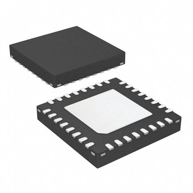
NQFP−32
5 SUFFIX
CASE 560AA
ORDERING INFORMATION
See detailed ordering and shipping information in the package
dimensions section on page 2 of this data sheet.
Field Programmable Node Addresses
Full Diagnostics and Status Information
Micro−Stepping Technology
Sensorless Step−Loss Detection
Peak Current Up to 800 mA
Fixed Frequency PWM Current−Control
Selectable PWM Frequency
Automatic Selection of Fast and Slow Decay Mode
No external Fly−back Diodes Required
14 V/24 V Compliant
Motion Qualification Mode (Note 1)
Protection
Overcurrent Protection
Undervoltage Management
Open−circuit Detection
High Temperature Warning and Management
Low Temperature Flag
EMI Compatibility
High Voltage Outputs with Slope Control
Controller with RAM and OTP Memory
Patents
Position Controller
Configurable Speeds and Acceleration
Input to Connect Optional Motion Switch
US 7,271,993
US 7,288,956
This is a Pb−Free Device
NCV Prefix for Automotive and Other Applications
I2C Interface
Bi−Directional 2−Wire Bus for Inter IC Control
Requiring Site and Control Changes
1. Not applicable for “Product Versions NCV70624DW010G, NCV70624DW010R2G”
Semiconductor Components Industries, LLC, 2009
September, 2009 − Rev. 5
1
Publication Order Number:
AMIS−30624/D
�AMIS−30624, NCV70624
APPLICATIONS
automation (HVAC, surveillance, satellite dish, renewable
energy systems). Suitable applications typically have
multiple axes or require mechatronic solutions with the
driver chip mounted directly on the motor.
The AMIS−30624/NCV70624 is ideally suited for small
positioning applications. Target markets include:
automotive (headlamp alignment, HVAC, idle control,
cruise control), industrial equipment (lighting, fluid control,
labeling, process control, XYZ tables, robots) and building
Table 1. ORDERING INFORMATION
Part No.
Peak Current
End Market/Version
Package*
Shipping†
AMIS30624C6244G
800 mA
SOIC−20
(Pb−Free)
Tube/Tray
AMIS30624C6244RG
800 mA
SOIC−20
(Pb−Free)
Tape & Reel
AMIS30624C6245G
800 mA
NQFP−32 (7 x 7 mm)
(Pb−Free)
Tube/Tray
AMIS30624C6245RG
800 mA
NQFP−32 (7 x 7 mm)
(Pb−Free)
Tape & Reel
NCV70624DW010G
800 mA
SOIC−20
(Pb−Free)
Tube/Tray
NCV70624DW010R2G
800 mA
SOIC−20
(Pb−Free)
Tape & Reel
Industrial
High Voltage Version
Automotive
High Temperature
Version
*For additional information on our Pb−Free strategy and soldering details, please download the ON Semiconductor Soldering and Mounting
Techniques Reference Manual, SOLDERRM/D.
†For information on tape and reel specifications, including part orientation and tape sizes, please refer to our Tape and Reel Packaging
Specification Brochure, BRD8011/D.
QUICK REFERENCE DATA
Table 2. ABSOLUTE MAXIMUM RATINGS
Parameter
Min
Max
Unit
VBB, VHW, VSWI
Supply voltage, hardwired address and SWI pins
−0.3
+40 (Note 2)
V
TJ
Junction temperature range (Note 3)
−50
+175
C
Tst
Storage temperature
−55
+160
C
Vesd (Note 4)
Human Body Model (HBM) Electrostatic discharge voltage on pins
−2
+2
kV
−200
+200
V
Machine Model (MM) Electrostatic discharge voltage on pins
Stresses exceeding Maximum Ratings may damage the device. Maximum Ratings are stress ratings only. Functional operation above the
Recommended Operating Conditions is not implied. Extended exposure to stresses above the Recommended Operating Conditions may affect
device reliability.
2. For limited time: VBB < 0.5 s, SWI and HW pins 15 seconds
SoftStop
HardUnder
HardStop
HardStop
HardStop
HardUnder
HardStop
HardUnder
VBB < UV2 and
t < 15 seconds
Stopped
= ‘1’
= ‘1’
Shutdown
HardStop;
= ‘1’
HardStop;
= ‘1’
Thermal
shutdown
[ = ‘1’]
Shutdown
SoftStop
SoftStop
Motion finished
n.a.
Stopped
Stopped
HardStop;
= ‘1’
Shutdown
Shutdown
Stopped;
=
Stopped;
=
n.a.
With the Following Color Code:
Command Ignored
NOTE:
Transition to Another State
Master is responsible for proper update (see Note 36)
See table notes on the following page.
http://onsemi.com
30
�AMIS−30624, NCV70624
31. = or or or
32. After power−on−reset, the state is entered.
33. A DualPosition sequence runs with a separate set of RAM registers. The parameters that are not specified in a DualPosition command are
loaded with the values stored in RAM at the moment the DualPosition sequence starts. is forced to ‘1’ during second motion.
at ‘0’ will be taken into account after the DualPosition sequence. A GetFullStatus1 command will return the default
parameters for and stored in RAM.
34. Shutdown state can be left only when and flags are reset.
35. Flags can be reset only after the master could read them via a GetFullStatus1 command, and provided the physical conditions allow
for it (normal temperature, correct battery voltage and no electrical or charge pump defect).
36. A SetMotorParam command sent while a motion is ongoing (state ) should not attempt to modify and values.
This can be done during a DualPosition sequence since this motion uses its own parameters, the new parameters will be taken into account
at the next SetPosition command.
37. = ‘1’ when register is loaded with a value different from the most negative value (i.e. different from 0x400 = “100 0000
0000”).
38. flag allows distinguishing whether state was entered after HardStop/SoftStop or not. is set to ‘1’ when leaving
state or and is reset during first clock edge occurring in state .
39. While in state , if there is a transition to state . This transition has the lowest priority,
meaning that , , etceteras are first evaluated for possible transitions.
40. If is active, then SetPosition and GotoSecurePosition commands are not ignored. can only be cleared
by a GetFullStatus1 command.
POR
Thermal Shutdown
Referencing
HardStop
Shutdown
HardStop
Thermal
ShutDown
SoftStop
HardStop
Dual Positioning Motion finished
Motion Finished
GotoSecPos
HardStop
Thermal Shutdown
Soft−stop
HardStop
SetPosition
Stopped
Motion Finished
GotoPos
GetFullStatus1
Motion Finished
Priorities
1
2
3
Vbb < UV2 or CPFAIL
4
Vbb < UV2 or CPFAIL
Vbb > UV1 and not CPFAIL
T > 15 sec
Figure 16. Simplified State Diagram
http://onsemi.com
31
HardUnder
ShutUnder
�AMIS−30624, NCV70624
Motordriver
Current Waveforms in the Coils
Figure 17 below illustrates the current fed to the motor coils by the motordriver in half−step mode.
Ix
Coil X
Iy
t
Coil Y
Figure 17. Current Waveforms in Motor Coils X and Y in Halfstep Mode
Whereas Figure 18 below shows the current fed to the coils in 1/16th micro stepping (1 electrical period).
Coil X
Iy
Ix
t
Coil Y
Figure 18. Current Waveforms in Motor Coils X and Y in 1/16th Micro−Step Mode
PWM Regulation
Table 22. PWM FREQUENCY SELECTION
In order to force a given current (determined by
or and the current position of the rotor) through
the motor coil while ensuring high energy transfer
efficiency, a regulation based on PWM principle is used. The
regulation loop performs a comparison of the sensed output
current to an internal reference, and features a digital
regulation generating the PWM signal that drives the output
switches. The zoom over one micro−step in the Figure 18
above shows how the PWM circuit performs this regulation.
To reduce the current ripple, a higher PWM frequency is
selectable. The RAM register PWMfreq is used for this.
PWMfreq
Applied PWM Frequency
0
22,8 kHz
1
45,6 kHz
PWM Jitter
To lower the power spectrum for the fundamental and
higher harmonics of the PWM frequency, jitter can be added
to the PWM clock. The RAM register is used
for this.
Table 23. PWM JITTER SELECTION
PWMJEn
http://onsemi.com
32
Status
0
Single PWM frequency
1
Added jitter to PWM frequency
�AMIS−30624, NCV70624
Motor Starting Phase
Motor Stopping Phase
At motion start, the currents in the coils are directly
switched from to with a new
sine/cosine ratio corresponding to the first half (or micro−)
step of the motion.
At the end of the deceleration phase, the currents are
maintained in the coils at their actual DC level (hence
keeping the sine/cosine ratio between coils) during the
stabilization time tstab (see AC Table). The currents are then
set to the hold values, respectively Ihold x sin(TagPos)
and Ihold x cos(TagPos), as illustrated below. A new
positioning order can then be executed.
Iy
Ix
t
Figure 19. Motor Stopping Phase
t stab
Charge Pump Monitoring
Motor Shutdown Mode
If the charge pump voltage is not sufficient for driving the
high side transistors (due to failure), an internal HardStop
command is issued. This is acknowledged to the master by
raising flag (available with command
GetFullStatus1).
In case this failure occurs while a motion is ongoing, the
flag is also raised.
A motor shutdown occurs when:
The chip temperature rises above the thermal shutdown
threshold Ttsd (see Thermal Shutdown Mode).
The battery voltage goes below UV2 for longer than 15
seconds (see Battery Voltage Management).
The charge pump voltage goes below the charge pump
comparator level for more than 15 seconds.
Flag = ‘1’, meaning an electrical problem is
detected on one or both coils, e.g. a short circuit.
Electrical Defect on Coils, Detection and Confirmation
The principle relies on the detection of a voltage drop on
at least one transistor of the H−bridge. Then the decision is
taken to open the transistors of the defective bridge.
This allows the detection the following short circuits:
External coil short circuit
Short between one terminal of the coil and Vbat or GND
A motor shutdown leads to the following:
H−bridges in high impedance mode.
The register is loaded with the ,
except in autarkic states.
The conditions to get out of a motor shutdown mode are:
Reception of a GetFullStatus1 command AND
The four above causes are no longer detected
One cannot detect an internal short in the motor.
Open circuits are detected by 100% PWM duty cycle
value during one electrical period with duration, determined
by Vmin.
This leads to H−bridges going in Ihold mode. Hence, the
circuit is ready to execute any positioning command.
Table 24. ELECTRICAL DEFECT DETECTION
Pins
Fault Mode
Yi or Xi
Short−circuit to GND
Yi or Xi
Short−circuit to Vbat
Yi or Xi
Open
Y1 and Y2
Short circuited
X1 and X2
Short circuited
Xi and Yi
Short circuited
http://onsemi.com
33
�AMIS−30624, NCV70624
This can be illustrated in the following sequence given as an application example. The master can check whether there is
a problem or not and decide which application strategy to adopt.
Table 25. Example of Possible Sequence used to Detect and Determine Cause of Motor Shutdown
Tj Tsd or
VBB UV2 (>15s) or
= ‘1’ or
= ‘1’ (>15s)
− The circuit is driven in motor shutdown
mode
− The application is not aware of this
SetPosition
frame
− The position set−point is
updated by the I2C Master
− Motor shutdown mode
no motion
− The application is still
unaware
Important: While in shutdown mode, since there is no hold
current in the coils, the mechanical load can cause a step loss,
which
indeed
cannot
be
flagged
by
the
AMIS−30624/NCV70624.
Note: The Priority Encoder is describing the management of
states and commands.
Warning: The application should limit the number of
consecutive GetFullStatus1 commands to try to get the
AMIS−30624/NCV70624 out of shutdown mode when this
proves to be unsuccessful, e.g. there is a permanent defect.
The reliability of the circuit could be altered since
GetFullStatus1 attempts to disable the protection of the
H−bridges.
GetFullStatus1 frame
GetFullStatus1 frame
...
− The application is aware
of a problem
− Possible confirmation of
the problem
− Reset or or or or
or by the application
− Possible new detection of over temperature or low
voltage or electrical problem Circuit sets or
or or or or
again at ‘1’
moving average and compares the value with two
independent threshold levels: Absolute threshold
(AbsThr[3:0]) and Delta threshold ().
Instructions for correct use of these two levels in
combination
with
three
additional
parameters
(, and )
are available in a dedicated Application Note “Robust
Motion Control with AMIS−3062x Stepper Motor Drivers”.
If the motor is accelerated by a pulling or propelling force
and the resulting back emf increases above the Delta
threshold (+DTHR), then is set. When the
motor is slowing down and the resulting back emf decreases
below the Delta threshold (−DTHR), then
is set. When the motor is blocked and the velocity is zero
after the acceleration phase, the back emf is low or zero.
When this value is below the Absolute threshold,
is set. The flag is the OR function
of OR OR
.
Motion Detection
Motion detection is based on the back emf generated
internally in the running motor. When the motor is blocked,
e.g. when it hits the end−stop, the velocity and as a result also
the generated back emf, is disturbed. The
AMIS−30624/NCV70624 senses the back emf, calculates a
Velocity
Vbemf
+DTHR
Vmax
Motor speed
Vmin
Vbemf
−DTHR
t
t
Vbemf
Vbemf
DeltaStallHi
VABSTH
Back emf
t
t
DeltaStallLo
AbsStall
t
t
Figure 20. Triggering of the Stall Flags in Function of Measured Backemf and the Set Threshold Levels
http://onsemi.com
34
�AMIS−30624, NCV70624
Table 26. TRUTH TABLE
Condition
Vbemf < Average − DelThr
1
0
0
1
Vbemf > Average + DelThr
0
1
0
1
Vbemf < AbsThr
0
0
1
1
By design, the motion will only be detected when the
motor is running at the maximum velocity, not during
acceleration or deceleration.
If the motor is positioning when Stall is detected, an
(internal) hardstop of the motor is generated and the
and flags are set. These flags can
only be reset by sending a GetFullStatus1 command.
If Stall appears during DualPosition then the first phase is
cancelled (via internal hardstop) and after timeout Tstab (see
AC table) the second phase at Vmin starts.
When the flag is set the position controller will
generate an internal HardStop. As a consequence also the
flag will be set. The position in the internal
counter will be copied to the register. All flags
can be read out with the GetFullStatus1 command.
Table 27.
ABSOLUTE AND DELTA THRESHOLD SETTINGS
AbsThr
Index
AbsThr
Level (V) (*)
DelThr
Index
DelThr
Level (V) (*)
0
Disable
0
Disable
1
0.5
1
0.25
2
1.0
2
0.50
3
1.5
3
0.75
4
2.0
4
1.00
5
2.5
5
1.25
6
3.0
6
1.50
7
3.5
7
1.75
8
4.0
8
2.00
Important Remark (limited to motion detection flags /
parameters):
Using GetFullStatus1 will read AND clear the
following flags: , , ,
and . New positioning is
possible and the register will be further updated.
Motion detection is disabled when the RAM registers
and are zero. Both
levels can be programmed using the I2C command
SetStallParam in the registers and
.
Also
the
OTP
register
and can be set
using the I2C command SetOTPParam. These values are
copied in the RAM registers during power on reset.
9
4.5
9
2.25
A
5.0
A
2.50
B
5.5
B
2.75
C
6.0
C
3.00
D
6.5
D
3.25
E
7.0
E
3.50
F
7.5
F
3.75
(*) Not tested in production. Values are approximations.
MinSamples
is a programmable delay timer.
After the zero crossing is detected, the delay counter is
started. After the delay time−out (tdelay) the back−emf
sample is taken. For more information please refer to the
Application Note “Robust Motion Control with
AMIS−3062x Stepper Motor Drivers”.
Table 28. BACK EMF SAMPLE DELAY TIME
Index
MinSamples[2:0]
tDELAY (ms)
0
000
87
1
001
130
2
010
174
3
011
217
4
100
261
5
101
304
6
110
348
7
111
391
http://onsemi.com
35
�AMIS−30624, NCV70624
FS2StallEn
high as 100%. This indicates that the supply is too low to
generate the required torque and might also result in
erroneously triggering the stall detection. The bit
enables stall detection when duty cycle is
100%. For more information please refer to the Application
Note “Robust Motion Control with AMIS−3062x Stepper
Motor Drivers”.
If or 0 (i.e. motion detection
is enabled), then stall detection will be activated AFTER the
acceleration ramp + an additional number of full−steps,
according to the following table:
Table 29. ACTIVATION DELAY OF MOTION
DETECTION
Index
FS2StallEn[2:0]
Delay (Full Steps)
0
000
0
1
001
1
2
010
2
3
011
3
4
100
4
5
101
5
6
110
6
7
111
7
Motion Qualification Mode (*)
This mode is useful to debug motion parameters and to
verify the stability of stepper motor systems. The motion
qualification mode is entered by means of the I2C command
TestBemf. The SWI pin will be converted into an
analogue output on which the Back EMF integrator output
can be measured. Once activated, it can only be stopped after
a POR. During the Back emf observation, reading of the
SWI state is internally forbidden.
(*) Note: Not applicable for product versions
NCV70624DW010G, NCV70624DW010R2G.
More information is available in the Application Note
“Robust Motion Control with AMIS−3062x Stepper Motor
Drivers”.
DC100StEn
When a motor with large bemf is operated at high speed
and low supply voltage, then the PWM duty cycle can be as
http://onsemi.com
36
�AMIS−30624, NCV70624
I2C BUS DESCRIPTION
General Description
AMIS−30624/NCV70624 uses a simple bi−directional
2−wire bus for efficient inter−ic control. This bus is called
the Inter IC or I2C−bus.
Features include:
Only two bus lines are required; a serial data line
(SDA) and a serial clock line (SCK).
Each device connected to the bus is software
addressable by a unique address and simple
master/slave relationships exists at all times; master can
operate as master−transmitter or as master receiver.
Serial, 8−bit oriented, bi−directional data transfers can
be made up to 400 kb/s.
On−chip filtering rejects spikes on the bus data line to
preserve data integrity.
No need to design bus interfaces because I2C−bus
interface is already integrated on−chip.
IC’s can be added to or removed from a system without
affecting any other circuits on the bus.
Concept
The I2C−bus consists of two wires, serial data (SDA) and
serial clock (SCK), carrying information between the
devices connected on the bus. Each device connected to the
bus is recognized by a unique address and operates as either
a transmitter or receiver, depending on the function of the
device. AMIS−30624/NCV70624 can both receive and
transmit data. In addition to transmitters and receivers,
devices can also be considered as masters or slaves when
performing data transfers. AMIS−30624/NCV70624 is a
slave device. See Table 31.
Table 30. DEFINITION OF I2C–BUS TERMINOLOGY
Term
Description
Transmitter
The device which sends data on the bus
Receiver
The device which receives data from the bus
Master
The device which initiates a transfer, generates clock signals and terminates a transfer
Slave
The devices addressed by a master
Synchronization
Procedure to synchronizer the clock signals of two or more devices
Micro−
controller
Motordriver_2
Motordriver_4
AMIS−30624,
NCV70624
AMIS−30624,
NCV70624
SDA
SCL
Motordriver_1
Motordriver_3
AMIS−30624,
NCV70624
AMIS−30624,
NCV70624
Figure 21. Example of an I2C−bus Configuration Using One Microcontroller and Four Slaves
Figure 21
highlights
the
master−slave
and
receiver−transmitter relationships to be found on the
I2C−bus. It should be noted that these relationships are not
permanent but only depend on the direction of data transfer
at that time. The transfer of data would proceed as follows:
1. Suppose the microcontroller wants to send
information to motordriver_1:
Microcontroller (master) addresses
motordriver_1 (slave)
Microcontroller (master−transmitter) sends data
to motordriver_1 (slave−receiver)
Microcontroller terminates the transfer
2. If the microcontroller wants to receive information
from motordriver_2:
Microcontroller (master) addresses
motordriver_2 (slave)
Microcontroller (master−receiver) receives data
from motordriver_2 (slave−transmitter)
Microcontroller terminates the transfer
Even in this case the master generates the timing and
terminates the transfer.
Generation of the signals on the I2C−bus is always the
responsibility of the master device. It generates its own
clock signal when transferring data on the bus. Bus clock
signals from a master can only be altered when they are
stretched by a slow slave device holding−down the clock
line.
http://onsemi.com
37
�AMIS−30624, NCV70624
General Characteristics
+5 V
Rp
Rp
Serial Data Line
Serial Clock Line
SCK
SDA
2
Clock IN
SCL
1
Data IN
Clock OUT
SDA
Clock IN
Data OUT
Data IN
Clock OUT
AMIS−30624,
NCV70624
Data OUT
MASTER
Figure 22. Connection of a Device to the I2C−bus
START and STOP Conditions
Both SDA and SCK are bi−directional lines connected to
a positive supply voltage via a pull−up resistor (see
Figure 22). When the bus is free both lines are HIGH. The
output stages of the devices connected to the bus must have
an open drain to perform the wired−AND function. Data on
the I2C−bus can be transferred up to 400 kb/s in fast mode.
The number of interfaces connected to the bus is dependent
on the maximum bus capacitance limit (See CB in Table 6)
and the available number of addresses.
Within the procedure of the I2C−bus, unique situations
arise, which are defined as START (S) and STOP (P)
conditions (See Figure 24).
A HIGH to LOW transition on the SDA line while SCK
is HIGH is one such unique case. This situation indicates a
START condition. LOW to HIGH transition on the SDA line
while SCK is HIGH defines a STOP condition.
START and STOP conditions are always generated by the
master. The bus is considered to be busy after the START
condition. The bus is considered to be free again a certain
time after the STOP condition. The bus free situation is
specified as tBUF in Table 6.
The bus stays busy if a repeated START (Sr) is generated
instead of a STOP condition. In this respect, the START (S)
and repeated START (Sr) conditions are functionally
identical (See Figure 25). The symbol S will be used to
represent START and repeated START, unless otherwise
noted.
Bit Transfer
The levels for logic ‘0’ (LOW) and ‘1’ (HIGH) are not
fixed in the I2C standard but dependent on the used VDD
level. Using AMIS−30624/NCV70624, the levels are
specified in Table 5. One clock pulse is generated for each
data bit transferred.
Data Validity
The data on the SDA line must be stable during the HIGH
period of the clock. The HIGH or LOW state of the data line
can only change when the clock signal on the SCL line is
LOW (See Figure 23).
START
STOP
SDA
SDA
SCK
SCK
Data line stable
−> Data valid
Change of
data allowed
START
condition
Figure 23. Bit Transfer on the I2C−bus
STOP
condition
Figure 24. START and STOP Conditions
http://onsemi.com
38
�AMIS−30624, NCV70624
Transferring Data
with the most significant bit (MSB) first (See Figure 25). If
a slave can’t receive or transmit another complete byte of
data, it can hold the clock line SCK LOW to force the master
into a wait state. Data transfer then continues when the slave
is ready for another byte of data and releases clock line SCK.
Byte Format
Every byte put on the SDA line must be 8−bits long. The
number of bytes that can be transmitted per transfer to
AMIS−30624/NCV70624 is restricted to eight. Each byte
has to be followed by an acknowledge bit. Data is transferred
START
STOP
SDA
MSB
Acknowledgement
signal from slave
SCK
1
7
2
8
Clock line held
low by slave
9
1
2
3−8
9
ACK
START
condition
STOP
condition
Aknowledge related
clock puse from master
Figure 25. Data Transfer on the I2C−bus
Acknowledge
If AMIS−30624/NCV60624 as slave−receiver does
acknowledge the slave address but later in the transfer
cannot receive any more data bytes, this is indicated by
generating a not−acknowledge on the first byte to follow.
The master generates than a STOP or a repeated START
condition.
If a master−receiver is involved in the transfer, it must
signal the end of data to the slave−transmitter by not
generating an acknowledge on the last byte that was clocked
out of the slave. AMIS−30624/NCV70624 as
slave−transmitter shall release the data line to allow the
master to generate STOP or repeated START condition.
Data transfer with acknowledge is obligatory. The
acknowledge−related clock pulse is generated by the master.
The transmitter releases the SDA line (HIGH) during the
acknowledge clock pulse. The receiver must pull down the
SDA line during the acknowledge clock pulse so that it
remains stable LOW during the HIGH period of this clock
pulse (see Figure 26). Of course, set−up and hold times must
also taken into account (see Table 6). When
AMIS−30624/NCV60624 doesn’t acknowledge the slave
address, the data line will be left HIGH. The master can than
generate either a STOP condition to abort the transfer, or a
repeated START condition to start a new transfer.
START
Master releases the Data line
SDA by master
transmitter
MSB
Not acknowledged
SDA by slave
receiver
Acknowledged
SCK from
master
1
START
condition
8
2
Slave pulls data line
low if Acknowledged
9
Aknowledge related
clock puse from master
Figure 26. Acknowledge on the I2C−bus
http://onsemi.com
39
�AMIS−30624, NCV70624
Clock Generation
address is 7−bit long followed by an eighth bit which is a data
direction bit (R/W) − a ‘zero’ indicates a transmission
(WRITE), a ‘one’ indicates a request for data (READ). A
data transfer is always terminated by a STOP condition (P)
generated by the master.
The master generates the clock on the SCK line to transfer
messages on the I2C−bus. Data is only valid during the
HIGH period of the clock.
Data Formats with 7−bit Addresses
Data transfers follow the format shown in Figure 27. After
the START condition (S), a slave address is sent. This
START
STOP
SDA
SCK
1−7
START
condition
ADDRESS
8
9
R/W
ACK
8
1−7
9
DATA
1−7
ACK
9
8
DATA
ACK
STOP
condition
Figure 27. A Complete Data Transfer
However, if a master still wishes to communicate on the
bus, it can generate a repeated START (Sr) and address
another slave without first generating a STOP condition.
Various combinations of read/write formats are then
possible within such a transfer.
Data Transfer Formats
Writing Data to AMIS−30624/NCV70624
When writing to AMIS−30624/NCV70624, the
master−transmitter transmits to slave−receiver and the
transfer direction is not changed. A complete transmission
consists of:
Start condition
S
Slave Address
R/W
A
Data
AMIS−30624 to Master
A
Data
A
P
N bytes + Acknowledge
”0” = WRITE
Master to AMIS−30624
The slave address (7−bit)
Read/Write bit (‘0’ = write)
Acknowledge bit
Any further data bytes are followed by an
acknowledge bit. The acknowledge bit is used to
signal a correct reception of the data to the
transmitter. In this case the
AMIS−30624/NCV70624 pulls the SDA line to ‘0’.
The AMIS−30624/NCV70624 reads the incoming
data at SDA on every rising edge of the SCK signal
Stop condition to finish the transmission
S = Start condition
P = Stop condition
A = Acknowledge (SDA = LOW)
A = No Acknowledge (SDA = HIGH)
Figure 28. Master Writing Data to AMIS−30624/NCV70624
1. The first transmission consists of two bytes of
data:
The first byte contains the slave address and the
write bit.
The second byte contains the address of an
internal register in the
AMIS−30624/NCV70624. This internal
register address is stored in the circuit RAM.
Some commands for the AMIS−30624/NCV70624 are
supporting eight bytes of data, other commands are
transmitting two bytes of data. See Table 31.
Reading Data to AMIS−30624/NCV70624
When reading data from AMIS−30624/NCV70624 two
transmissions are needed:
http://onsemi.com
40
�AMIS−30624, NCV70624
S
Slave Address
R/W
A
Internal Address
A
P
”0” = WRITE
Figure 29. Master Reading Data from AMIS−30624/NCV70624: First Transmission is Addressing
pulling SDA LOW. The last byte is not
acknowledged by the master and therefore the
slave knows the end of transmission.
2. The second transmission consists of the slave
address and the read bit. Then the master can read
the data bits on the SDA line on every rising edge
of signal SCK. After each byte of data the master
has to acknowledge correct data reception by
S
Slave Address
R/W
A
Data
Data
A
P
N bytes + Acknowledge
”0” = WRITE
Master to AMIS−30624
A
S = Start condition
P = Stop condition
A = Acknowledge (SDA = LOW)
A = No Acknowledge (SDA = HIGH)
AMIS−30624 to Master
Figure 30. Master Reading Data from AMIS−30624/NCV70624: Second Transmission is Reading Data
Notes:
1. Each byte is followed by an acknowledgment bit as indicated by the A or A in the sequence.
2. I2C−bus compatible devices must reset their bus logic on receipt of a START condition such that they all anticipate the sending of a
slave address, even if these START conditions are not positioned according to the proper format.
3. A START condition immediately followed by a STOP condition (void message) is an illegal format.
7−bit Addressing
The addressing procedure for the I2C−bus is such that the
first byte after the START condition usually determines
which slave will be selected by the master. The exception is
the general call address which can call all devices. When this
address is used all devices should respond with an
acknowledge. The second byte of the general call address
then defines the action to be taken.
AMIS−30624/NCV70624 is provided with a physical
address in order to discriminate this circuit from other
circuits on the I2C bus. This address is coded on seven bits
(two bits being internally hardwired to ‘1’), yielding the
theoretical possibility of 32 different circuits on the same
bus. It is a combination of four OTP memory bits (OTP
Memory Structure OPEN) and of the externally hardwired
address bits (pin HW). HW must either be connected to
ground or to Vbat. When HW is not connected and is left
floating, correct functionality of the positioner is not
guaranteed. The motor will be driven to the programmed
secure position (See Hardwired Address – OPEN).
Definition of Bits in the First Byte
The first seven bits of the first byte make up the slave
address. The eighth bit is the least significant bit (LSB). It
determines the direction of the message. If the LSB is a
“zero” it means that the master will write information to a
selected slave. A “one” in this position means that the master
will read information from the slave. When an address is
sent, each device in a system compares the first seven bits
after the START condition with its address. If they match,
the device considers itself addressed by the master as a
slave−receiver or slave−transmitter, depending on the R/W
bit.
MSB
LSB
MSB
1
1
PA3 PA2 PA1 PA0 HW R/W
OTP memory
Hardwired Address Bit
Figure 32. First Byte after START Procedure
LSB
General Call Address
R/W
The AMIS−30624/NCV70624 supports also a “general
call” address “000 0000”, which can address all devices.
When this address is used all devices should respond with an
acknowledge. The second byte of the general call address
then defines the action to be taken.
SLAVE ADDRESS
Figure 31. First Byte after START Procedure
http://onsemi.com
41
�AMIS−30624, NCV70624
I2C APPLICATION COMMANDS
Introduction
Communications between the AMIS−30624/NCV70624
and a 2−wire serial bus interface master takes place via a
large set of commands.
Reading commands are used to:
Get actual status information, e.g. error flags
Get actual position of the stepper motor
Verify the right programming and configuration of
the AMIS−30624/NCV70624.
Writing commands are used to:
Program the OTP memory
Configure the positioner with motion parameters
(max/min speed, acceleration, stepping mode, etc.)
Provide target positions to the Stepper motor
The I2C−bus master will have to use commands to manage
the different application tasks the AMIS−30624/NCV70624
can feature. The commands summary is given in Table 31.
Commands Table
Table 31. I2C COMMANDS WITH CORRESPONDING ROM POINTER
Command Byte
Command Mnemonic
Function
Binary
Hexadecimal
GetFullStatus1
Returns complete status of the chip
“1000 0001”
0x81
GetFullStatus2
Returns actual, target and secure position
“1111 1100”
0xFC
GetOTPParam
Returns OTP parameter
“1000 0010”
0x82
GotoSecurePosition
Drives motor to secure position
“1000 0100”
0x84
HardStop
Immediate full stop
“1000 0101”
0x85
ResetPosition
Sets actual position to zero
“1000 0110”
0x86
ResetToDefault
Overwrites the chip RAM with OTP contents
“1000 0111”
0x87
SetDualPosition
Drives the motor to two different positions with
different speed
“1000 1000”
0x88
SetMotorParam
Sets motor parameter
“1000 1001”
0x89
SetOTP
Zaps the OTP memory
“1001 0000”
0x90
SetPosition
Programs a target and secure position
“1000 1011”
0x8B
SetStallParam
Sets stall parameters
“1001 0110”
0x96
SoftStop
Motor stopping with deceleration phase
“1000 1111”
0x8F
Runvelocity
Drives motor continuously
“1001 0111”
0x97
TestBemf
Outputs Bemf voltage on pin SWI
“1001 1111”
0x9F
These commands are described hereafter, with their
corresponding I2C frames. Refer to Data Transfer Formats
for more details. A color coding is used to distinguish
between master and slave parts within the frames. An
example is shown below.
Light Gray: Master Data
White: Slave Response
Figure 33. Color Code Used in the Definition of I2C Frames
http://onsemi.com
42
�AMIS−30624, NCV70624
Application Commands
Note: A GetFullStatus1 command will attempt to
reset flags , , , ,
, , , , and
.
GetFullStatus1
This command is provided to the circuit by the master to
get a complete status of the circuit and of the stepper motor.
Refer to Tables 19 and 20 to see the meaning of the
parameters sent back to the I2C master.
GetFullStatus1 corresponds to the following I2C command frame:
Table 32. GetFullStatus1 COMMAND FRAME
Structure
Content
Bit 7
Bit 6
Bit 5
Bit 4
Bit 3
Bit 2
Bit 1
Bit 0
0
Address
1
1
OTP3
OTP2
OTP1
OTP0
HW
0
1
Command
1
0
0
0
0
0
0
1
Byte
Table 33. GetFullStatus1 RESPONSE FRAME
Structure
Byte
Content
Bit 7
Bit 6
Bit 5
Bit 4
Bit 3
Bit 2
Bit 1
Bit 0
0
Address
1
1
OTP3
OTP2
OTP1
OTP0
HW
1
1
Address
1
1
1
OTP3
OTP2
OTP1
OTP0
HW
2
Data 1
Irun[3:0]
Ihold[3:0]
3
Data 2
Vmax[3:0]
Vmin[3:0]
4
Data 3
AccShape
5
Data 4
VddReset
6
Data 5
7
Data 6
8
Data 7
Where:
OTP(n)
HW
Irun[3:0]
Ihold[3:0]
Vmax[3:0]
Vmin[3:0]
AccShape
StepMode[1:0]
Shaft
Acc[3:0]
VddReset
StepLoss
StepMode[1:0]
StepLoss
ElDef
Motion[2:0]
1
1
Shaft
UV2
TSD
TW
ESW
OVC1
OVC2
Stall
CPFail
1
1
1
1
1
1
AbsThr[3:0]
OTP address bits PA[3:0]
Hardwired address bit
Operating current in the motor coil
Standstill current in the motor coil
Maximum velocity
Minimum velocity
Enables motion without acceleration
Step mode definition
Direction of movement
Acceleration form minimum to
maximum velocity
Reset of digital supply
Step loss occurred
ElDef
UV2
TSD
TW
Tinfo[1:0]
Motion[2:0]
ESW
OVC1
OVC2
Stall
CPFail
AbsThr[3:0]
DelThr[3:0]
http://onsemi.com
43
Acc[3:0]
Tinfo[1:0]
DelThr[3:0]
Electrical defect
Battery under voltage detected
Thermal shutdown
Thermal warning
Temperature Info
Motion status
External switch status
Over current in X−coil detected
Over current in Y−coil detected
Stall detected
Charge pump failure
Stall detection absolute threshold
Stall detection delta threshold
�AMIS−30624, NCV70624
GetFullStatus2
stepping mode the LSBs of ActPos[15:0] and
TagPos[15:0] may have no meaning and should be
assumed to be ‘0’. This command also gives additional
information concerning stall detection. Refer to Tables 19
and 20 to see the meaning of the parameters sent back to the
I2C master.
This command is provided to the circuit by the master to
get the actual, target and secure position of the stepper
motor. Both the actual and target position are returned in
signed two’s complement 16−bit format. Secure position is
coded in 10−bit format. According to the programmed
GetFullStatus2 corresponds to the following I2C command frame:
Table 34. GetFullStatus2 COMMAND FRAME
Structure
Content
Bit 7
Bit 6
Bit 5
Bit 4
Bit 3
Bit 2
Bit 1
Bit 0
0
Address
1
1
OTP3
OTP2
OTP1
OTP0
HW
0
1
Command
1
1
1
1
1
1
0
0
Byte
Table 35. GetFullStatus2 RESPONSE FRAME
Structure
Byte
Content
Bit 7
Bit 6
Bit 5
Bit 4
Bit 3
Bit 2
Bit 1
Bit 0
0
Address
1
1
OTP3
OTP2
OTP1
OTP0
HW
1
1
Address
1
1
1
OTP3
OTP2
OTP1
OTP0
HW
2
Data 1
ActPos[15:8]
3
Data 2
ActPos[7:0]
4
Data 3
TagPos[15:8]
5
Data 4
TagPos[7:0]
6
Data 5
SecPos[7:0]
7
Data 6
8
Data 7
Where:
OTP(n)
HW
ActPos[15:0]
TagPos[15:0]
SecPos[10:0]
FS2StallEn[2:0]
DC100
FS2StallEn[2:0]
AbsStall
DelStallLo
1
DelStallHi
DC100
MinSamples[2:0]
AbsStall
SecPos[10:8]
DC100StEn
PWMJEn
Stall detected because the absolute
threshold is not reached
DelStallLo
Stall detected because the delta threshold
is under crossed
DelStallHi:
Stall detected because the delta threshold
is crossed
MinSamples[2:0] Back−emf sampling delay time
DC100StEn
Enables the switch off of stall detection
when DC100 = 1
PWMJEn
PWM jitter enable
OTP address bits PA[3:0]
Hardwired address bit
Actual position
Target position
Secure position
Number of full steps after stall detection
is enabled
Flag indicating PWM is at 100 percent
duty cycle
http://onsemi.com
44
�AMIS−30624, NCV70624
GetOTPParam
This command is provided to the circuit by the I2C master
to read the content of the OTP memory. More information
can be found in OTP Memory Structure corresponds to the
following I2C command frame:.
GetOTPParam
Table 36. GetOTPParam COMMAND FRAME
Structure
Byte
Content
Bit 7
Bit 6
Bit 5
Bit 4
Bit 3
Bit 2
Bit 1
Bit 0
0
Address
1
1
OTP3
OTP2
OTP1
OTP0
HW
0
1
Command
1
0
0
0
0
0
1
0
Bit 4
Bit 3
Bit 2
Bit 1
Bit 0
OTP2
OTP1
OTP0
HW
1
Table 37. GetOTPParam RESPONSE FRAME
Structure
Content
Bit 7
Bit 6
Bit 5
0
Address
1
1
OTP3
1
OTP byte 0
OTP byte @0x00
2
OTP byte 1
OTP byte @0x01
3
OTP byte 2
OTP byte @0x02
4
OTP byte 3
OTP byte @0x03
5
OTP byte 4
OTP byte @0x04
6
OTP byte 5
OTP byte @0x05
7
OTP byte 6
OTP byte @0x06
8
OTP byte 7
OTP byte @0x07
Byte
the following I2C command frame: description for more
details. The priority encoder table also acknowledges the
cases where a GotoSecurePosition command will be
ignored.
GotoSecurePosition
This command is provided by the I2C master to one or all
the stepper motors to move to the secure position
SecPos[10:0]. See the priority encoder corresponds to
GotoSecurePosition
Table 38. GotoSecurePosition COMMAND FRAME
Structure
Byte
Content
Bit 7
Bit 6
Bit 5
Bit 4
Bit 3
Bit 2
Bit 1
Bit 0
0
Address
1
1
OTP3
OTP2
OTP1
OTP0
HW
0
1
Command
1
0
0
0
0
1
0
0
http://onsemi.com
45
�AMIS−30624, NCV70624
HardStop
master at the next GetStatus1 command that steps may
have been lost. Once the motor is stopped, ActPos register
is copied into TagPos register to ensure keeping the stop
position. The I2C master for some safety reasons can also
issue a HardStop command.
This command will be internally triggered when an
electrical problem is detected in one or both coils, leading to
shutdown mode. If this occurs while the motor is moving,
the flag is raised to allow warning of the I2C
HardStop corresponds to the following I2C command frame:
Table 39. HardStop COMMAND FRAME
Structure
Byte
Content
Bit 7
Bit 6
Bit 5
Bit 4
Bit 3
Bit 2
Bit 1
Bit 0
0
Address
1
1
OTP3
OTP2
OTP1
OTP0
HW
0
1
Command
1
0
0
0
0
1
0
1
ResetPosition
This command is provided to the circuit by the I2C master
to reset ActPos and TagPos registers to zero. This can be
helpful to prepare for instance a relative positioning.
ResetPosition corresponds to the following I2C command frame:
Table 40. ResetPosition COMMAND FRAME
Structure
Byte
Content
Bit 7
Bit 6
Bit 5
Bit 4
Bit 3
Bit 2
Bit 1
Bit 0
0
Address
1
1
OTP3
OTP2
OTP1
OTP0
HW
0
1
Command
1
0
0
0
0
1
1
0
Note: ActPos and TagPos are not modified by a
ResetToDefault command.
Important: Care should be taken not to send a
ResetToDefault command while a motion is ongoing,
since this could modify the motion parameters in a way
forbidden by the position controller.
ResetToDefault
This command is provided to the circuit by the I2C master
in order to reset the whole slave node into the initial state.
ResetToDefault will, for instance, overwrite the RAM
with the reset state of the registers parameters (see Table 19).
This is another way for the I2C master to initialize a slave
node in case of emergency, or simply to refresh the RAM
content.
ResetToDefault corresponds to the following I2C command frame:
Table 41. ResetToDefault COMMAND FRAME
Structure
Byte
Content
Bit 7
Bit 6
Bit 5
Bit 4
Bit 3
Bit 2
Bit 1
Bit 0
0
Address
1
1
OTP3
OTP2
OTP1
OTP0
HW
0
1
Command
1
0
0
0
0
1
1
1
RunVelocity
This command is provided to the circuit by the I2C master
in order to put the motor in continuous motion state.
RunVelocity corresponds to the following I2C command frame:
Table 42. RunVelocity COMMAND FRAME
Structure
Content
Bit 7
Bit 6
Bit 5
Bit 4
Bit 3
Bit 2
Bit 1
Bit 0
0
Address
1
1
OTP3
OTP2
OTP1
OTP0
HW
0
1
Command
1
0
0
1
0
1
1
1
Byte
http://onsemi.com
46
�AMIS−30624, NCV70624
SetDualPosition
command is issued, the circuit will enter in deadlock state.
Therefore, the application should check the actual position
by a GetFullStatus2 corresponds to the following I2C
command frame command prior to starting a dual
positioning. Another solution may consist of programming
a value out of the stepper motor range for Pos1[15:0].
For the same reason Pos2[15:0] should not be equal to
Pos1[15:0].
This command is provided to the circuit by the I2C master
in order to perform a positioning of the motor using two
different velocities. See Section Dual Positioning.
Note: This sequence cannot be interrupted by another
positioning command.
Important: If for some reason ActPos equals
Pos1[15:0] at the moment the SetDualPosition
SetDualPosition
Table 43. SetDualPosition COMMAND FRAME
Structure
Content
Bit 7
Bit 6
Bit 5
Bit 4
Bit 3
Bit 2
Bit 1
Bit 0
0
Address
1
1
OTP3
OTP2
OTP1
OTP0
HW
0
1
Command
1
0
0
0
1
0
0
0
2
Data 1
1
1
1
1
1
1
1
1
3
Data 2
1
1
1
1
1
1
1
1
4
Data 3
5
Data 4
6
Data 5
Pos1[7:0]
7
Data 6
Pos2[15:8]
8
Data 7
Pos2[7:0]
Byte
Where:
Vmax[3:0]
Vmin[3:0]
Vmax[3:0]
Vmin[3:0]
Pos1[15:8]
Max. velocity for first motion
Min. velocity for first motion and
velocity for the second motion
Pos1[15:0]
Pos2[15:0]
First position to be reached during the
first motion
Relative position of the second motion
SetStallParam
This command sets the motion detection parameters and
the related stepper motor parameters, such as the minimum
and maximum velocity, the run− and hold current,
acceleration and step−mode. See Motion Detection
corresponds to the following I2C command frame for the
meaning of these parameters.
SetStallParam
Table 44. SetStallParam COMMAND FRAME
Structure
Byte
Content
Bit 7
Bit 6
Bit 5
Bit 4
Bit 3
Bit 2
Bit 1
Bit 0
0
Address
1
1
OTP3
OTP2
OTP1
OTP0
HW
0
1
Command
1
0
0
1
0
1
1
0
2
Data 1
1
1
1
1
1
1
1
1
3
Data 2
1
1
1
1
1
1
1
1
4
Data 3
Irun[3:0]
Ihold[3:0]
5
Data 4
Vmax[3:0]
Vmin[3:0]
6
Data 5
7
Data 6
8
Data 7
MinSamples[2:0]
Shaft
AbsThr[3:0]
FS2StallEn[2:0]
DelThr[3:0]
AccSha
pe
http://onsemi.com
47
Acc[3:0]
StepMode[1:0]
DC100S
tEn
PWMJE
n
�AMIS−30624, NCV70624
SetMotorParam
This command is provided to the circuit by the I2C master
to set the values for the stepper motor parameters (listed
below) in RAM. Refer to Table 19 to see the meaning of the
parameters sent by the I2C master.
Important: If a SetMotorParam occurs while a motion
is ongoing, it will modify at once the motion parameters (see
Position Controller corresponds to the following I2C
command frame:). Therefore the application should not
change parameters other than Vmax while a motion is
running, otherwise correct positioning cannot be
guaranteed.
SetMotorParam
Table 45. SetMotorParam COMMAND FRAME
Structure
Byte
Content
Bit 7
Bit 6
Bit 5
Bit 4
Bit 3
Bit 2
Bit 1
Bit 0
0
Address
1
1
OTP3
OTP2
OTP1
OTP0
HW
0
1
Command
1
0
0
0
1
0
0
1
2
Data 1
1
1
1
1
1
1
1
1
3
Data 2
1
1
1
1
1
1
1
1
4
Data 3
Irun[3:0]
Ihold[3:0]
5
Data 4
Vmax[3:0]
Vmin[3:0]
6
Data 5
7
Data 6
8
Data 7
SecPos[10:8]
Shaft
Acc[3:0]
SecPos[7:0]
1
PWMfre
q
1
AccSha
pe
StepMode[1:0]
1
PWMJE
n
SetOTPParam
This command is provided to the circuit by the I2C master
to program and zap the OTP data D[7:0] in OTP address
OTPA[2:0].
Important: This command must be sent under a specific
VBB voltage value. See parameter VBBOTP in Table 5. This
is a mandatory condition to ensure reliable zapping.
SetOTPParam corresponds to the following I2C command frame:
Table 46. SetOTPParam COMMAND FRAME
Structure
Byte
Content
Bit 7
0
Address
1
1
OTP3
OTP2
OTP1
OTP0
HW
0
1
Command
1
0
0
1
0
0
0
0
2
Data 1
1
1
1
1
1
1
1
1
3
Data 2
1
1
1
1
1
1
1
1
4
Data 3
1
1
1
1
5
Data 4
Where:
OTPA[2:0]:
D[7:0]:
Bit 6
Bit 5
Bit 4
Bit 3
Bit 2
Bit 1
Bit 0
1
D[7:0]
OTP address
Corresponding OTP data
http://onsemi.com
48
OTPA[2:0]
�AMIS−30624, NCV70624
SetPosition
This command is provided to the circuit by the I2C master
to drive the motor to a given absolute position. See
Positioning (see Priority Encoder) for more details. The
priority encoder table acknowledges the cases where a
SetPosition command will be ignored.
SetPosition corresponds to the following I2C command frame:
Table 47. SetPosition COMMAND FRAME
Structure
Byte
Content
Bit 7
Bit 6
Bit 5
Bit 4
Bit 3
Bit 2
Bit 1
Bit 0
0
Address
1
1
OTP3
OTP2
OTP1
OTP0
HW
0
1
Command
1
0
0
0
1
0
1
1
2
Data 1
1
1
1
1
1
1
1
1
3
Data 2
1
1
1
1
1
1
1
1
4
Data 3
Pos[15:8]
5
Data 4
Pos[7:0]
Where:
Pos [15:0]
Signed 16−bit position set−point for motor.
SoftStop
command frame:) followed by a stop, regardless of the
position reached. Once the motor is stopped, TagPos
register is overwritten with value in ActPos register to
ensure keeping the stop position. The I2C Master for some
safety reasons can also issue a SoftStop command.
This command will be internally triggered when the chip
temperature rises above the thermal shutdown threshold (see
Table 5 and the Temperature Management Section). It
provokes an immediate deceleration to Vmin (see
Minimum Velocity corresponds to the following I2C
SoftStop
Table 48. SoftStop COMMAND FRAME
Structure
Byte
Content
Bit 7
Bit 6
Bit 5
Bit 4
Bit 3
Bit 2
Bit 1
Bit 0
0
Address
1
1
OTP3
OTP2
OTP1
OTP0
HW
0
1
Command
1
0
0
0
1
1
1
1
TestBemf
This command is provided to the circuit by the I2C master
in order to output the Bemf integrator output to the SWI
output of the chip. Once activated, it can be stopped only
after POR. During the Bemf observation, reading of the SWI
state is internally forbidden.
TestBemf corresponds to the following I2C command frame:
Table 49. TestBemf COMMAND FRAME
Structure
Byte
Content
Bit 7
Bit 6
Bit 5
Bit 4
Bit 3
Bit 2
Bit 1
Bit 0
0
Address
1
1
OTP3
OTP2
OTP1
OTP0
HW
0
1
Command
1
0
0
1
1
1
1
1
The products described herein (AMIS−30624, NCV70624) may be covered by the following U.S. patents: 7,271,993 and 7,288,956.
There may be other patents pending.
http://onsemi.com
49
�MECHANICAL CASE OUTLINE
PACKAGE DIMENSIONS
QFN32, 7x7
CASE 560AA
ISSUE A
DOCUMENT NUMBER:
DESCRIPTION:
98AON30885E
QFN32, 7X7
DATE 23 SEP 2015
Electronic versions are uncontrolled except when accessed directly from the Document Repository.
Printed versions are uncontrolled except when stamped “CONTROLLED COPY” in red.
PAGE 1 OF 2
ON Semiconductor and
are trademarks of Semiconductor Components Industries, LLC dba ON Semiconductor or its subsidiaries in the United States and/or other countries.
ON Semiconductor reserves the right to make changes without further notice to any products herein. ON Semiconductor makes no warranty, representation or guarantee regarding
the suitability of its products for any particular purpose, nor does ON Semiconductor assume any liability arising out of the application or use of any product or circuit, and specifically
disclaims any and all liability, including without limitation special, consequential or incidental damages. ON Semiconductor does not convey any license under its patent rights nor the
rights of others.
© Semiconductor Components Industries, LLC, 2019
www.onsemi.com
�QFN32, 7x7
CASE 560AA
ISSUE A
DOCUMENT NUMBER:
DESCRIPTION:
98AON30885E
QFN32, 7X7
DATE 23 SEP 2015
Electronic versions are uncontrolled except when accessed directly from the Document Repository.
Printed versions are uncontrolled except when stamped “CONTROLLED COPY” in red.
PAGE 2 OF 2
ON Semiconductor and
are trademarks of Semiconductor Components Industries, LLC dba ON Semiconductor or its subsidiaries in the United States and/or other countries.
ON Semiconductor reserves the right to make changes without further notice to any products herein. ON Semiconductor makes no warranty, representation or guarantee regarding
the suitability of its products for any particular purpose, nor does ON Semiconductor assume any liability arising out of the application or use of any product or circuit, and specifically
disclaims any and all liability, including without limitation special, consequential or incidental damages. ON Semiconductor does not convey any license under its patent rights nor the
rights of others.
© Semiconductor Components Industries, LLC, 2019
www.onsemi.com
�MECHANICAL CASE OUTLINE
PACKAGE DIMENSIONS
SOIC 20 W
CASE 751AQ−01
ISSUE O
DOCUMENT NUMBER:
DESCRIPTION:
98AON30891E
SOIC 20 W
DATE 19 JUN 2008
Electronic versions are uncontrolled except when accessed directly from the Document Repository.
Printed versions are uncontrolled except when stamped “CONTROLLED COPY” in red.
PAGE 1 OF 1
ON Semiconductor and
are trademarks of Semiconductor Components Industries, LLC dba ON Semiconductor or its subsidiaries in the United States and/or other countries.
ON Semiconductor reserves the right to make changes without further notice to any products herein. ON Semiconductor makes no warranty, representation or guarantee regarding
the suitability of its products for any particular purpose, nor does ON Semiconductor assume any liability arising out of the application or use of any product or circuit, and specifically
disclaims any and all liability, including without limitation special, consequential or incidental damages. ON Semiconductor does not convey any license under its patent rights nor the
rights of others.
© Semiconductor Components Industries, LLC, 2019
www.onsemi.com
�onsemi,
, and other names, marks, and brands are registered and/or common law trademarks of Semiconductor Components Industries, LLC dba “onsemi” or its affiliates
and/or subsidiaries in the United States and/or other countries. onsemi owns the rights to a number of patents, trademarks, copyrights, trade secrets, and other intellectual property.
A listing of onsemi’s product/patent coverage may be accessed at www.onsemi.com/site/pdf/Patent−Marking.pdf. onsemi reserves the right to make changes at any time to any
products or information herein, without notice. The information herein is provided “as−is” and onsemi makes no warranty, representation or guarantee regarding the accuracy of the
information, product features, availability, functionality, or suitability of its products for any particular purpose, nor does onsemi assume any liability arising out of the application or use
of any product or circuit, and specifically disclaims any and all liability, including without limitation special, consequential or incidental damages. Buyer is responsible for its products
and applications using onsemi products, including compliance with all laws, regulations and safety requirements or standards, regardless of any support or applications information
provided by onsemi. “Typical” parameters which may be provided in onsemi data sheets and/or specifications can and do vary in different applications and actual performance may
vary over time. All operating parameters, including “Typicals” must be validated for each customer application by customer’s technical experts. onsemi does not convey any license
under any of its intellectual property rights nor the rights of others. onsemi products are not designed, intended, or authorized for use as a critical component in life support systems
or any FDA Class 3 medical devices or medical devices with a same or similar classification in a foreign jurisdiction or any devices intended for implantation in the human body. Should
Buyer purchase or use onsemi products for any such unintended or unauthorized application, Buyer shall indemnify and hold onsemi and its officers, employees, subsidiaries, affiliates,
and distributors harmless against all claims, costs, damages, and expenses, and reasonable attorney fees arising out of, directly or indirectly, any claim of personal injury or death
associated with such unintended or unauthorized use, even if such claim alleges that onsemi was negligent regarding the design or manufacture of the part. onsemi is an Equal
Opportunity/Affirmative Action Employer. This literature is subject to all applicable copyright laws and is not for resale in any manner.
PUBLICATION ORDERING INFORMATION
LITERATURE FULFILLMENT:
Email Requests to: orderlit@onsemi.com
onsemi Website: www.onsemi.com
◊
TECHNICAL SUPPORT
North American Technical Support:
Voice Mail: 1 800−282−9855 Toll Free USA/Canada
Phone: 011 421 33 790 2910
Europe, Middle East and Africa Technical Support:
Phone: 00421 33 790 2910
For additional information, please contact your local Sales Representative
�