3��,#���
Preferred Device
��� �5�
��'1 �����
Features
• Pb−Free Package May be Available.* The G−Suffix Denotes a
Pb−Free Lead Finish
http://onsemi.com
�� ��
�
MAXIMUM RATINGS (TA = 25°C)
Rating
Symbol
Max
Unit
Reverse Voltage
VR
70
Vdc
Forward Current
IF
200
mAdc
IFM(surge)
500
mAdc
Symbol
Max
Peak Forward Surge Current
�
���� ��
3
THERMAL CHARACTERISTICS
Characteristic
Total Device Dissipation,
FR−4 Board (1)
TA = 25°C
Derated above 25°C
PD
Thermal Resistance,
Junction to Ambient (1)
R�JA
Total Device Dissipation,
FR−4 Board (2)
TA = 25°C
Derated above 25°C
PD
Thermal Resistance,
Junction−to−Ambient (2)
Junction and Storage
Temperature Range
�� ��
Unit
1
225
mW
1.8
mW/°C
555
°C/W
360
mW
2.9
mW/°C
R�JA
345
°C/W
TJ, Tstg
−55 to
+150
°C
2
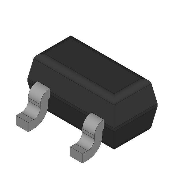
CASE 463
SOT−416/SC−75
STYLE 3
DEVICE MARKING
A4
1. FR−4 @ Minimum Pad
2. FR−4 @ 1.0 × 1.0 Inch Pad
ORDERING INFORMATION
Device
Package
Shipping†
BAV70TT1
SOT−416
3000 / Tape & Reel
BAV70TT1G
SOT−416
(Pb-Free)
3000 / Tape & Reel
†For information on tape and reel specifications,
including part orientation and tape sizes, please
refer to our Tape and Reel Packaging Specifications
Brochure, BRD8011/D.
*For additional information on our Pb−Free strategy
and soldering details, please download the
ON Semiconductor Soldering and Mounting
Techniques Reference Manual, SOLDERRM/D.
Preferred devices are recommended choices for future use
and best overall value.
Semiconductor Components Industries, LLC, 2003
December, 2003 − Rev. 2
242
Publication Order Number:
BAV70TT1/D
�BAV70TT1
ELECTRICAL CHARACTERISTICS (TA = 25°C unless otherwise noted)
Characteristic
Symbol
Min
Max
Unit
V(BR)
70
−
Vdc
IR
IR
−
−
5.0
100
�Adc
nAdc
Diode Capacitance
(VR = 0, f = 1.0 MHz)
CD
−
1.5
pF
Forward Voltage
(IF = 1.0 mAdc)
(IF = 10 mAdc)
(IF = 50 mAdc)
(IF = 150 mAdc)
VF
−
−
−
−
715
855
1000
1250
Reverse Recovery Time
(IF = IR = 10 mAdc, RL = 100 �, IR(REC) = 1.0 mAdc) (Figure 1)
trr
−
6.0
ns
VRF
−
1.75
V
OFF CHARACTERISTICS
Reverse Breakdown Voltage
(I(BR) = 100 �Adc)
Reverse Voltage Leakage Current (Note 3)
(VR = 70 Vdc)
(VR = 50 Vdc)
Forward Recovery Voltage
(IF = 10 mAdc, tr = 20 ns) (Figure 2)
3. For each individual diode while the second diode is unbiased.
http://onsemi.com
243
mVdc
�BAV70TT1
7�-)�
�� 5 !� �
���%6���
���66 �� %�
�6 5 !� �
��
?,
?;
�
��>
8��
?,,
��>G �G
3�>
-�
�%
� %
6��
��%
� %
6��
Figure 1. Recovery Time Equivalent Test Circuit
� C�
1!� �
�� 5 !� �
���%6���
���66 �� %�
�6 5 !� �
7�-)�
�
3�>
-��
��>
?
?,
?;
��%
� %
6��
Figure 2.
http://onsemi.com
244
�%
� %
6��
?
-�
���G�
�BAV70TT1
��
�� �$��-����$�
�����$�µ��
���$� �*���$�
�����$�&��
���
��
�� 5 2!°�
�� 5
!°�
�"�
�� 5 =�1�°�
�"�
�"
�"1
�"4
�"2
�"�
-�� � �*��� - 6���� �- 6���
�� 5 �
!°�
�"�
�� 5 2!°�
�"�
�� 5 !!°�
�"��
�"���
�"
�� 5 �!�°�
�� 5
!°�
�
��
Figure 3. Forward Voltage
�
��
1�
-�� ��-���� - 6���� �- 6���
!�
Figure 4. Leakage Current
���$�� ��$��%��������$�;��
�"�
�"3
�"2
�")
�"4
�
1
4
2
-�� ��-���� - 6���� �- 6���
,�?��$� ���6�E��$���������$������6$����������
Figure 5. Capacitance
�"�
�"�
� 5 �"!
�"
�"�
�"�!
�"�
�"��
�"��
����6� %
6��
�"���
�"�����
�"����
�"���
�"��
�"�
�"�
?� ���� ���
Figure 6. Normalized Thermal Response
http://onsemi.com
245
��
���
����
�
很抱歉,暂时无法提供与“BAV70TT1”相匹配的价格&库存,您可以联系我们找货
免费人工找货- 国内价格 香港价格
- 3040+1.051513040+0.13574
- 10000+0.9373210000+0.12100
- 100000+0.78480100000+0.10131