DATA SHEET
www.onsemi.com
Dual Series Switching
Diodes
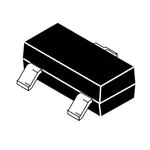
SC−70
CASE 419
BAV99W, BAV99RW
The BAV99WT1G is a smaller package, equivalent to the
BAV99LT1G.
ANODE
1
Features
3
CATHODE/ANODE
• S and NSV Prefix for Automotive and Other Applications Requiring
•
CATHODE
2
Unique Site and Control Change Requirements; AEC−Q101
Qualified and PPAP Capable
These Devices are Pb−Free, Halogen Free/BFR Free and are RoHS
Compliant*
BAV99WT1
SC−70, CASE 419, STYLE 9
CATHODE
1
Suggested Applications
•
•
•
•
•
3
CATHODE/ANODE
ESD Protection
Polarity Reversal Protection
Data Line Protection
Inductive Load Protection
Steering Logic
BAV99RWT1
SC−70, CASE 419, STYLE 10
MARKING DIAGRAM
X7 MG
G
MAXIMUM RATINGS (Each Diode)
Rating
Reverse Voltage
Forward Current
1
Symbol
Value
Unit
VR
100
Vdc
IF
215
mAdc
IFM(surge)
500
mAdc
Repetitive Peak Reverse Voltage
VRRM
100
V
Average Rectified Forward Current
(Note 1)
(averaged over any 20 ms period)
IF(AV)
715
mA
Repetitive Peak Forward Current
IFRM
450
mA
Non−Repetitive Peak Forward Current
t = 1.0 ms
t = 1.0 ms
t = 1.0 s
IFSM
Peak Forward Surge Current
A
2.0
1.0
0.5
Stresses exceeding those listed in the Maximum Ratings table may damage the
device. If any of these limits are exceeded, device functionality should not be
assumed, damage may occur and reliability may be affected.
1. FR−5 = 1.0 � 0.75 � 0.062 in.
© Semiconductor Components Industries, LLC, 2015
February, 2022 − Rev. 11
ANODE
2
1
A7
F7
M
G
= BAV99W
= BAV99RW
= Date Code
= Pb−Free Package
ORDERING INFORMATION
Package
Shipping†
BAV99WT1G
SC−70
(Pb−Free)
3,000 / Tape & Reel
SBAV99WT1G
SC−70
(Pb−Free)
3,000 / Tape & Reel
BAV99RWT1G
SC−70
(Pb−Free)
3,000 / Tape & Reel
SBAV99RWT1G
SC−70
(Pb−Free)
3,000 / Tape & Reel
BAV99WT3G
SC−70
10,000 / Tape & Reel
(Pb−Free)
NSVBAV99WT3G
SC−70
10,000 / Tape & Reel
(Pb−Free)
Device
†For information on tape and reel specifications,
including part orientation and tape sizes, please
refer to our Tape and Reel Packaging Specifications
Brochure, BRD8011/D.
Publication Order Number:
BAV99WT1/D
�BAV99W, BAV99RW
THERMAL CHARACTERISTICS
Characteristic
Symbol
Max
Unit
PD
200
1.6
mW
mW/°C
RqJA
625
°C/W
PD
300
2.4
mW
mW/°C
RqJA
417
°C/W
TJ, Tstg
−65 to +150
°C
Total Device Dissipation FR−5 Board, (Note 1) TA = 25°C
Derate above 25°C
Thermal Resistance Junction−to−Ambient
Total Device Dissipation Alumina Substrate, (Note 2) TA = 25°C
Derate above 25°C
Thermal Resistance Junction−to−Ambient
Junction and Storage Temperature
ELECTRICAL CHARACTERISTICS (TA = 25°C unless otherwise noted) (Each Diode)
Symbol
Characteristic
Min
Max
100
−
−
−
−
1.0
30
50
−
1.5
−
−
−
−
715
855
1000
1250
−
6.0
−
1.75
Unit
OFF CHARACTERISTICS
Reverse Breakdown Voltage
(I(BR) = 100 mA)
V(BR)
Reverse Voltage Leakage Current
(VR = 100 Vdc)
(VR = 25 Vdc, TJ = 150°C)
(VR = 70 Vdc, TJ = 150°C)
IR
Diode Capacitance
(VR = 0, f = 1.0 MHz)
CD
Forward Voltage
(IF = 1.0 mAdc)
(IF = 10 mAdc)
(IF = 50 mAdc)
(IF = 150 mAdc)
VF
Reverse Recovery Time
(IF = IR = 10 mAdc, iR(REC) = 1.0 mAdc) (Figure 1) RL = 100 W
trr
Forward Recovery Voltage
(IF = 10 mA, tr = 20 ns)
VFR
Vdc
mAdc
pF
mVdc
ns
V
Product parametric performance is indicated in the Electrical Characteristics for the listed test conditions, unless otherwise noted. Product
performance may not be indicated by the Electrical Characteristics if operated under different conditions.
1. FR−5 = 1.0 � 0.75 � 0.062 in.
2. Alumina = 0.4 � 0.3 � 0.024 in. 99.5% alumina.
820 W
+10 V
2k
100 mH
0.1 mF
IF
tr
tp
0.1 mF
t
IF
trr
10%
t
DUT
50 W OUTPUT
PULSE
GENERATOR
90%
50 W INPUT
SAMPLING
OSCILLOSCOPE
IR
VR
INPUT SIGNAL
Notes: (a) A 2.0 kW variable resistor adjusted for a Forward Current (IF) of 10 mA.
Notes: (b) Input pulse is adjusted so IR(peak) is equal to 10 mA.
Notes: (c) tp » trr
Figure 1. Recovery Time Equivalent Test Circuit
www.onsemi.com
2
iR(REC) = 1 mA
OUTPUT PULSE
(IF = IR = 10 mA; measured
at iR(REC) = 1 mA)
�BAV99W, BAV99RW
CURVES APPLICABLE TO EACH DIODE
1000
10
I R, REVERSE CURRENT (��A)
μ
100
10
TA = 150°C TA = 25°C
1.0
TA = -�55°C
TA = 125°C
1.0
TA = 85°C
0.1
TA = 55°C
0.01
TA = 25°C
0.1
0.0
0.2
0.4
0.6
0.8
VF, FORWARD VOLTAGE (VOLTS)
1.0
0.001
1.2
10
0
Figure 2. Forward Voltage
20
30
40
VR, REVERSE VOLTAGE (VOLTS)
Figure 3. Leakage Current
0.68
CD , DIODE CAPACITANCE (pF)
IF, FORWARD CURRENT (mA)
TA = 150°C
0.64
0.60
0.56
0.52
0
2
4
6
VR, REVERSE VOLTAGE (VOLTS)
Figure 4. Capacitance
www.onsemi.com
3
8
50
�MECHANICAL CASE OUTLINE
PACKAGE DIMENSIONS
SC−70 (SOT−323)
CASE 419
ISSUE R
DATE 11 OCT 2022
SCALE 4:1
GENERIC
MARKING DIAGRAM
XX MG
G
1
XX
M
G
= Specific Device Code
= Date Code
= Pb−Free Package
*This information is generic. Please refer to
device data sheet for actual part marking.
Pb−Free indicator, “G” or microdot “G”, may
or may not be present. Some products may
not follow the Generic Marking.
STYLE 1:
CANCELLED
STYLE 6:
PIN 1. EMITTER
2. BASE
3. COLLECTOR
DOCUMENT NUMBER:
DESCRIPTION:
STYLE 2:
PIN 1. ANODE
2. N.C.
3. CATHODE
STYLE 3:
PIN 1. BASE
2. EMITTER
3. COLLECTOR
STYLE 4:
PIN 1. CATHODE
2. CATHODE
3. ANODE
STYLE 5:
PIN 1. ANODE
2. ANODE
3. CATHODE
STYLE 7:
PIN 1. BASE
2. EMITTER
3. COLLECTOR
STYLE 8:
PIN 1. GATE
2. SOURCE
3. DRAIN
STYLE 9:
PIN 1. ANODE
2. CATHODE
3. CATHODE-ANODE
STYLE 10:
PIN 1. CATHODE
2. ANODE
3. ANODE-CATHODE
98ASB42819B
SC−70 (SOT−323)
STYLE 11:
PIN 1. CATHODE
2. CATHODE
3. CATHODE
Electronic versions are uncontrolled except when accessed directly from the Document Repository.
Printed versions are uncontrolled except when stamped “CONTROLLED COPY” in red.
PAGE 1 OF 1
onsemi and
are trademarks of Semiconductor Components Industries, LLC dba onsemi or its subsidiaries in the United States and/or other countries. onsemi reserves
the right to make changes without further notice to any products herein. onsemi makes no warranty, representation or guarantee regarding the suitability of its products for any particular
purpose, nor does onsemi assume any liability arising out of the application or use of any product or circuit, and specifically disclaims any and all liability, including without limitation
special, consequential or incidental damages. onsemi does not convey any license under its patent rights nor the rights of others.
© Semiconductor Components Industries, LLC, 2019
www.onsemi.com
�onsemi,
, and other names, marks, and brands are registered and/or common law trademarks of Semiconductor Components Industries, LLC dba “onsemi” or its affiliates
and/or subsidiaries in the United States and/or other countries. onsemi owns the rights to a number of patents, trademarks, copyrights, trade secrets, and other intellectual property.
A listing of onsemi’s product/patent coverage may be accessed at www.onsemi.com/site/pdf/Patent−Marking.pdf. onsemi reserves the right to make changes at any time to any
products or information herein, without notice. The information herein is provided “as−is” and onsemi makes no warranty, representation or guarantee regarding the accuracy of the
information, product features, availability, functionality, or suitability of its products for any particular purpose, nor does onsemi assume any liability arising out of the application or use
of any product or circuit, and specifically disclaims any and all liability, including without limitation special, consequential or incidental damages. Buyer is responsible for its products
and applications using onsemi products, including compliance with all laws, regulations and safety requirements or standards, regardless of any support or applications information
provided by onsemi. “Typical” parameters which may be provided in onsemi data sheets and/or specifications can and do vary in different applications and actual performance may
vary over time. All operating parameters, including “Typicals” must be validated for each customer application by customer’s technical experts. onsemi does not convey any license
under any of its intellectual property rights nor the rights of others. onsemi products are not designed, intended, or authorized for use as a critical component in life support systems
or any FDA Class 3 medical devices or medical devices with a same or similar classification in a foreign jurisdiction or any devices intended for implantation in the human body. Should
Buyer purchase or use onsemi products for any such unintended or unauthorized application, Buyer shall indemnify and hold onsemi and its officers, employees, subsidiaries, affiliates,
and distributors harmless against all claims, costs, damages, and expenses, and reasonable attorney fees arising out of, directly or indirectly, any claim of personal injury or death
associated with such unintended or unauthorized use, even if such claim alleges that onsemi was negligent regarding the design or manufacture of the part. onsemi is an Equal
Opportunity/Affirmative Action Employer. This literature is subject to all applicable copyright laws and is not for resale in any manner.
PUBLICATION ORDERING INFORMATION
LITERATURE FULFILLMENT:
Email Requests to: orderlit@onsemi.com
onsemi Website: www.onsemi.com
◊
TECHNICAL SUPPORT
North American Technical Support:
Voice Mail: 1 800−282−9855 Toll Free USA/Canada
Phone: 011 421 33 790 2910
Europe, Middle East and Africa Technical Support:
Phone: 00421 33 790 2910
For additional information, please contact your local Sales Representative
�