Ordering number : ENA1356A
BBL4001
N-Channel Power MOSFET
http://onsemi.com
60V, 74A, 6.1mΩ, TO-220F-3SG
Features
•
•
•
ON-resistance RDS(on)1=4.7mΩ(typ.)
Input capacitance Ciss=6,900pF(typ.)
4V drive
Specifications
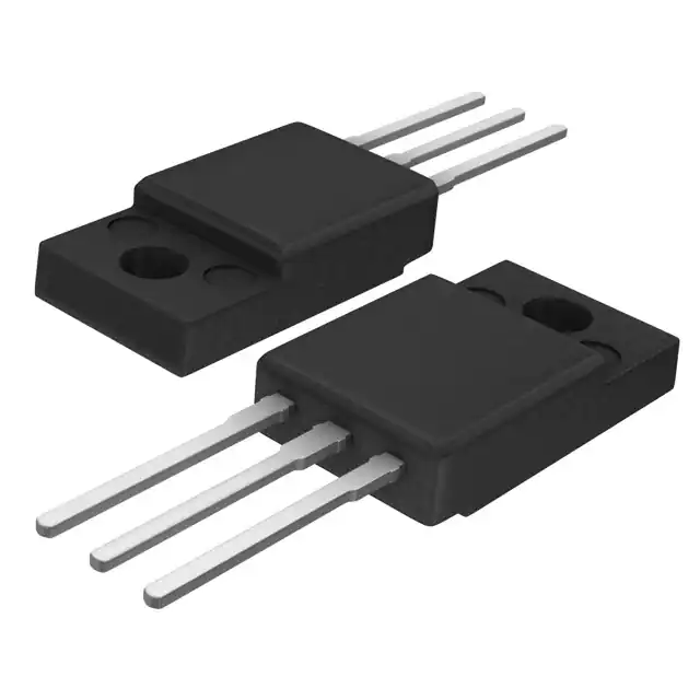
TO-220F-3SG
Absolute Maximum Ratings at Ta=25°C
Parameter
Drain to Source Voltage
Gate to Source Voltage
Drain Current (DC)
Drain Current (Pulse)
Symbol
Conditions
Ratings
VDSS
VGSS
ID
IDP
Unit
60
PW≤10μs, duty cycle≤1%
V
±20
V
74
A
296
A
2.0
W
Allowable Power Dissipation
PD
Junction Temperature
Tj
Storage Temperature
Tstg
--55 to +150
°C
Avalanche Energy (Single Pulse) *1
EAS
IAV
370
mJ
65
A
Avalanche Current *2
Tc=25°C
35
W
150
°C
Note : *1 VDD=30V, L=100μH, IAV=65A(Fig.1)
*2 L≤100μH, Single pulse
Stresses exceeding those listed in the Maximum Ratings table may damage the device. If any of these limits are exceeded, device functionality should not be assumed,
damage may occur and reliability may be affected.
Electrical Characteristics at Ta=25°C
Parameter
Symbol
Conditions
Ratings
min
typ
60
Drain to Source Breakdown Voltage
V(BR)DSS
Zero-Gate Voltage Drain Current
IDSS
ID=1mA, VGS=0V
VDS=60V, VGS=0V
Gate to Source Leakage Current
IGSS
VGS=±16V, VDS=0V
Gate Threshold Voltage
VGS(th)
VDS=10V, ID=1mA
1.2
Forward Transconductance
gFS
VDS=10V, ID=37A
32
Static Drain to Source On-State Resistance
RDS(on)1
RDS(on)2
ID=37A, VGS=10V
ID=37A, VGS=4V
Input Capacitance
Ciss
Output Capacitance
Coss
Reverse Transfer Capacitance
Turn-ON Delay Time
Rise Time
Turn-OFF Delay Time
Unit
max
V
1
μA
±10
μA
2.6
53
V
S
4.7
6.1
mΩ
7.0
9.8
mΩ
6900
pF
740
pF
Crss
540
pF
td(on)
tr
48
ns
300
ns
510
ns
Fall Time
td(off)
tf
Total Gate Charge
Qg
Gate to Source Charge
Qgs
Gate to Drain “Miller” Charge
Qgd
Diode Forward Voltage
VSD
VDS=20V, f=1MHz
See specified Test Circuit.
VDS=30V, VGS=10V, ID=74A
340
ns
135
nC
18
nC
32
IS=74A, VGS=0V
1.0
nC
1.2
V
Product parametric performance is indicated in the Electrical Characteristics for the listed test conditions, unless otherwise noted. Product performance may not be
indicated by the Electrical Characteristics if operated under different conditions.
ORDERING INFORMATION
See detailed ordering and shipping information on page 4 of this data sheet.
Semiconductor Components Industries, LLC, 2014
April, 2014
40214 TKIM TC-00003095 / N2608QA TI IM TC-00001754 No. A1356-1/5
�BBL4001
Tc= -25°C
75°C
VDS=10V
10
4V
120
30
25
°C
30
C
60
--25
°
60
90
5°C
90
Tc=
7
Drain Current, ID -- A
Drain Current, ID -- A
120
ID -- VGS(th)
150
6V
V 8
V
Tc=25°C
25°C
ID -- VDS
150
VGS=3V
0.6
0.8
1.0
1.2
Drain to Source Voltage, VDS -- V
Static Drain to Source
On-State Resistance, RDS(on) -- mΩ
12
10
8
Tc=75°C
6
25°C
4
--25°C
2
0
0
1
2
3
4
5
6
7
8
9
Gate to Source Voltage, VGS -- V
°C
C
5°
10
=
Tc
7
--2
°C
75
5
3
2
3
5 7 1.0
3
2
5 7 10
2
3
Drain Current, ID -- A
5 7 100
8
6
VDD=30V
VGS=10V
4.5
IT14162
4
2
--25
0
25
50
75
100
125
150
IT14164
IS -- VSD
VGS=0V
Single pulse
10
7
5
3
2
1.0
7
5
3
2
0.1
7
5
3
2
0
0.2
0.4
0.6
0.8
1.0
1.2
1.4
IT14166
Ciss, Coss, Crss -- VDS
5
td(off)
4.0
Diode Forward Voltage, VSD -- V
f=1MHz
3
2
5
3
10000
7
5
Ciss, Coss, Crss -- pF
Switching Time, SW Time -- ns
7
3.5
37A
I D=
,
V
=4
V GS
A
=37
V, I D
0
1
=
VGS
IT14165
SW Time -- ID
1000
10
0.01
7
5
3
2
0.001
2
1.0
0.1
3.0
12
100
7
5
3
2
25
2.5
Single pulse
3
2
5
2
2.0
Case Temperature, Tc -- °C
VDS=10V
3
1.5
RDS(on) -- Tc
0
--50
10
Source Current, IS -- A
Forward Transconductance, gFS -- S
7
1.0
Gate to Source Voltage, VGS -- V
IT14163
gFS -- ID
100
0.5
14
ID=37A
Single pulse
14
0
IT14161
RDS(on) -- VGS
16
0
1.4
--25°
C
0.4
5°C
25°C
0.2
Tc=
7
0
Static Drain to Source
On-State Resistance, RDS(on) -- mΩ
0
tf
2
100
tr
7
3
0.1
3
2
1000
Coss
7
5
Crss
3
td(on)
5
Ciss
2
2
3
5 7 1.0
2
3
5 7 10
Drain Current, ID -- A
2
3
5 7 100
IT14167
100
0
5
10
15
20
25
Drain to Source Voltage, VDS -- V
30
IT14168
No. A1356-2/5
�BBL4001
VGS -- Qg
10
8
Drain Current, ID -- A
Gate to Source Voltage, VGS -- V
9
7
6
5
4
3
2
1
0
0
50
100
PD -- Ta
Allowable Power Dissipation, PD -- W
Allowable Power Dissipation, PD -- W
0.5
40
60
80
100
120
140
Ambient Temperature, Ta -- °C
Avalanche Energy derating factor -- %
1.0
7
5
3
2
s
ms
Tc=25°C
Single pulse
2
3
5 7 1.0
2
3
5 7 10
2
3
PD -- Tc
30
25
20
15
10
5
0
160
5 7 100
IT14170
35
0
20
40
60
80
100
120
140
Case Temperature, Tc -- °C
IT14158
EAS -- Ta
120
10
Operation in
DC
0m
op
s
this area is
era
tio
limited by RDS(on).
n
40
1.0
20
1m
10
10
7
5
3
2
μs
0μ
s
Drain to Source Voltage, VDS -- V
1.5
0
10
10
ID=74A
100
7
5
3
2
IT14169
2.0
0
IDP=296A (PW≤10μs)
0.1
0.1
150
Total Gate Charge, Qg -- nC
2.5
SOA
7
5
3
2
VDS=30V
ID=74A
160
IT14159
100
80
60
40
20
0
0
25
50
75
100
125
150
Ambient Temperature, Ta -- °C
RθJC -- Pulse Time
10
Thermal Resistance, RθJC -- ºC/W
175
IT14160
Duty Cycle=0.5
0.2
0.1
0.05
1.0
0.02
0.01
0.1
lse
le Pu
0.01
Sing
0.001
0.000001 2
3
5 70.00001 2
3
5 70.0001
2
3
5 7 0.001
2
3
5 7 0.01
Pulse Time, PT -- s
2
3
5
7 0.1
2
3
5
7 1
2
3
5
7 10
IT17539
No. A1356-3/5
�BBL4001
Package Dimensions
BBL4001-1E
TO-220 Fullpack, 3-Lead / TO-220F-3SG
CASE 221AT
ISSUE A
unit : mm
1: Gate
2: Drain
3: Source
Marking
Ordering & Package Information
Device
Package
Shipping
memo
BBL4001-1E
TO-220F-3SG
SC-67
50
pcs. / tube
Pb-Free
Electrical Connection
2
BL4001
LOT No.
1
3
No. A1356-4/5
�BBL4001
Fig.1 Unclamped Inductive Switching Test Circuit
L
Fig.2 Switching Time Test Circuit
10V
0V
≥50Ω
50Ω
ID=37A
RL=0.81Ω
VIN
BBL4001
10V
0V
VDD=30V
VIN
VDD
D
PW=10μs
D.C.≤1%
VOUT
G
BBL4001
P.G
50Ω
S
Note on usage : Since the BBL4001 is a MOSFET product, please avoid using this device in the vicinity of
highly charged objects.
ON Semiconductor and the ON logo are registered trademarks of Semiconductor Components Industries, LLC (SCILLC). SCILLC owns the rights to a number
of patents, trademarks, copyrights, trade secrets, and other intellectual property. A listing of SCILLC’s product/patent coverage may be accessed at
www.onsemi.com/site/pdf/Patent-Marking.pdf. SCILLC reserves the right to make changes without further notice to any products herein. SCILLC makes no
warranty, representation or guarantee regarding the suitability of its products for any particular purpose, nor does SCILLC assume any liability arising out of the
application or use of any product or circuit, and specifically disclaims any and all liability, including without limitation special, consequential or incidental
damages. “Typical” parameters which may be provided in SCILLC data sheets and/or specifications can and do vary in different applications and actual
performance may vary over time. All operating parameters, including “Typicals” must be validated for each customer application by customer’s technical
experts. SCILLC does not convey any license under its patent rights nor the rights of others. SCILLC products are not designed, intended, or authorized for use
as components in systems intended for surgical implant into the body, or other applications intended to support or sustain life, or for any other application in
which the failure of the SCILLC product could create a situation where personal injury or death may occur. Should Buyer purchase or use SCILLC products for
any such unintended or unauthorized application, Buyer shall indemnify and hold SCILLC and its officers, employees, subsidiaries, affiliates, and distributors
harmless against all claims, costs, damages, and expenses, and reasonable attorney fees arising out of, directly or indirectly, any claim of personal injury or
death associated with such unintended or unauthorized use, even if such claim alleges that SCILLC was negligent regarding the design or manufacture of the
part. SCILLC is an Equal Opportunity/Affirmative Action Employer. This literature is subject to all applicable copyright laws and is not for resale in any manner.
PS No. A1356-5/5
�