Features
•
•
•
•
3
Switching and Amplifier Applications
Suitable for Automatic Insertion in Thick and Thin-film Circuits
Low Noise: BC850
Complement to BC856, BC857, BC858, BC859, and BC860
2
1
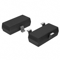
SOT-23
1. Base 2. Emitter 3. Collector
Ordering Information(1)
Part Number
Marking
Package
Packing Method
BC846AMTF
8AA
SOT-23 3L
Tape and Reel
BC846BMTF
8AB
SOT-23 3L
Tape and Reel
BC846CMTF
8AC
SOT-23 3L
Tape and Reel
BC847AMTF
8BA
SOT-23 3L
Tape and Reel
BC847BMTF
8BB
SOT-23 3L
Tape and Reel
BC847CMTF
8BC
SOT-23 3L
Tape and Reel
BC848BMTF
8CB
SOT-23 3L
Tape and Reel
BC848CMTF
8CC
SOT-23 3L
Tape and Reel
BC850AMTF
8EA
SOT-23 3L
Tape and Reel
BC850CMTF
8EC
SOT-23 3L
Tape and Reel
Note:
1. Affix “-A,-B,-C” means hFE classification. Affix “-M” means SOT-23 package. Affix “-TF” means the tape and reel type
packing.
© 2002 Semiconductor Components Industries, LLC.
September-2017, Rev. 2
1
Publication Order Number:
BC846/D
BC846 / BC847 / BC848 / BC850 — NPN Epitaxial Silicon Transistor
BC846 / BC847 / BC848 / BC850
NPN Epitaxial Silicon Transistor
�Stresses exceeding the absolute maximum ratings may damage the device. The device may not function or be operable above the recommended operating conditions and stressing the parts to these levels is not recommended. In addition, extended exposure to stresses above the recommended operating conditions may affect device reliability. The
absolute maximum ratings are stress ratings only. Values are at TA = 25°C unless otherwise noted.
Symbol
VCBO
VCEO
Parameter
Collector-Base Voltage
Collector-Emitter Voltage
VEBO
Emitter-Base Voltage
IC
Collector Current (DC)
TJ
Junction Temperature
TSTG
Value
BC846
80
BC847 / BC850
50
BC848
30
BC846
65
BC847 / BC850
45
BC848
30
BC846 / BC847
6
BC848 / BC850
5
Unit
V
V
V
100
mA
150
°C
-65 to +150
°C
Value
Unit
Power Dissipation
310
mW
Derate Above 25°C
2.48
mW/°C
Thermal Resistance, Junction-to-Ambient
403
°C/W
Storage Temperature Range
Thermal Characteristics(2)
Values are at TA = 25°C unless otherwise noted.
Symbol
PD
RθJA
Parameter
Note:
2. PCB size: FR-4, 76 mm x 114 mm x 1.57 mm (3.0 inch x 4.5 inch x 0.062 inch) with minimum land pattern size.
www.onsemi.com
2
BC846 / BC847 / BC848 / BC850 — NPN Epitaxial Silicon Transistor
Absolute Maximum Ratings
�Values are at TA = 25°C unless otherwise noted.
Symbol
Parameter
Conditions
Min.
Typ.
Max.
Unit
15
nA
ICBO
Collector Cut-Off Current
VCB = 30 V, IE = 0
hFE
DC Current Gain
VCE = 5 V, IC = 2 mA
VCE(sat)
Collector-Emitter Saturation
Voltage
IC = 10 mA, IB = 0.5 mA
90
250
IC = 100 mA, IB = 5 mA
200
600
VBE(sat)
Collector-Base Saturation Voltage
VBE(on)
Base-Emitter On Voltage
110
800
IC = 10 mA, IB = 0.5 mA
700
IC = 100 mA, IB = 5 mA
900
VCE = 5 V, IC = 2 mA
580
660
VCE = 5 V, IC = 10 mA
VCE = 5 V, IC = 10 mA,
f = 100 MHz
300
Cob
Output Capacitance
VCB = 10 V, IE = 0, f = 1 MHz
3.5
Cib
Input Capacitance
VEB = 0.5 V, IC = 0, f = 1 MHz
NF
Noise
Figure
BC846 / BC847 / BC848 VCE = 5 V, IC = 200 μA,
RG = 2 kΩ, f = 1 kHz
BC850
VCE = 5 V, IC = 200 μA,
RG = 2 kΩ, f = 30 to 15000 Hz
BC850
mV
700
720
Current Gain Bandwidth Product
fT
mV
MHz
6.0
9
pF
pF
2.0
10.0
1.2
4.0
1.4
3.0
Note:
3. Pulse test: pulse width ≤ 300 μs, duty cycle ≤ 2%
hFE Classification
Classification
A
B
C
hFE
110 ~ 220
200 ~ 450
420 ~ 800
www.onsemi.com
3
mV
dB
BC846 / BC847 / BC848 / BC850 — NPN Epitaxial Silicon Transistor
Electrical Characteristics(3)
�1000
IB = 400μA
IB = 350μA
80
IB = 300μA
IB = 250μA
60
VCE = 5V
o
TA = 150 C
hFE, DC CURRENT GAIN
IC[mA], COLLECTOR CURRENT
100
IB = 200μA
IB = 150μA
40
IB = 100μA
o
TA = 25 C
100
o
TA = -55 C
20
IB = 50μA
10
0.1
0
0
4
8
12
16
20
VCE[V], COLLECTOR-EMITTER VOLTAGE
Figure 1. Static Characteristic
1000
0.1
o
TA = 150 C
o
TA = 25 C
o
TA = -55 C
0.01
0.1
1
10
100
IC = 20IB
SATURATION VOLTAGE
VCE(SAT) [V], COLLECTOR-EMITTER
SATURATION VOLTAGE
VCE(SAT) [V], COLLECTOR-EMITTER
100
10
IC = 10IB
1
0.1
0.01
0.1
1.0
o
TA = -55 C
o
TA = 25 C
o
TA = 150 C
1
10
100
10
100
1000
1000
Figure 4. Collector-Emitter Saturation Voltage
VBE(SAT) [V], BASE-EMITTER SATURATION VOLTAGE
IC = 10IB
0.4
1
IC [mA], COLLECTOR CURRENT
1.2
0.6
TA = 25 C
o
TA = -55 C
1000
Figure 3. Collector-Emitter Saturation Voltage
0.8
o
TA = 150 C
o
IC [mA], COLLECTOR CURRENT
VBE(SAT) [V], BASE-EMITTER SATURATION VOLTAGE
10
Figure 2. DC Current Gain
1
0.2
0.1
1
IC [mA], COLLECTOR CURRENT
IC [mA], COLLECTOR CURRENT
1.2
IC = 20IB
1.0
0.8
o
TA = -55 C
o
TA = 25 C
0.6
0.4
0.2
0.1
o
TA = 150 C
1
10
100
1000
IC [mA], COLLECTOR CURRENT
Figure 5. Base-Emitter Saturation Voltage
www.onsemi.com
4
Figure 6. Base-Emitter Saturation Voltage
BC846 / BC847 / BC848 / BC850 — NPN Epitaxial Silicon Transistor
Typical Performance Characteristics
�100
VCE = 5V
f=1MHz
Cob[pF], CAPACITANCE
IC [mA], COLLECTOR CURRENT
100
10
o
o
TA = 150 C
1
0.1
0.0
o
TA = 25 C
TA = -55 C
0.4
0.6
0.8
1.0
1.2
1
VCE=5V
100
10
10
100
Figure 8. Collector Output Capacitance
1000
1
10
VCB[V], COLLECTOR-BASE VOLTAGE
Figure 7. Base-Emitter On Voltage
fT[MHz], CURRENT GAIN-BANDWIDTH PRODUCT
1
0.1
0.2
VBE(ON) [V], BASE-EMITTER ON VOLTAGE
1
0.1
10
100
IC[mA], COLLECTOR CURRENT
Figure 9. Current Gain Bandwidth Product
www.onsemi.com
5
1000
BC846 / BC847 / BC848 / BC850 — NPN Epitaxial Silicon Transistor
Typical Performance Characteristics (Continued)
�ON Semiconductor and
are trademarks of Semiconductor Components Industries, LLC dba ON Semiconductor or its subsidiaries in the United States and/or other countries.
ON Semiconductor owns the rights to a number of patents, trademarks, copyrights, trade secrets, and other intellectual property. A listing of ON Semiconductor’s product/patent
coverage may be accessed at www.onsemi.com/site/pdf/Patent−Marking.pdf. ON Semiconductor reserves the right to make changes without further notice to any products herein.
ON Semiconductor makes no warranty, representation or guarantee regarding the suitability of its products for any particular purpose, nor does ON Semiconductor assume any liability
arising out of the application or use of any product or circuit, and specifically disclaims any and all liability, including without limitation special, consequential or incidental damages.
Buyer is responsible for its products and applications using ON Semiconductor products, including compliance with all laws, regulations and safety requirements or standards,
regardless of any support or applications information provided by ON Semiconductor. “Typical” parameters which may be provided in ON Semiconductor data sheets and/or
specifications can and do vary in different applications and actual performance may vary over time. All operating parameters, including “Typicals” must be validated for each customer
application by customer’s technical experts. ON Semiconductor does not convey any license under its patent rights nor the rights of others. ON Semiconductor products are not
designed, intended, or authorized for use as a critical component in life support systems or any FDA Class 3 medical devices or medical devices with a same or similar classification
in a foreign jurisdiction or any devices intended for implantation in the human body. Should Buyer purchase or use ON Semiconductor products for any such unintended or unauthorized
application, Buyer shall indemnify and hold ON Semiconductor and its officers, employees, subsidiaries, affiliates, and distributors harmless against all claims, costs, damages, and
expenses, and reasonable attorney fees arising out of, directly or indirectly, any claim of personal injury or death associated with such unintended or unauthorized use, even if such
claim alleges that ON Semiconductor was negligent regarding the design or manufacture of the part. ON Semiconductor is an Equal Opportunity/Affirmative Action Employer. This
literature is subject to all applicable copyright laws and is not for resale in any manner.
PUBLICATION ORDERING INFORMATION
LITERATURE FULFILLMENT:
Literature Distribution Center for ON Semiconductor
19521 E. 32nd Pkwy, Aurora, Colorado 80011 USA
Phone: 303−675−2175 or 800−344−3860 Toll Free USA/Canada
Fax: 303−675−2176 or 800−344−3867 Toll Free USA/Canada
Email: orderlit@onsemi.com
❖
© Semiconductor Components Industries, LLC
N. American Technical Support: 800−282−9855 Toll Free
USA/Canada
Europe, Middle East and Africa Technical Support:
Phone: 421 33 790 2910
Japan Customer Focus Center
Phone: 81−3−5817−1050
ON Semiconductor Website: www.onsemi.com
Order Literature: http://www.onsemi.com/orderlit
For additional information, please contact your local
Sales Representative
www.onsemi.com
�