ON Semiconductor
Is Now
To learn more about onsemi™, please visit our website at
www.onsemi.com
onsemi and and other names, marks, and brands are registered and/or common law trademarks of Semiconductor Components Industries, LLC dba “onsemi” or its affiliates and/or
subsidiaries in the United States and/or other countries. onsemi owns the rights to a number of patents, trademarks, copyrights, trade secrets, and other intellectual property. A listing of onsemi
product/patent coverage may be accessed at www.onsemi.com/site/pdf/Patent-Marking.pdf. onsemi reserves the right to make changes at any time to any products or information herein, without
notice. The information herein is provided “as-is” and onsemi makes no warranty, representation or guarantee regarding the accuracy of the information, product features, availability, functionality,
or suitability of its products for any particular purpose, nor does onsemi assume any liability arising out of the application or use of any product or circuit, and specifically disclaims any and all
liability, including without limitation special, consequential or incidental damages. Buyer is responsible for its products and applications using onsemi products, including compliance with all laws,
regulations and safety requirements or standards, regardless of any support or applications information provided by onsemi. “Typical” parameters which may be provided in onsemi data sheets and/
or specifications can and do vary in different applications and actual performance may vary over time. All operating parameters, including “Typicals” must be validated for each customer application
by customer’s technical experts. onsemi does not convey any license under any of its intellectual property rights nor the rights of others. onsemi products are not designed, intended, or authorized
for use as a critical component in life support systems or any FDA Class 3 medical devices or medical devices with a same or similar classification in a foreign jurisdiction or any devices intended for
implantation in the human body. Should Buyer purchase or use onsemi products for any such unintended or unauthorized application, Buyer shall indemnify and hold onsemi and its officers, employees,
subsidiaries, affiliates, and distributors harmless against all claims, costs, damages, and expenses, and reasonable attorney fees arising out of, directly or indirectly, any claim of personal injury or death
associated with such unintended or unauthorized use, even if such claim alleges that onsemi was negligent regarding the design or manufacture of the part. onsemi is an Equal Opportunity/Affirmative
Action Employer. This literature is subject to all applicable copyright laws and is not for resale in any manner. Other names and brands may be claimed as the property of others.
�Features
• Complement to BD136, BD138 and BD140 respectively
Applications
• Medium Power Linear and Switching
1
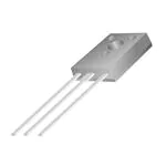
1. Emitter
TO-126
2.Collector
3.Base
Ordering Information
Part Number
Marking
BD13516S
BD1356STU
BD13510STU
BD13516STU
BD13716STU
BD13710STU
BD13716S
BD13916STU
BD13910S
BD13916S
BD1396STU
BD13910STU
BD135-16
BD135-6
BD135-10
BD135-16
BD137-16
BD137-10
BD137-16
BD139-16
BD139-10
BD139-16
BD139-6
BD139-10
© 2007 Semiconductor Components Industries, LLC.
November-2017, Rev. 2
Package
Packing Method
Bulk
Rail
TO-126 3L
Bulk
Rail
Bulk
Rail
Publication Order Number:
BD139/D
BD135 / 137 / 139 — NPN Epitaxial Silicon Transistor
BD135 / 137 / 139
NPN Epitaxial Silicon Transistor
�Stresses exceeding the absolute maximum ratings may damage the device. The device may not function or be operable above the recommended operating conditions and stressing the parts to these levels is not recommended. In addition, extended exposure to stresses above the recommended operating conditions may affect device reliability. The
absolute maximum ratings are stress ratings only. Values are at TC = 25°C unless otherwise noted.
Symbol
Parameter
VCBO
Collector-Base Voltage
VCEO
Collector-Emitter Voltage
VEBO
IC
ICP
IB
Emitter-Base Voltage
Collector Current (DC)
Collector Current (Pulse)
Base Current
PC
Device Dissipation
TJ
Junction Temperature
Storage Temperature
TSTG
Value
BD135
BD137
BD139
BD135
BD137
BD139
Units
45
60
80
45
60
80
5
1.5
3.0
0.5
12.5
1.25
150
- 55 to +150
TC = 25°C
TA = 25°C
V
V
V
A
A
A
W
W
°C
°C
Electrical Characteristics
Values are at TC = 25°C unless otherwise noted.
Symbol
VCEO(sus)
ICBO
IEBO
hFE1
hFE2
hFE3
VCE(sat)
VBE(on)
Parameter
Test Condition
BD135
BD137
BD139
Collector-Emitter Sustaining
Voltage
Collector Cut-off Current
Emitter Cut-off Current
DC Current Gain
Collector-Emitter Saturation Voltage
Base-Emitter On Voltage
IC = 30 mA, IB = 0
VCB = 30 V, IE = 0
VEB = 5 V, IC = 0
VCE = 2 V, IC = 5 mA
VCE = 2 V, IC = 0.5 A
VCE = 2 V, IC = 150 mA
IC = 500 mA, IB = 50 mA
VCE = 2 V, IC = 0.5 A
Min.
Typ.
Max.
45
60
80
25
25
40
V
0.1
10
μA
μA
250
0.5
1
V
V
hFE Classification
Classification
6
10
16
hFE3
40 ~ 100
63 ~ 160
100 ~ 250
www.onsemi.com
2
Units
BD135 / 137 / 139 — Features
Absolute Maximum Ratings
�BD135 / 137 / 139 — Features
Typical Performance Characteristics
100
60
50
40
30
20
10
100
400
IB
350
300
250
200
150
100
50
0
1E-3
0
10
IC = 20 IB
70
450
IC = 10
hFE, DC CURRENT GAIN
80
500
VCE(sat)[mV], SATURATION VOLTAGE
V CE = 2V
90
1000
Figure 1. DC current Gain
0.1
10
10
1.0
IC MAX. (Pulsed)
)
(on
V
V BE
=5
V CE
0.7
0.6
0.5
0.4
0.1
0.01
0.1
1E-3
0.01
0.1
1
1
10
Figure 3. Base-Emitter Voltage
17.5
15.0
12.5
10.0
7.5
5.0
2.5
0.0
50
75
100
125
100
Figure 4. Safe Operating Area
20.0
25
10
VCE[V], COLLECTOR-EMITTER VOLTAGE
IC[A], COLLECTOR CURRENT
0
100us
BD139
BD137
BD135
0.3
1
DC
IC[A], COLLECTOR CURRENT
0.8
10us
IC MAX. (Continuous)
s
1m
t)
(sa
V BE 0 I B
1
IC =
0.9
0.2
PC[W], POWER DISSIPATION
1
Figure 2. Collector-Emitter Saturation Voltage
1.1
VBE[V], BASE-EMITTER VOLTAGE
0.01
IC[A], COLLECTOR CURRENT
IC [mA], COLLECTOR CURRENT
150
175
o
TC[ C], CASE TEMPERATURE
Figure 5. Power Derating
www.onsemi.com
3
�BD135 / 137 / 139 — Features
Physical Dimensions
TO-126 3L
����
����
�����������
������0$;
�������������
�����������
������
�����������
�����������
'
������������
������
�����������
�;
����
�����������
�;
����
�
352'8&7,21 7(50,1$/
/(1*7+��'�
&2'(
76678
���������
7678
���������
127(6��
121(
���$��7+,6�3$&.$*(�'2(6�127�&203/