ON Semiconductor
Is Now
To learn more about onsemi™, please visit our website at
www.onsemi.com
onsemi and and other names, marks, and brands are registered and/or common law trademarks of Semiconductor Components Industries, LLC dba “onsemi” or its affiliates and/or
subsidiaries in the United States and/or other countries. onsemi owns the rights to a number of patents, trademarks, copyrights, trade secrets, and other intellectual property. A listing of onsemi
product/patent coverage may be accessed at www.onsemi.com/site/pdf/Patent-Marking.pdf. onsemi reserves the right to make changes at any time to any products or information herein, without
notice. The information herein is provided “as-is” and onsemi makes no warranty, representation or guarantee regarding the accuracy of the information, product features, availability, functionality,
or suitability of its products for any particular purpose, nor does onsemi assume any liability arising out of the application or use of any product or circuit, and specifically disclaims any and all
liability, including without limitation special, consequential or incidental damages. Buyer is responsible for its products and applications using onsemi products, including compliance with all laws,
regulations and safety requirements or standards, regardless of any support or applications information provided by onsemi. “Typical” parameters which may be provided in onsemi data sheets and/
or specifications can and do vary in different applications and actual performance may vary over time. All operating parameters, including “Typicals” must be validated for each customer application
by customer’s technical experts. onsemi does not convey any license under any of its intellectual property rights nor the rights of others. onsemi products are not designed, intended, or authorized
for use as a critical component in life support systems or any FDA Class 3 medical devices or medical devices with a same or similar classification in a foreign jurisdiction or any devices intended for
implantation in the human body. Should Buyer purchase or use onsemi products for any such unintended or unauthorized application, Buyer shall indemnify and hold onsemi and its officers, employees,
subsidiaries, affiliates, and distributors harmless against all claims, costs, damages, and expenses, and reasonable attorney fees arising out of, directly or indirectly, any claim of personal injury or death
associated with such unintended or unauthorized use, even if such claim alleges that onsemi was negligent regarding the design or manufacture of the part. onsemi is an Equal Opportunity/Affirmative
Action Employer. This literature is subject to all applicable copyright laws and is not for resale in any manner. Other names and brands may be claimed as the property of others.
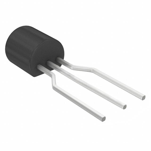
�BS270
N-Channel Enhancement Mode Field Effect Transistor
General Description
These N-Channel enhancement mode field effect transistors
are produced using ON Semiconductor's proprietary, high
cell density, DMOS technology. These products have been
designed to minimize on-state resistance while provide
rugged, reliable, and fast switching performance. They can
be used in most applications requiring up to 500mA DC.
These products are particularly suited for low voltage, low
current applications such as small servo motor control,
power MOSFET gate drivers, and other switching
applications.
Features
400mA, 60V. RDS(ON) = 2Ω @ VGS = 10V.
High density cell design for low RDS(ON).
Voltage controlled small signal switch.
Rugged and reliable.
High saturation current capability.
________________________________________________________________________________
D
G
S
Absolute Maximum Ratings
Symbol
Parameter
VDSS
T A = 25°C unless otherwise noted
BS270
Units
Drain-Source Voltage
60
V
VDGR
Drain-Gate Voltage (RGS < 1MΩ)
60
V
VGSS
Gate-Source Voltage - Continuous
±20
V
- Non Repetitive (tp < 50µs)
ID
Drain Current - Continuous
PD
Maximum Power Dissipation
- Pulsed
Derate Above 25°C
±40
400
mA
2000
625
mW
5
mW/°C
TJ,TSTG
Operating and Storage Temperature Range
-55 to 150
°C
TL
Maximum Lead Temperature for Soldering
Purposes, 1/16" from Case for 10 Seconds
300
°C
200
°C/W
THERMAL CHARACTERISTICS
RθJA
Thermal Resistacne, Junction-to-Ambient
© 1997 Semiconductor Components Industries, LLC.
September-2017, Rev. 2
Publication Order Number:
BS270/D
�Electrical Characteristics (TA = 25°C unless otherwise noted)
Symbol
Parameter
Conditions
Min
Typ
Max
Units
OFF CHARACTERISTICS
BVDSS
Drain-Source Breakdown Voltage
VGS = 0 V, ID = 10 µA
IDSS
Zero Gate Voltage Drain Current
VDS = 60 V, VGS = 0 V
60
V
TJ = 125oC
1
µA
500
µA
IGSSF
Gate - Body Leakage, Forward
VGS = 20 V, VDS = 0 V
10
nA
IGSSF
Gate - Body Leakage, Reverse
VGS = -20 V, VDS = 0 V
-10
nA
2.5
V
1.2
2
Ω
2
3.5
VGS = 4.5 V, ID = 75 mA
1.8
3
VGS = 10 V, ID = 500 mA
0.6
1
0.14
0.225
ON CHARACTERISTICS (Note 1)
VGS(th)
Gate Threshold Voltage
VDS = VGS, ID = 250 µA
RDS(ON)
Static Drain-Source On-Resistance
VGS = 10 V, ID = 500 mA
1
TJ = 125oC
VDS(ON)
Drain-Source On-Voltage
ID(ON)
On-State Drain Current
gFS
Forward Transconductance
VGS = 4.5 V, ID = 75 mA
VGS = 10 V, VDS > 2 VDS(on)
2000
2.1
2700
VGS = 4.5 V, VDS > 2 VDS(on)
400
600
VDS > 2 VDS(on), ID = 200 mA
100
320
V
mA
mS
DYNAMIC CHARACTERISTICS
Ciss
Input Capacitance
Coss
Output Capacitance
Crss
Reverse Transfer Capacitance
VDS = 25 V, VGS = 0 V,
f = 1.0 MHz
20
50
pF
11
25
pF
4
5
pF
10
ns
10
ns
400
mA
2000
mA
1.2
V
SWITCHING CHARACTERISTICS (Note 1)
ton
Turn-On Time
toff
Turn-Off Time
VDD = 30 V, ID = 500 m A,
VGS = 10 V, RGEN = 25 Ω
DRAIN-SOURCE DIODE CHARACTERISTICS AND MAXIMUM RATINGS
IS
Maximum Continuous Drain-Source Diode Forward Current
ISM
Maximum Pulsed Drain-Source Diode Forward Current
VSD
Drain-Source Diode Forward Voltage
VGS = 0 V, IS = 400 mA (Note 1)
Note:
1. Pulse Test: Pulse Width < 300µs, Duty Cycle < 2.0%.
www.onsemi.com
2
0.88
�Typical Electrical Characteristics
2
3
9.0
V GS =4.0V
8.0
, DRAIN-SOURCE CURRENT (A)
7.0
RDS(on) , NORMALIZED
1.5
6.0
1
5.0
0.5
I
D
4.0
DRAIN-SOURCE ON-RESISTANCE
VGS = 10V
3.0
0
0
1
2
3
V DS , DRAIN-SOURCE VOLTAGE (V)
4
5.0
6 .0
2
7.0
8.0
1.5
9.0
10
1
0.5
5
0
0.8
1.2
I D , DRAIN CURRENT (A)
1.6
2
Figure 2. On-Resistance Variation with Gate Voltage
and Drain Current.
2
3
1.75
V GS = 10V
R DS(on) , NORMALIZED
ID = 500mA
1.5
1.25
1
0.75
0.5
-50
-25
0
25
50
75
100
TJ , JUNCTION TEMPERATURE (°C)
125
DRAIN-SOURCE ON-RESISTANCE
R DS(ON) , NORMALIZED
DRAIN-SOURCE ON-RESISTANCE
0.4
Figure 1. On-Region Characteristics.
V G S = 10V
2.5
TJ = 125°C
2
1.5
25°C
1
-55°C
0.5
0
150
0
Figure 3. On-Resistance Variation
with Temperature.
0.4
0.8
1.2
I D , DRAIN CURRENT (A)
1.6
2
Figure 4. On-Resistance Variation with Drain
Current and Temperature.
1.1
VDS = 10V
T J = -55°C
25°C
125°C
Vth , NORMALIZED
1.6
1.2
0.8
0.4
0
0
2
V
GS
4
6
8
, GATE TO SOURCE VOLTAGE (V)
Figure 5. Transfer Characteristics.
10
GATE-SOURCE THRESHOLD VOLTAGE
2
ID , DRAIN CURRENT (A)
4.5
2.5
V DS = VGS
I D = 1 mA
1.05
1
0.95
0.9
0.85
0.8
-50
-25
0
25
50
75
100
TJ , JUNCTION TEMPERATURE (°C)
Figure 6. Gate Threshold Variation with
Temperature.
www.onsemi.com
3
125
150
�Typical Electrical Characteristics (continued)
2
ID = 10µA
1.05
1.025
1
0.975
0.95
0.925
-50
-25
0
25
50
75
100
TJ , JUNCTION TEMPERATURE (°C)
125
0.5
TJ = 125°C
0.1
25°C
0.05
-55°C
0.01
0.005
0.001
0.2
150
0.4
0.6
V SD
0.8
1
1.2
1.4
, BODY DIODE FORWARD VOLTAGE (V)
Figure 8. Body Diode Forward Voltage Variation with
Current and Temperature.
Figure 7. Breakdown Voltage Variation
with Temperature.
10
60
40
V GS , GATE-SOURCE VOLTAGE (V)
20
C oss
10
5
C rss
f = 1 MHz
V GS = 0V
2
V DS = 25V
ID = 5 0 0 m A
C iss
CAPACITANCE (pF)
V GS = 0V
1
1.075
IS , REVERSE DRAIN CURRENT (A)
, NORMALIZED
DSS
BV
DRAIN-SOURCE BREAKDOWN VOLTAGE
1.1
1
8
6
4
2
0
1
2
3
V DS
5
10
20
30
50
0
0.4
0.8
, DRAIN TO SOURCE VOLTAGE (V)
Figure 9. Capacitance Characteristics.
t on
t d(on)
R GEN
t d(off)
tf
90%
90%
V OUT
Output, Vout
10%
10%
90%
DUT
G
Input, Vin
50%
50%
10%
S
Figure 11. Switching Test Circuit.
2
t off
tr
RL
D
VGS
1.6
Figure 10. Gate Charge Characteristics.
VDD
V IN
1.2
Q g , GATE CHARGE (nC)
Pulse Width
Figure 12. Switching Waveforms.
www.onsemi.com
4
Inverted
�Typical Electrical Characteristics (continued)
3
2
I D , DRAIN CURRENT (A)
1
RD
S(
ON
im
)L
10
it
1m
0.5
0u
s
s
10
ms
10
0m
s
1s
0.1
10
s
DC
0.05
V GS = 10V
SINGLE PULSE
T A = 25°C
0.01
0.005
1
2
5
10
20
30
V DS , DRAIN-SOURCE VOLTAGE (V)
60 80
Figure 13. Maximum Safe Operating
Area.
r(t), NORMALIZED EFFECTIVE
TRANSIENT THERMAL RESISTANCE
1
0.5
D = 0.5
0.1
R θJA (t) = r(t) * R θJA
0.2
0.2
R
θJA = (See Datasheet)
0.1
P(pk)
0.05
0.05
t1
0.02
0.02
0.01
0.0001
Single Pulse
0.001
t2
TJ - T A = P * Rθ
JA (t)
Duty Cycle, D = t1 /t2
0.01
0.01
0.1
t 1, TIME (sec)
1
Figure 14. Transient Thermal Response Curve.
www.onsemi.com
5
10
100
300
�TO-92 Tape and Reel Data
TO-92 Packaging
Configuration: Figure 1.0
TAPE and REEL OPTION
FSCINT Label sample
ON SEMICONDUCTOR CORPORATION
HTB:B
QTY: 10000
CBVK741B019
PN2222N
NSID:
D/C1:
See Fig 2.0 for various
Reeling Styles
LOT:
SPEC:
D9842
SPEC REV:
FSCINT
Label
B2
QA REV:
5 Reels per
Intermediate Box
(FSCINT)
Customized
Label
F63TNR Label sample
LOT: CBVK741B019
FSID: PN222N
D/C1: D9842
D/C2:
F63TNR
Label
QTY: 2000
SPEC:
QTY1:
QTY2:
SPEC REV:
CPN:
N/F: F
Customized
Label
(F63TNR)3
375mm x 267mm x 375mm
Intermediate Box
TO-92 TNR/AMMO PACKING INFROMATION
Packing
Style
Quantity
EOL code
Reel
A
2,000
D26Z
E
2,000
D27Z
Ammo
M
2,000
D74Z
P
2,000
D75Z
AMMO PACK OPTION
See Fig 3.0 for 2 Ammo
Pack Options
FSCINT
Label
Unit weight
= 0.22 gm
Reel weight with components
= 1.04 kg
Ammo weight with components = 1.02 kg
Max quantity per intermediate box = 10,000 units
327mm x 158mm x 135mm
Immediate Box
333mm x 231mm x 183mm
Intermediate Box
(TO-92) BULK PACKING INFORMATION
DESCRIPTION
BULK OPTION
LEADCLIP
DIMENSION
QUANTITY
J18Z
TO-18 OPTION STD
NO LEAD CLIP
2.0 K / BOX
J05Z
TO-5 OPTION STD
NO LEAD CLIP
1.5 K / BOX
NO LEADCLIP
2.0 K / BOX
NO LEADCLIP
2.0 K / BOX
NO EOL
CODE
TO-92 STANDARD
STRAIGHT FOR: PKG 92,
94 (NON PROELECTRON
SERIES), 96
L34Z
TO-92 STANDARD
STRAIGHT FOR: PKG 94
(PROELECTRON SERIES
BCXXX, BFXXX, BSRXXX),
97, 98
Customized
Label
F63TNR
Label
Customized
Label
EOL
CODE
5 Ammo boxes per
Intermediate Box
See Bulk Packing
Information table
Anti-static
Bubble Sheets
FSCINT Label
2000 units per
EO70 box for
std option
114mm x 102mm x 51mm
Immediate Box
5 EO70 boxes per
intermediate Box
530mm x 130mm x 83mm
Intermediate box
Customized
Label
FSCINT Label
10,000 units maximum
per intermediate box
for std option
www.onsemi.com
6
�TO-92 Tape and Reel Data, continued
TO-92 Reeling Style
Configuration: Figure 2.0
Machine Option “A” (H)
Machine Option “E” (J)
Style “A”, D26Z, D70Z (s/h)
Style “E”, D27Z, D71Z (s/h)
TO-92 Radial Ammo Packaging
Configuration: Figure 3.0
FIRST WIRE OFF IS COLLECTOR
ADHESIVE TAPE IS ON THE TOP SIDE
FLAT OF TRANSISTOR IS ON TOP
ORDER STYLE
D74Z (M)
FIRST WIRE OFF IS EMITTER
ADHESIVE TAPE IS ON THE TOP SIDE
FLAT OF TRANSISTOR IS ON BOTTOM
ORDER STYLE
D75Z (P)
FIRST WIRE OFF IS COLLECTOR (ON PKG. 92)
ADHESIVE TAPE IS ON BOTTOM SIDE
FLAT OF TRANSISTOR IS ON TOP
FIRST WIRE OFF IS EMITTER (ON PKG. 92)
ADHESIVE TAPE IS ON BOTTOM SIDE
FLAT OF TRANSISTOR IS ON BOTTOM
www.onsemi.com
7
�TO-92 Tape and Reel Data, continued
TO-92 Tape and Reel Taping
Dimension Configuration: Figure 4.0
Hd
P
Pd
b
Ha
W1
d
L
H1 HO
L1
S
WO
t
W2
W
t1
P1 F1
DO
P2
PO
User Direction of Feed
TO-92 Reel
Configuration: Figure 5.0
ITEM DESCRIPTION
SYMBOL
DIMENSION
Base of Package to Lead Bend
b
0.098 (max)
Component Height
Ha
0.928 (+/- 0.025)
Lead Clinch Height
HO
0.630 (+/- 0.020)
Component Base Height
H1
0.748 (+/- 0.020)
Component Alignment ( side/side )
Pd
0.040 (max)
Component Alignment ( front/back )
Hd
0.031 (max)
Component Pitch
P
0.500 (+/- 0.020)
Feed Hole Pitch
PO
0.500 (+/- 0.008)
Hole Center to First Lead
P1
0.150 (+0.009, -0.010)
Hole Center to Component Center
P2
0.247 (+/- 0.007)
Lead Spread
F1/F2
0.104 (+/- 0 .010)
Lead Thickness
d
0.018 (+0.002, -0.003)
Cut Lead Length
L
0.429 (max)
Taped Lead Length
L1
0.209 (+0.051, -0.052)
Taped Lead Thickness
t
0.032 (+/- 0.006)
Carrier Tape Thickness
t1
0.021 (+/- 0.006)
Carrier Tape Width
W
0.708 (+0.020, -0.019)
Hold - down Tape Width
WO
0.236 (+/- 0.012)
Hold - down Tape position
W1
0.035 (max)
Feed Hole Position
W2
0.360 (+/- 0.025)
Sprocket Hole Diameter
DO
0.157 (+0.008, -0.007)
Lead Spring Out
S
0.004 (max)
Note : All dimensions are in inches.
ELECT ROSTATIC
SEN SITIVE D EVICES
D4
D1
D2
F63TNR Label
ITEM DESCRIPTION
SYSMBOL
MINIMUM
MAXIMUM
Reel Diameter
D1
13.975
14.025
Arbor Hole Diameter (Standard)
D2
1.160
1.200
D2
0.650
0.700
Customized Label
(Small Hole)
W1
Core Diameter
D3
3.100
3.300
Hub Recess Inner Diameter
D4
2.700
3.100
Hub Recess Depth
W1
0.370
0.570
Flange to Flange Inner Width
W2
1.630
Hub to Hub Center Width
W3
W3
W2
Note: All dimensions are inches
D3
www.onsemi.com
8
1.690
2.090
�TO-92 Package Dimensions
TO-92; TO-18 Reverse Lead Form (J35Z Option)
(FS PKG Code 92, 94, 96)
1:1
Scale 1:1 on letter size paper
Dimensions shown below are in:
inches [millimeters]
Part Weight per unit (gram): 0.22
*
* ;
Note: All package 97 or 98 transistors are leadformed
to this configuration prior to bulk shipment. Order
L34Z option if in-line leads are preferred on package
97 or 98.
* Standard Option on 97 & 98 package code
www.onsemi.com
9
�ON Semiconductor and
are trademarks of Semiconductor Components Industries, LLC dba ON Semiconductor or its subsidiaries in the United States and/or other countries.
ON Semiconductor owns the rights to a number of patents, trademarks, copyrights, trade secrets, and other intellectual property. A listing of ON Semiconductor’s product/patent
coverage may be accessed at www.onsemi.com/site/pdf/Patent−Marking.pdf. ON Semiconductor reserves the right to make changes without further notice to any products herein.
ON Semiconductor makes no warranty, representation or guarantee regarding the suitability of its products for any particular purpose, nor does ON Semiconductor assume any liability
arising out of the application or use of any product or circuit, and specifically disclaims any and all liability, including without limitation special, consequential or incidental damages.
Buyer is responsible for its products and applications using ON Semiconductor products, including compliance with all laws, regulations and safety requirements or standards,
regardless of any support or applications information provided by ON Semiconductor. “Typical” parameters which may be provided in ON Semiconductor data sheets and/or
specifications can and do vary in different applications and actual performance may vary over time. All operating parameters, including “Typicals” must be validated for each customer
application by customer’s technical experts. ON Semiconductor does not convey any license under its patent rights nor the rights of others. ON Semiconductor products are not
designed, intended, or authorized for use as a critical component in life support systems or any FDA Class 3 medical devices or medical devices with a same or similar classification
in a foreign jurisdiction or any devices intended for implantation in the human body. Should Buyer purchase or use ON Semiconductor products for any such unintended or unauthorized
application, Buyer shall indemnify and hold ON Semiconductor and its officers, employees, subsidiaries, affiliates, and distributors harmless against all claims, costs, damages, and
expenses, and reasonable attorney fees arising out of, directly or indirectly, any claim of personal injury or death associated with such unintended or unauthorized use, even if such
claim alleges that ON Semiconductor was negligent regarding the design or manufacture of the part. ON Semiconductor is an Equal Opportunity/Affirmative Action Employer. This
literature is subject to all applicable copyright laws and is not for resale in any manner.
PUBLICATION ORDERING INFORMATION
LITERATURE FULFILLMENT:
Literature Distribution Center for ON Semiconductor
19521 E. 32nd Pkwy, Aurora, Colorado 80011 USA
Phone: 303−675−2175 or 800−344−3860 Toll Free USA/Canada
Fax: 303−675−2176 or 800−344−3867 Toll Free USA/Canada
Email: orderlit@onsemi.com
❖
© Semiconductor Components Industries, LLC
N. American Technical Support: 800−282−9855 Toll Free
USA/Canada
Europe, Middle East and Africa Technical Support:
Phone: 421 33 790 2910
Japan Customer Focus Center
Phone: 81−3−5817−1050
ON Semiconductor Website: www.onsemi.com
Order Literature: http://www.onsemi.com/orderlit
For additional information, please contact your local
Sales Representative
www.onsemi.com
�