BUD42D High Speed, High Gain Bipolar NPN Transistor with Antisaturation Network and Transient Voltage Suppression Capability
The BUD42D is a state−of−the−art bipolar transistor. Tight dynamic characteristics and lot to lot minimum spread make it ideally suitable for light ballast applications.
Features
http://onsemi.com
4 AMPERES 650 VOLTS, 25 WATTS POWER TRANSISTOR
• • • • • • •
Free−Wheeling Diode Built−In Flat DC Current Gain Fast Switching Times and Tight Distribution “6 Sigma” Process Providing Tight and Reproducible Parameter Spreads Epoxy Meets UL 94 V−0 @ 0.125 in ESD Ratings: Machine Model, C; >400 V Human Body Model, 3B; >8000 V These are Pb−Free Packages
12 3
MARKING DIAGRAMS
4 Collector AYWW BU D42DG 2 1 Collector 3 Base Emmitter 4 Collector AYWW BU D42DG 2 1 2 3 Base Collector Emmitter A Y WW BUD43D G = Assembly Location = Year = Work Week = Device Code = Pb−Free Package 4 Publication Order Number: BUD42D/D
4
Two Versions
• BUD42D−1: Case 369D for Insertion Mode • BUD42D, BUD42DT4: Case 369C for Surface Mount Mode
MAXIMUM RATINGS
Rating Collector−Emitter Sustaining Voltage Collector−Base Breakdown Voltage Collector−Emitter Breakdown Voltage Emitter−Base Voltage Collector Current − Continuous − Peak (Note 1) Base Current − Continuous − Peak (Note 1) Total Device Dissipation @ TC = 25_C Derate above 25_C Operating and Storage Temperature Symbol VCEO VCBO VCES VEBO ICM IB IBM PD TJ, Tstg IC Value 350 650 650 9 4.0 8.0 1.0 2.0 25 0.2 − 65 to +150 Unit Vdc Vdc Vdc Vdc Adc Adc W W/_C _C
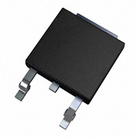
DPAK CASE 369C STYLE 1
1
3 DPAK CASE 369D STYLE 1
TYPICAL GAIN
Typical Gain @ IC = 1 A, VCE = 2 V Typical Gain @ IC = 0.3 A, VCE = 1 V hFE hFE 13 16 − −
Stresses exceeding Maximum Ratings may damage the device. Maximum Ratings are stress ratings only. Functional operation above the Recommended Operating Conditions is not implied. Extended exposure to stresses above the Recommended Operating Conditions may affect device reliability. 1. Pulse Test: Pulse Width = 5.0 ms, Duty Cycle = 10%10
ORDERING INFORMATION
See detailed ordering and shipping information in the package dimensions section on page 10 of this data sheet.
© Semiconductor Components Industries, LLC, 2011
1
January, 2011 − Rev. 5
�ÎÎ Î Î ÎÎÎÎÎÎÎÎÎÎ ÎÎÎÎÎÎÎÎ Î ÎÎ ÎÎ Î ÎÎ Î ÎÎÎÎÎÎÎÎÎÎÎÎÎÎ ÎÎÎÎÎÎÎÎÎÎÎÎÎÎÎÎÎÎ ÎÎ ÎÎÎÎÎÎÎÎÎÎ ÎÎÎÎÎÎÎÎÎÎÎÎÎÎÎÎÎÎÎÎÎ Î Î Î Î ÎÎÎÎ ÎÎ ÎÎÎÎÎÎÎÎÎÎ ÎÎÎÎÎÎÎÎÎÎÎÎÎÎÎÎÎÎÎÎÎ Î ÎÎ ÎÎ Î ÎÎ Î ÎÎÎÎÎÎÎÎÎÎÎÎÎÎÎÎÎÎ ÎÎ ÎÎÎÎÎÎÎÎÎÎ ÎÎÎÎÎÎÎÎÎÎÎÎÎÎ Î Î Î Î ÎÎÎÎ Î ÎÎÎÎÎÎÎÎÎÎÎÎÎÎ ÎÎÎÎÎÎÎÎÎÎ ÎÎÎÎÎÎÎÎ Î Î Î Î ÎÎÎÎ Î ÎÎ Î Î ÎÎÎÎÎÎÎÎÎÎÎÎÎÎ ÎÎÎÎÎÎÎÎÎÎÎÎÎÎÎÎÎÎÎÎÎÎÎÎÎÎÎÎÎÎÎÎÎ ÎÎÎÎÎÎÎÎ ÎÎÎÎÎÎÎÎ ÎÎ Î ÎÎÎÎÎÎÎÎÎÎÎÎÎÎÎÎÎÎÎÎÎÎÎÎÎÎÎÎÎÎÎÎÎ ÎÎ Î ÎÎÎ Î Î Î Î ÎÎ ÎÎ ÎÎÎÎÎÎÎÎÎÎÎÎÎÎÎÎÎÎÎÎÎÎÎÎÎÎÎÎÎÎÎÎÎ Î Î Î Î Î Î Î Î Î Î Î ÎÎÎÎÎÎÎÎÎÎÎÎÎÎÎÎÎÎÎÎ ÎÎÎÎÎÎÎÎÎÎÎÎÎÎÎÎÎÎÎÎÎÎÎÎÎÎÎÎÎÎÎÎÎ Î ÎÎÎÎÎÎÎÎÎÎÎÎÎÎÎÎÎÎÎÎÎÎÎÎÎÎÎÎÎÎÎÎÎ ÎÎ ÎÎ Î ÎÎÎÎÎÎÎÎÎÎÎÎÎÎÎÎÎÎÎÎÎÎÎÎÎÎÎÎÎÎÎÎÎ ÎÎ ÎÎ Î ÎÎÎÎÎÎÎÎÎÎÎÎÎÎÎÎÎÎÎÎÎÎÎÎÎÎÎÎÎÎÎÎÎ ÎÎ ÎÎ Î ÎÎÎÎÎÎÎÎÎÎÎÎÎÎÎÎÎÎÎÎÎÎÎÎÎÎÎÎÎÎÎÎÎ ÎÎ ÎÎ Î ÎÎÎÎÎÎÎÎÎÎÎÎÎÎÎÎÎÎÎÎÎÎÎÎÎÎÎÎÎÎÎÎÎ ÎÎÎÎÎÎÎÎÎÎÎÎÎÎÎÎÎÎÎÎÎÎÎÎÎÎÎÎÎÎÎÎÎ ÎÎ ÎÎ Î ÎÎÎÎÎÎÎÎÎÎÎÎÎÎÎÎÎÎÎÎÎÎÎÎÎÎÎÎÎÎÎÎÎ ÎÎ ÎÎ Î ÎÎÎÎÎÎÎÎÎÎÎÎÎÎÎÎÎÎÎÎÎÎÎÎÎÎÎÎÎÎÎÎÎ ÎÎÎÎÎÎÎÎÎÎÎÎÎÎÎÎÎÎÎÎÎÎÎÎÎÎÎÎÎÎÎÎÎ ÎÎÎÎÎÎÎÎÎÎÎÎÎÎÎÎÎÎÎÎÎÎÎÎÎÎÎÎÎÎÎÎÎ ÎÎ ÎÎ Î ÎÎÎÎÎÎÎÎÎÎÎÎÎÎÎÎÎÎÎÎÎÎÎÎÎÎÎÎÎÎÎÎÎ ÎÎ ÎÎ Î ÎÎÎÎÎÎÎÎÎÎÎÎÎÎÎÎÎÎÎÎÎÎÎÎÎÎÎÎÎÎÎÎÎ ÎÎÎÎÎÎÎÎÎÎÎÎÎÎÎÎÎÎÎÎÎÎÎÎÎÎÎÎÎÎÎÎÎ ÎÎ ÎÎ Î ÎÎÎÎÎÎÎÎÎÎÎÎÎÎÎÎÎÎÎÎÎÎÎÎÎÎÎÎÎÎÎÎÎ ÎÎ ÎÎ Î ÎÎÎÎÎÎÎÎÎÎÎÎÎÎÎÎÎÎÎÎÎÎÎÎÎÎÎÎÎÎÎÎÎ ÎÎ ÎÎ Î ÎÎÎÎÎÎÎÎÎÎÎÎÎÎÎÎÎÎÎÎÎÎÎÎÎÎÎÎÎÎÎÎÎ ÎÎ ÎÎ Î ÎÎÎÎÎÎÎÎÎÎÎÎÎÎÎÎÎÎÎÎÎÎÎÎÎÎÎÎÎÎÎÎÎ ÎÎ ÎÎ Î ÎÎÎÎÎÎÎÎÎÎÎÎÎÎÎÎÎÎÎÎÎÎÎÎÎÎÎÎÎÎÎÎÎ ÎÎ ÎÎ Î ÎÎÎÎÎÎÎÎÎÎÎÎÎÎÎÎÎÎÎÎÎÎÎÎÎÎÎÎÎÎÎÎÎ ÎÎ ÎÎ Î ÎÎÎÎÎÎÎÎÎÎÎÎÎÎÎÎÎÎÎÎÎÎÎÎÎÎÎÎÎÎÎÎÎ ÎÎÎÎÎÎÎÎÎÎÎÎÎÎÎÎÎÎÎÎÎÎÎÎÎÎÎÎÎÎÎÎÎ ÎÎ ÎÎ Î ÎÎÎÎÎÎÎÎÎÎÎÎÎÎÎÎÎÎÎÎÎÎÎÎÎÎÎÎÎÎÎÎÎ ÎÎ ÎÎ Î ÎÎÎÎÎÎÎÎÎÎÎÎÎÎÎÎÎÎÎÎÎÎÎÎÎÎÎÎÎÎÎÎÎ ÎÎÎÎÎÎÎÎÎÎÎÎÎÎÎÎÎÎÎÎÎÎÎÎÎÎÎÎÎÎÎÎÎ ÎÎ ÎÎ Î Î ÎÎÎÎÎÎÎÎÎÎÎÎÎÎÎÎÎÎÎÎÎÎÎÎÎÎÎÎÎÎÎÎÎ ÎÎ ÎÎ Î ÎÎÎÎÎÎÎÎÎÎÎÎÎÎÎÎÎÎÎÎÎÎÎÎÎÎÎÎÎÎÎÎÎ ÎÎ ÎÎ Î Î ÎÎÎÎÎÎÎÎÎÎÎÎÎÎÎÎÎÎÎÎÎÎÎÎÎÎÎÎÎÎÎÎÎ ÎÎ ÎÎ Î Î ÎÎÎÎÎÎÎÎÎÎÎÎÎÎÎÎÎÎÎÎÎÎÎÎÎÎÎÎÎÎÎÎÎ ÎÎ ÎÎ Î Î ÎÎÎÎÎÎÎÎÎÎÎÎÎÎÎÎÎÎÎÎÎÎÎÎÎÎÎÎÎÎÎÎÎ ÎÎ ÎÎ Î Î ÎÎÎÎÎÎÎÎÎÎÎÎÎÎÎÎÎÎÎÎÎÎÎÎÎÎÎÎÎÎÎÎÎ ÎÎ ÎÎ Î Î ÎÎÎÎÎÎÎÎÎÎÎÎÎÎÎÎÎÎÎÎÎÎÎÎÎÎÎÎÎÎÎÎÎ ÎÎ ÎÎ Î ÎÎÎ Î Î Î Î Î ÎÎÎÎÎÎÎÎÎÎÎÎÎÎÎÎÎÎÎÎÎÎÎÎÎÎÎÎÎÎÎÎÎ ÎÎ ÎÎ Î ÎÎÎÎÎÎÎÎÎÎÎÎÎÎÎÎÎÎÎÎÎÎÎÎÎÎÎÎÎÎÎÎÎ ÎÎÎÎÎÎÎÎÎÎÎÎÎÎÎÎÎÎÎÎÎÎÎÎÎÎÎÎÎÎÎ Î ÎÎ Î ÎÎÎ Î Î Î Î Î ÎÎÎÎÎÎÎÎÎÎÎÎÎÎÎÎÎÎÎÎÎÎÎÎÎÎÎÎÎÎÎÎÎ ÎÎ ÎÎ Î ÎÎÎÎÎÎÎÎÎÎÎÎÎÎÎÎÎÎÎÎÎÎÎÎÎÎÎÎÎÎÎÎÎ ÎÎÎÎÎÎÎÎÎÎÎÎÎÎÎÎÎÎÎÎÎÎÎÎÎÎÎÎÎÎÎ Î ÎÎ Î ÎÎÎÎÎÎÎÎÎÎÎÎÎÎÎÎÎÎÎÎÎÎÎÎÎÎÎÎÎÎÎÎÎ ÎÎÎÎÎÎÎÎÎÎÎÎÎÎÎÎÎÎÎÎÎÎÎÎÎÎÎÎÎÎÎÎÎ ÎÎ ÎÎ Î ÎÎÎ Î Î Î Î Î ÎÎÎÎÎÎÎÎÎÎÎÎÎÎÎÎÎÎÎÎÎÎÎÎÎÎÎÎÎÎÎÎÎ ÎÎÎÎÎÎÎÎÎÎÎÎÎÎÎÎÎÎÎÎÎÎÎÎÎÎÎÎÎÎÎÎÎ ÎÎÎÎÎÎÎÎÎÎÎÎÎÎÎÎÎÎÎÎÎÎÎÎÎÎÎÎÎÎÎ Î ÎÎ Î
ELECTRICAL CHARACTERISTICS (TC = 25°C unless otherwise noted) THERMAL CHARACTERISTICS
DYNAMIC SATURATION VOLTAGE SWITCHING CHARACTERISTICS: Resistive Load (D.C.≤ 10%, Pulse Width = 40 ms) DIODE CHARACTERISTICS ON CHARACTERISTICS OFF CHARACTERISTICS Maximum Lead Temperature for Soldering Purposes: 1/8 in from Case for 5 seconds Thermal Resistance, Junction−to−Ambient Thermal Resistance, Junction−to−Case Dynamic Saturation Voltage: Determined 1 ms and 3 ms respectively after rising IB1 reaches 90% of final IB1 Collector Cutoff Current (VCE = Rated VCES, VEB = 0) Fall Time (IC = 2.5 Adc, IB1 = IB2 = 0.5 A, VCC = 150 V, VBE = −2 V) Turn−Off Time (IC = 1.2 Adc, IB1 = 0.4 A, IB2 = 0.1 A, VCC = 300 V) Forward Diode Voltage (IEC = 1.0 Adc) DC Current Gain (IC = 1 Adc, VCE = 2 Vdc) (IC = 2 Adc, VCE = 5 Vdc) Collector−Emitter Saturation Voltage (IC = 2 Adc, IB = 0.5 Adc) Base−Emitter Saturation Voltage (IC = 1 Adc, IB = 0.2 Adc) Emitter−Cutoff Current (VEB = 9 Vdc, IC = 0) Collector Cutoff Current (VCE = Rated VCEO, IB = 0) Emitter−Base Breakdown Voltage (IEBO = 1 mA) Collector−Base Breakdown Voltage (ICBO = 1 mA) Collector−Emitter Sustaining Voltage (IC = 100 mA, L = 25 mH) Characteristic Characteristic IC = 1 A IB1 = 200 mA VCC = 300 V IC = 400 mA IB1 = 40 mA VCC = 300 V @ 3 ms @ 1 ms @ 3 ms @ 1 ms @ TC = 25°C @ TC = 125°C @ TC = 25°C @ TC = 125°C @ TC = 25°C @ TC = 125°C @ TC = 25°C @ TC = 125°C @ TC = 25°C @ TC = 125°C @ TC = 25°C @ TC = 125°C VCEO(sus) VCE(dsat) Symbol Symbol VCE(sat) VBE(sat) VCBO VEBO RqJC RqJA ICEO IEBO ICES VEC hFE Toff TL Tf Min 650 350 4.6 8.0 10 9.0 − − − − − − − − − − − − − − − − − Value 0.35 0.6 0.75 1.3 0.85 71.4 Typ 780 430 260 2.1 4.7 2.8 3.2 0.9 0.2 5.0 13 12 12 − − − − − − − 6.55 Max 10 200 100 100 200 0.8 1.5 1.0 1.2 − − − − − − − − − − − − − °C/W °C/W mAdc mAdc mAdc Unit Unit Vdc Vdc Vdc Vdc Vdc °C ms ms V V −
http://onsemi.com
BUD42D
2
�BUD42D
TYPICAL STATIC CHARACTERISTICS
100 100
hFE , DC CURRENT GAIN
hFE , DC CURRENT GAIN
TJ = 125°C TJ = 25°C 10 TJ = - 20°C
TJ = 125°C TJ = 25°C 10 TJ = - 20°C
1 0.001 0.01 0.1 1 IC, COLLECTOR CURRENT (AMPS) 10
1 0.001 0.01 0.1 1 IC, COLLECTOR CURRENT (AMPS) 10
Figure 1. DC Current Gain @ VCE = 1 V
Figure 2. DC Current Gain @ VCE = 5 V
3 TJ = 25°C VCE , VOLTAGE (VOLTS) VCE , VOLTAGE (VOLTS)
10 IC/IB = 5
2A 2 1.5 A 1A 1 0.4 A
1
TJ = 125°C 0.1 TJ = - 20°C
TJ = 25°C
IC = 0.2 A 0 0.001 0.01
0.1 1 IB, BASE CURRENT (AMPS)
10
0.01 0.001
0.01 0.1 1 IC, COLLECTOR CURRENT (AMPS)
10
Figure 3. Collector Saturation Region
Figure 4. Collector−Emitter Saturation Voltage
100 IC/IB = 8 VCE , VOLTAGE (VOLTS) VCE , VOLTAGE (VOLTS) 10 TJ = 125°C 1 TJ = - 20°C
10 IC/IB = 10 TJ = - 20°C TJ = 125°C TJ = 25°C
1
TJ = 25°C
0.1
0.1
0.01 0.001
1 0.01 0.1 IC, COLLECTOR CURRENT (AMPS)
10
0.01 0.001
1 0.01 0.1 IC, COLLECTOR CURRENT (AMPS)
10
Figure 5. Collector−Emitter Saturation Voltage
Figure 6. Collector−Emitter Saturation Voltage
http://onsemi.com
3
�BUD42D
TYPICAL STATIC CHARACTERISTICS
10 IC/IB = 5 VBE , VOLTAGE (VOLTS) VBE , VOLTAGE (VOLTS) 10 IC/IB = 8
1
TJ = - 20°C
1
TJ = - 20°C
TJ = 125°C
TJ = 25°C
TJ = 125°C
TJ = 25°C
0.1 0.001
1 0.01 0.1 IC, COLLECTOR CURRENT (AMPS)
10
0.1 0.001
1 0.01 0.1 IC, COLLECTOR CURRENT (AMPS)
10
Figure 7. Base−Emitter Saturation Region
Figure 8. Base−Emitter Saturation Region
10 FORWARD DIODE VOLTAGE (VOLTS) IC/IB = 10 VBE , VOLTAGE (VOLTS)
10
1
TJ = - 20°C
1
VEC(V) = - 20°C VEC(V) = 125°C VEC(V) = 25°C
TJ = 125°C
TJ = 25°C
0.1 0.001
0.01 0.1 1 IC, COLLECTOR CURRENT (AMPS)
10
0.1 0.01
0.1 1 REVERSE EMITTER-COLLECTOR CURRENT
10
Figure 9. Base−Emitter Saturation Region
Figure 10. Forward Diode Voltage
http://onsemi.com
4
�BUD42D
TYPICAL SWITCHING CHARACTERISTICS
1000 Cib C, CAPACITANCE (pF) TJ = 25°C f(test) = 1 MHz BVCER (VOLTS) 900 800 700 600 500 400 TC = 25°C 1 1 10 VR, REVERSE VOLTAGE (VOLTS) 100 300 10 100 RBE (W) 1000 10000 ICER = 100 mA lC = 25 mH ICER = 10 mA
100 Cob 10
Figure 11. Capacitance
Figure 12. BVCER = f(RBE)
800 700 600 t, TIME (ns) 500 400 300 200 100 0 0 1 0.5 1.5 IC, COLLECTOR CURRENT (AMPS) 2 TJ = 125°C TJ = 25°C hFE = 5 hFE = 10 IBon = IBoff VCC = 300 V PW = 40 ms
9 IBon = IBoff VCC = 300 V PW = 40 ms 6 t, TIME (ns)
hFE = 5 3 TJ = 125°C TJ = 25°C 0 0
hFE = 10 2
0.5 1 1.5 IC, COLLECTOR CURRENT (AMPS)
Figure 13. Resistive Switching, ton
Figure 14. Resistive Switching, toff
4 IBon = IBoff VCE = 15 V VZ = 300 V LC = 200 mH TJ = 125°C
4 IBon = IBoff VCE = 15 V VZ = 300 V LC = 200 mH
3 t, TIME ( μ s)
TJ = 125°C 3 TJ = 25°C t, TIME ( μ s) TJ = 25°C 2
2
1
0 0 0.5 1 1.5 IC, COLLECTOR CURRENT (AMPS) 2
1 0.5 1.5 1 IC, COLLECTOR CURRENT (AMPS) 2
Figure 15. Inductive Storage Time, tsi @ hFE = 5 http://onsemi.com
5
Figure 16. Inductive Storage Time, tsi @ hFE = 10
�BUD42D
TYPICAL SWITCHING CHARACTERISTICS
400 IBon = IBoff VCC = 15 V VZ = 300 V LC = 200 mH 300 t, TIME (ns) tc 200 tfi t, TIME (ns) TJ = 125°C TJ = 25°C 200 TJ = 125°C 250
TJ = 25°C 150 IBon = IBoff VCE = 15 V VZ = 300 V LC = 200 mH 0.5 1 1.5 IC, COLLECTOR CURRENT (AMPS) 2
100
100 0 0.5 1.5 1 IC, COLLECTOR CURRENT (AMPS) 2
Figure 17. Inductive Fall and Cross Over Time, tfi and tc @ hFE = 5
500 IBon = IBoff VCC = 15 V VZ = 300 V LC = 200 mH TJ = 125°C 4 t, TIME ( m s) 5
Figure 18. Inductive Fall Time, tfi @ hFE = 10
IBon = IBoff VCC = 15 V VZ = 300 V LC = 200 mH IC = 1 A
TJ = 125°C TJ = 25°C
400 t, TIME (ns)
3
300 TJ = 25°C 2 IC = 0.3 A
200 0.5 1 1.5 IC, COLLECTOR CURRENT (AMPS) 2
1 3 4 5 6 7 8 9 hFE, FORCED GAIN 10 11 12
Figure 19. Inductive Cross Over Time, tc @ hFE = 10
Figure 20. Inductive Storage Time, tsi
300 IBon = IBoff VCC = 15 V VZ = 300 V LC = 200 mH
300
CROSS-OVER TIME (ns)
IC = 0.3 A
IC = 0.3 A IC = 1 A 200
t fi , FALL TIME (ns)
200 IC = 1 A
TJ = 125°C TJ = 25°C 100 3 4 5 6 7 hFE, FORCED GAIN 8 9 10 100 2 4
TJ = 125°C TJ = 25°C 6 hFE, FORCED GAIN 8
IBon = IBoff VCC = 15 V VZ = 300 V LC = 200 mH 10
Figure 21. Inductive Fall Time, tf http://onsemi.com
6
Figure 22. Inductive Cross Over Time, tc
�BUD42D
TYPICAL SWITCHING CHARACTERISTICS
3 IBon = IBoff VCC = 15 V VZ = 300 V LC = 200 mH IB 1 & 2 = 200 mA t fr , FORWARD RECOVERY TIME (ns) 440 420 400 380 360 340 320 300 0 0.5 1.5 1 IC, COLLECTOR CURRENT (AMPS) 2 0 1 0.5 1.5 IF, FORWARD CURRENT (AMPS) 2 di/dt = 10 A/ms, TC = 25°C
2.5 t, TIME ( m s)
500 mA
2 50 mA 100 mA
1.5
1
Figure 23. Inductive Storage Time, tsi
Figure 24. Forward Recovery Time, tfr
10 VCE Dyn 1 ms Dyn 3 ms 6 0V Vclamp 90% IB IB 1 ms 3 ms 2 0 0 TIME 2 4 TIME 6 8 4 IB 90% IB1 tc 10% Vclamp 8 IC 90% IC tsi tfi 10% IC
Figure 25. Dynamic Saturation Voltage Measurements
Figure 26. Inductive Switching Measurements
http://onsemi.com
7
�BUD42D
TYPICAL SWITCHING CHARACTERISTICS
Table 1. Inductive Load Switching Drive Circuit
+15 V 1 mF 150 W 3W 100 W 3W MTP8P10 100 mF VCE PEAK MTP8P10 MPF930 MUR105 +10 V MPF930 A 50 W 500 mF 150 W 3W RB2 MTP12N10 V(BR)CEO(sus) L = 10 mH RB2 = ∞ VCC = 20 Volts IC(pk) = 100 mA IB2 Inductive Switching L = 200 mH RB2 = 0 VCC = 15 Volts RB1 selected for desired IB1 RBSOA L = 500 mH RB2 = 0 VCC = 15 Volts RB1 selected for desired IB1 Iout IB RB1 VCE IB1 IC PEAK
MJE210
COMMON
1 mF -Voff
VFRM VF
VFR (1.1 VF) UNLESS OTHERWISE SPECIFIED
0.1 VF
tfr
IF
10% IF
Figure 27. tfr Measurement
http://onsemi.com
8
�BUD42D
MAXIMUM RATINGS
10 IC , COLLECTOR CURRENT (AMPS) IC , COLLECTOR CURRENT (AMPS) 5 ms dc 1 EXTENDED SOA 1 ms 10 ms 1 ms 4 5 TJ = 125°C GAIN ≥ 4 LC = 500 mH
3
2 VBE(off) = -5 V VBE = 0 V 300 VBE(off) = -1.5 V 700
0.1
1 0
0.01 10 100 VCE, COLLECTOR-EMITTER VOLTAGE (VOLTS) 1000
400 500 600 VCE, COLLECTOR-EMITTER VOLTAGE (VOLTS)
Figure 28. Forward Bias Safe Operating Area
Figure 29. Reverse Bias Safe Operating Area
1 SECOND BREAKDOWN DERATING
POWER DERATING FACTOR
0.8
0.6
0.4
0.2 THERMAL DERATING 0 20 40 60 80 100 120 TC, CASE TEMPERATURE (°C) 140 160
Figure 30. Power Derating
There are two limitations on the power handling ability of a transistor: average junction temperature and second breakdown. Safe operating area curves indicate IC−VCE limits of the transistor that must be observed for reliable operation; i.e., the transistor must not be subjected to greater dissipation than the curves indicate. The data of Figure 28 is based on TC = 25°C; Tj(pk) is variable depending on power level. Second breakdown pulse limits are valid for duty cycles to 10% but must be derated when TC > 25°C. Second Breakdown limitations do not derate like thermal limitations. Allowable current at the voltages shown on
Figure 28 may be found at any case temperature by using the appropriate curve on Figure 30. Tj(pk) may be calculated from the data in Figure 31. At any case temperatures, thermal limitations will reduce the power that can be handled to values less than the limitations imposed by second breakdown. For inductive loads, high voltage and current must be sustained simultaneously during turn−off with the base to emitter junction reverse biased. The safe level is specified as reverse biased safe operating area (Figure 29). This rating is verified under clamped conditions so that the device is never subjected to an avalanche mode.
http://onsemi.com
9
�BUD42D
1 D = 0.5 r(t) TRANSIENT THERMAL RESISTANCE (NORMALIZED)
0.2 0.1 0.1 0.05 0.02 0.01 t1 SINGLE PULSE 0.01 0.01 0.1 1 t, TIME (ms) 10 100 1000 t2 DUTY CYCLE, D = t1/t2 P(pk) RqJC(t) = r(t) RqJC RqJC = 5°C/W MAX D CURVES APPLY FOR POWER PULSE TRAIN SHOWN READ TIME AT t1 TJ(pk) - TC = P(pk) RqJC(t)
Figure 31. Thermal Response
ORDERING INFORMATION
Device BUD42D−1G Package DPAK Straight Lead (Pb−Free) DPAK (Pb−Free) Shipping† 75 Units / Rail
BUD42DT4G
2500 Units / Tape & Reel
†For information on tape and reel specifications, including part orientation and tape sizes, please refer to our Tape and Reel Packaging Specifications Brochure, BRD8011/D.
http://onsemi.com
10
�BUD42D
PACKAGE DIMENSIONS
DPAK CASE 369C−01 ISSUE D
A B C A c2
NOTES: 1. DIMENSIONING AND TOLERANCING PER ASME Y14.5M, 1994. 2. CONTROLLING DIMENSION: INCHES. 3. THERMAL PAD CONTOUR OPTIONAL WITHIN DIMENSIONS b3, L3 and Z. 4. DIMENSIONS D AND E DO NOT INCLUDE MOLD FLASH, PROTRUSIONS, OR BURRS. MOLD FLASH, PROTRUSIONS, OR GATE BURRS SHALL NOT EXCEED 0.006 INCHES PER SIDE. 5. DIMENSIONS D AND E ARE DETERMINED AT THE OUTERMOST EXTREMES OF THE PLASTIC BODY. 6. DATUMS A AND B ARE DETERMINED AT DATUM PLANE H. DIM A A1 b b2 b3 c c2 D E e H L L1 L2 L3 L4 Z INCHES MIN MAX 0.086 0.094 0.000 0.005 0.025 0.035 0.030 0.045 0.180 0.215 0.018 0.024 0.018 0.024 0.235 0.245 0.250 0.265 0.090 BSC 0.370 0.410 0.055 0.070 0.108 REF 0.020 BSC 0.035 0.050 −−− 0.040 0.155 −−− MILLIMETERS MIN MAX 2.18 2.38 0.00 0.13 0.63 0.89 0.76 1.14 4.57 5.46 0.46 0.61 0.46 0.61 5.97 6.22 6.35 6.73 2.29 BSC 9.40 10.41 1.40 1.78 2.74 REF 0.51 BSC 0.89 1.27 −−− 1.01 3.93 −−−
E b3 L3
1 4
D
2 3
Z
DETAIL A
H
L4
b2 e
b 0.005 (0.13)
M
c C L2
GAUGE PLANE
H C L L1 DETAIL A
SEATING PLANE
A1
ROTATED 90 CW 5
SOLDERING FOOTPRINT*
6.20 0.244 3.0 0.118
STYLE 1: PIN 1. BASE 2. COLLECTOR 3. EMITTER 4. COLLECTOR
2.58 0.101
5.80 0.228
1.6 0.063
6.172 0.243
SCALE 3:1
mm inches
*For additional information on our Pb−Free strategy and soldering details, please download the ON Semiconductor Soldering and Mounting Techniques Reference Manual, SOLDERRM/D.
http://onsemi.com
11
�BUD42D
PACKAGE DIMENSIONS
DPAK STRAIGHT LEAD CASE 369D−01 ISSUE B
B V R
4
C E Z
NOTES: 1. DIMENSIONING AND TOLERANCING PER ANSI Y14.5M, 1982. 2. CONTROLLING DIMENSION: INCH. DIM A B C D E F G H J K R S V Z INCHES MIN MAX 0.235 0.245 0.250 0.265 0.086 0.094 0.027 0.035 0.018 0.023 0.037 0.045 0.090 BSC 0.034 0.040 0.018 0.023 0.350 0.380 0.180 0.215 0.025 0.040 0.035 0.050 0.155 −−− MILLIMETERS MIN MAX 5.97 6.35 6.35 6.73 2.19 2.38 0.69 0.88 0.46 0.58 0.94 1.14 2.29 BSC 0.87 1.01 0.46 0.58 8.89 9.65 4.45 5.45 0.63 1.01 0.89 1.27 3.93 −−−
S −T−
SEATING PLANE
A
1 2 3
K
F D G
3 PL
J
H
M
0.13 (0.005)
T
STYLE 1: PIN 1. BASE 2. COLLECTOR 3. EMITTER 4. COLLECTOR
ON Semiconductor and are registered trademarks of Semiconductor Components Industries, LLC (SCILLC). SCILLC reserves the right to make changes without further notice to any products herein. SCILLC makes no warranty, representation or guarantee regarding the suitability of its products for any particular purpose, nor does SCILLC assume any liability arising out of the application or use of any product or circuit, and specifically disclaims any and all liability, including without limitation special, consequential or incidental damages. “Typical” parameters which may be provided in SCILLC data sheets and/or specifications can and do vary in different applications and actual performance may vary over time. All operating parameters, including “Typicals” must be validated for each customer application by customer’s technical experts. SCILLC does not convey any license under its patent rights nor the rights of others. SCILLC products are not designed, intended, or authorized for use as components in systems intended for surgical implant into the body, or other applications intended to support or sustain life, or for any other application in which the failure of the SCILLC product could create a situation where personal injury or death may occur. Should Buyer purchase or use SCILLC products for any such unintended or unauthorized application, Buyer shall indemnify and hold SCILLC and its officers, employees, subsidiaries, affiliates, and distributors harmless against all claims, costs, damages, and expenses, and reasonable attorney fees arising out of, directly or indirectly, any claim of personal injury or death associated with such unintended or unauthorized use, even if such claim alleges that SCILLC was negligent regarding the design or manufacture of the part. SCILLC is an Equal Opportunity/Affirmative Action Employer. This literature is subject to all applicable copyright laws and is not for resale in any manner.
PUBLICATION ORDERING INFORMATION
LITERATURE FULFILLMENT: Literature Distribution Center for ON Semiconductor P.O. Box 5163, Denver, Colorado 80217 USA Phone: 303−675−2175 or 800−344−3860 Toll Free USA/Canada Fax: 303−675−2176 or 800−344−3867 Toll Free USA/Canada Email: orderlit@onsemi.com N. American Technical Support: 800−282−9855 Toll Free USA/Canada Europe, Middle East and Africa Technical Support: Phone: 421 33 790 2910 Japan Customer Focus Center Phone: 81−3−5773−3850 ON Semiconductor Website: www.onsemi.com Order Literature: http://www.onsemi.com/orderlit For additional information, please contact your local Sales Representative
http://onsemi.com
12
BUD42D/D
�