BUV21
SWITCHMODEt Series
NPN Silicon Power
Transistor
This device is designed for high speed, high current, high power
applications.
Features
http://onsemi.com
40 AMPERES
NPN SILICON POWER
METAL TRANSISTOR
200 VOLTS − 250 WATTS
• High DC Current Gain:
hFE min = 20 at IC = 12 A
• Low VCE(sat), VCE(sat)
max = 0.6 V at IC = 8 A
• Very Fast Switching Times:
•
NPN
TF max = 0.4 ms at IC = 25 A
These are Pb−Free Devices*
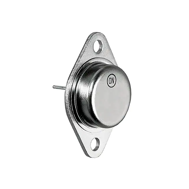
COLLECTOR
CASE
MAXIMUM RATINGS
Rating
Symbol
Value
Unit
VCEO(SUS)
200
Vdc
Collector−Base Voltage
VCBO
250
Vdc
Emitter−Base Voltage
VEBO
7
Vdc
Collector−Emitter Voltage (VBE = −1.5 V)
VCEX
250
Vdc
Collector−Emitter Voltage (RBE = 100 W)
VCER
240
Vdc
Collector−Current − Continuous
− Peak (PW v 10 ms)
IC
ICM
40
50
Adc
Apk
Base−Current Continuous
IB
8
Adc
Total Device Dissipation @ TC = 25_C
PD
250
W
TJ, Tstg
−65 to 200
_C
Collector−Emitter Voltage
Operating and Storage Junction
Temperature Range
THERMAL CHARACTERISTICS
Characteristics
Thermal Resistance, Junction−to−Case
Symbol
Max
Unit
qJC
0.7
_C/W
BASE
1
EMITTER 2
MARKING
DIAGRAM
2
BUV21G
AYWW
MEX
1
TO−204AE (TO−3)
CASE 197A
STYLE 1
BUV21
G
A
Y
WW
MEX
Stresses exceeding those listed in the Maximum Ratings table may damage the
device. If any of these limits are exceeded, device functionality should not be
assumed, damage may occur and reliability may be affected.
= Device Code
= Pb−Free Package
= Assembly Location
= Year
= Work Week
= Country of Origin
ORDERING INFORMATION
Device
Package
Shipping
BUV21G
TO−204
(Pb−Free)
100 Units / Tray
*For additional information on our Pb−Free strategy and soldering details, please
download the ON Semiconductor Soldering and Mounting Techniques
Reference Manual, SOLDERRM/D.
© Semiconductor Components Industries, LLC, 2013
December, 2013 − Rev. 11
1
Publication Order Number:
BUV21/D
�BUV21
ÎÎÎÎÎÎÎÎÎÎÎÎÎÎÎÎÎÎÎÎÎÎÎÎÎÎÎÎÎÎÎÎÎ
ÎÎÎÎÎÎÎÎÎÎÎÎÎÎÎÎÎÎÎÎÎÎÎÎÎÎÎÎÎÎÎÎÎ
ÎÎÎÎÎÎÎÎÎÎÎÎÎÎÎÎÎÎÎÎÎÎ
ÎÎÎÎÎÎÎÎÎÎÎÎÎÎÎ
ÎÎÎÎÎÎÎÎÎÎÎÎÎÎÎÎÎÎÎÎÎÎÎÎÎÎÎÎÎÎÎÎÎÎÎÎÎ
ÎÎÎÎÎÎÎÎÎÎÎÎÎÎÎÎÎÎÎÎÎÎÎÎÎÎÎÎÎÎÎÎÎ
ÎÎÎÎÎÎÎÎÎÎÎÎÎÎÎÎÎÎÎÎÎÎÎÎÎÎÎÎÎÎÎÎÎ
ÎÎÎÎÎÎÎÎÎÎÎÎÎÎÎÎÎÎÎÎÎÎ
ÎÎÎÎÎÎÎÎÎÎÎÎÎÎÎ
ÎÎÎÎÎÎÎÎÎÎÎÎÎÎÎÎÎÎÎÎÎÎÎÎÎÎÎÎÎÎÎÎÎÎÎÎÎ
ÎÎÎÎÎÎÎÎÎÎÎÎÎÎÎÎÎÎÎÎÎÎÎÎÎÎÎÎÎÎÎÎÎÎÎÎÎ
ÎÎÎÎÎÎÎÎÎÎÎÎÎÎÎÎÎÎÎÎÎÎÎÎÎÎÎÎÎÎÎÎÎÎÎÎÎ
ÎÎÎÎÎÎÎÎÎÎÎÎÎÎÎÎÎÎÎÎÎÎÎÎÎÎÎÎÎÎÎÎÎÎÎÎÎ
ÎÎÎÎÎÎÎÎÎÎÎÎÎÎÎÎÎÎÎÎÎÎÎÎÎÎÎÎÎÎÎÎÎÎÎÎÎ
ÎÎÎÎÎÎÎÎÎÎÎÎÎÎÎÎÎÎÎÎÎÎÎÎÎÎÎÎÎÎÎÎÎÎÎÎÎ
ÎÎÎÎÎÎÎÎÎÎÎÎÎÎÎÎÎÎÎÎÎÎ
ÎÎÎÎÎ
ÎÎÎ
ÎÎÎÎ
ÎÎÎ
ÎÎÎÎÎÎÎÎÎÎÎÎÎÎÎÎÎÎÎÎÎÎÎÎÎÎÎÎÎÎÎÎÎÎÎÎÎ
ÎÎÎÎÎÎÎÎÎÎÎÎÎÎÎÎÎÎÎÎÎÎÎÎÎÎÎÎÎÎÎÎÎÎÎÎÎ
ÎÎÎÎÎÎÎÎÎÎÎÎÎÎÎÎÎÎÎÎÎÎÎÎÎÎÎÎÎÎÎÎÎ
ÎÎÎÎÎÎÎÎÎÎÎÎÎÎÎÎÎÎÎÎÎÎÎÎÎÎÎÎÎÎÎÎÎ
ÎÎÎÎÎÎÎÎÎÎÎÎÎÎÎÎÎÎÎÎÎÎ
ÎÎÎÎÎÎÎÎÎÎÎÎÎÎÎ
ÎÎÎÎÎÎÎÎÎÎÎÎÎÎÎÎÎÎÎÎÎÎÎÎÎÎÎÎÎÎÎÎÎÎÎÎÎ
ÎÎÎÎÎÎÎÎÎÎÎÎÎÎÎÎÎÎÎÎÎÎÎÎÎÎÎÎÎÎÎÎÎÎÎÎÎ
ÎÎÎÎÎÎÎÎÎÎÎÎÎÎÎÎÎÎÎÎÎÎÎÎÎÎÎÎÎÎÎÎÎ
ÎÎÎÎÎÎÎÎÎÎÎÎÎÎÎÎÎÎÎÎÎÎÎÎÎÎÎÎÎÎÎÎÎ
ÎÎÎÎÎÎÎÎÎÎÎÎÎÎÎÎÎÎÎÎÎÎ
ÎÎÎÎÎÎÎÎÎÎÎÎÎÎÎ
ÎÎÎÎÎÎÎÎÎÎÎÎÎÎÎÎÎÎÎÎÎÎÎÎÎÎÎÎÎÎÎÎÎÎÎÎÎ
ÎÎÎÎÎÎÎÎÎÎÎÎÎÎÎÎÎÎÎÎÎÎÎÎÎÎÎÎÎÎÎÎÎÎÎÎÎ
ÎÎÎÎÎÎÎÎÎÎÎÎÎÎÎÎÎÎÎÎÎÎÎÎÎÎÎÎÎÎÎÎÎÎÎÎÎ
ÎÎÎÎÎÎÎÎÎÎÎÎÎÎÎÎÎÎÎÎÎÎÎÎÎÎÎÎÎÎÎÎÎÎÎÎÎ
ÎÎÎÎÎÎÎÎÎÎÎÎÎÎÎÎÎÎÎÎÎÎÎÎÎÎÎÎÎÎÎÎÎÎÎÎÎ
ÎÎÎÎÎÎÎÎÎÎÎÎÎÎÎÎÎÎÎÎÎÎ
ÎÎÎÎÎ
ÎÎÎ
ÎÎÎÎ
ÎÎÎ
ÎÎÎÎÎÎÎÎÎÎÎÎÎÎÎÎÎÎÎÎÎÎÎÎÎÎÎÎÎÎÎÎÎÎÎÎÎ
ÎÎÎÎÎÎÎÎÎÎÎÎÎÎÎÎÎÎÎÎÎÎÎÎÎÎÎÎÎÎÎÎÎ
ÎÎÎÎÎÎÎÎÎÎÎÎÎÎÎÎÎÎÎÎÎÎÎÎÎÎÎÎÎÎÎÎÎ
ÎÎÎÎÎÎÎÎÎÎÎÎÎÎÎÎÎÎÎÎÎÎ
ÎÎÎÎÎÎÎÎÎÎÎÎÎÎÎ
ÎÎÎÎÎÎÎÎÎÎÎÎÎÎÎÎÎÎÎÎÎÎÎÎÎÎÎÎÎÎÎÎÎÎÎÎÎ
ÎÎÎÎÎÎÎÎÎÎÎÎÎÎÎÎÎÎÎÎÎÎÎÎÎÎÎÎÎÎÎÎÎ
ÎÎÎÎÎÎÎÎÎÎÎÎÎÎÎÎÎÎÎÎÎÎÎÎÎÎÎÎÎÎÎÎÎ
ÎÎÎÎÎÎÎÎÎ
ÎÎÎÎÎÎÎÎÎÎÎÎÎÎÎÎÎÎÎÎÎÎÎÎÎÎÎÎÎ
ÎÎÎÎÎÎÎÎÎÎÎÎÎÎÎÎÎÎÎÎÎÎÎ
ÎÎÎÎÎÎÎÎÎÎÎÎÎÎÎ
ÎÎÎ
ÎÎÎÎÎÎÎÎÎÎÎÎÎÎÎÎÎÎÎÎÎÎÎ
ÎÎÎÎÎ
ÎÎÎ
ÎÎÎÎ
ÎÎÎÎÎÎÎÎÎÎÎÎÎÎÎÎÎÎÎÎÎÎÎÎÎÎÎÎÎÎÎÎÎÎÎÎÎÎ
ELECTRICAL CHARACTERISTICS
Characteristic
Symbol
Min
VCEO(sus)
200
Max
Unit
OFF CHARACTERISTICS (Note 1)
Collector−Emitter Sustaining Voltage
(IC = 200 mA, IB = 0, L = 25 mH)
Collector Cutoff Current at Reverse Bias:
(VCE = 250 V, VBE = −1.5 V)(TC = 25_C unless otherwise noted)
(VCE = 250 V, VBE = −1.5 V, TC = 125_C)
ICEX
Collector−Emitter Cutoff Current
(VCE = 160 V)
ICEO
Emitter−Base Reverse Voltage
(IE = 50 mA)
VEBO
Emitter−Cutoff Current
(VEB = 5 V)
IEBO
Vdc
mAdc
3.0
12.0
3.0
7
mAdc
V
1.0
mAdc
SECOND BREAKDOWN
Second Breakdown Collector Current with base forward biased
(VCE = 20 V, t = 1 s)
(VCE = 140 V, t = 1 s)
IS/b
Adc
12
0.15
ON CHARACTERISTICS (Note 1)
DC Current Gain
(IC = 12 A, VCE = 2 V)
(IC = 25 A, VCE = 4 V)
hFE
20
10
Collector−Emitter Saturation Voltage
(IC = 12 A, IB = 1.2 A)
(IC = 25 A, IB = 3 A)
VCE(sat)
Base−Emitter Saturation Voltage
(IC = 25 A, IB = 3 A)
VBE(sat)
60
Vdc
0.6
1.5
1.5
Vdc
DYNAMIC CHARACTERISTICS
Current Gain − Bandwidth Product
(VCE = 15 V, IC = 2 A, f = 4 MHz)
fT
8.0
MHz
SWITCHING CHARACTERISTICS (Resistive Load)
Turn-on Time
(IC = 25 A, IB1 = IB2 = 3 A,
VCC = 100 V, RC = 4 W)
Storage Time
Fall Time
ton
1.0
ts
1.8
tf
0.4
ms
Product parametric performance is indicated in the Electrical Characteristics for the listed test conditions, unless otherwise noted. Product
performance may not be indicated by the Electrical Characteristics if operated under different conditions.
1. Pulse Test: Pulse Width v 300 ms, Duty Cycle v 2%.
1.0
DERATING FACTOR
0.8
0.6
0.4
0.2
0
40
80
120
TC, TEMPERATURE (°C)
Figure 1. Power Derating
http://onsemi.com
2
160
200
�BUV21
There are two limitations on the power handling ability of
a transistor: average junction temperature and second
breakdown. Safe operating area curves indicate IC − VCE
limits of the transistor that must be observed for reliable
operation i.e., the transistor must not be subjected to greater
dissipation than the curves indicate.
The data of Figure 2 is based on TC = 25_C, TJ(pk) is
variable depending on power level. Second breakdown
limitations do not derate the same as thermal limitations.
At high case temperatures, thermal limitations will reduce
the power that can be handled to values less than the
limitations imposed by second breakdown.
IC, COLLECTOR CURRENT (A)
40
10
1
0.1
1
10
100 200
VCE, COLLECTOR-EMITTER VOLTAGE (V)
Figure 2. Active Region Safe Operating Area
2.0
50
IC/IB = 8
VCE = 5 V
V, VOLTAGE (V)
1.6
40
1.2
30
VBE
0.8
20
0.4
10
VCE
0
1
0
100
10
1
IC, COLLECTOR CURRENT (A)
IC, COLLECTOR CURRENT (A)
Figure 3. “On” Voltages
Figure 4. DC Current Gain
VCE = 100 V
IC/IB1 = 8
IB1 = IB2
3.0
2.0
t, TIME (��s)
μ
10
VCC
10,000 mF
RC
1.0
IB2
tS
0.4
0.3
0.2
IB1
RB
ton
VCC = 100 V
RC = 4 W
RB = 2.2 W
tF
0
5
10
15
IC, COLLECTOR CURRENT (A)
RC − RB: Non inductive resistances
25
20
Figure 5. Resistive Switching Performance
Figure 6. Switching Times Test Circuit
SWITCHMODE is a trademark of Semiconductor Components Industries, LLC.
http://onsemi.com
3
�MECHANICAL CASE OUTLINE
PACKAGE DIMENSIONS
TO−204 (TO−3)
CASE 197A−05
ISSUE K
DATE 21 FEB 2000
SCALE 1:1
A
N
NOTES:
1. DIMENSIONING AND TOLERANCING PER
ANSI Y14.5M, 1982.
2. CONTROLLING DIMENSION: INCH.
C
E
D
−T−
U
DIM
A
B
C
D
E
G
H
K
L
N
Q
U
V
K
2 PL
0.30 (0.012)
V
SEATING
PLANE
T Q
M
M
Y
M
−Y−
L
2
G
H
B
INCHES
MIN
MAX
1.530 REF
0.990 1.050
0.250 0.335
0.057 0.063
0.060 0.070
0.430 BSC
0.215 BSC
0.440 0.480
0.665 BSC
0.760 0.830
0.151 0.165
1.187 BSC
0.131 0.188
MILLIMETERS
MIN MAX
38.86 REF
25.15 26.67
6.35
8.51
1.45
1.60
1.53
1.77
10.92 BSC
5.46 BSC
11.18 12.19
16.89 BSC
19.31 21.08
3.84
4.19
30.15 BSC
3.33
4.77
1
GENERIC
MARKING DIAGRAM*
−Q−
0.25 (0.010)
STYLE 1:
PIN 1. BASE
2. EMITTER
CASE: COLLECTOR
M
T Y
STYLE 2:
PIN 1. EMITTER
2. BASE
CASE: COLLECTOR
M
STYLE 3:
PIN 1. GATE
2. SOURCE
CASE: DRAIN
XXXXXX
A
YYWW
STYLE 4:
PIN 1. ANODE = 1
2. ANODE = 2
CASE: CATHODES
XXXXX
A
YY
WW
= Specific Device Code
= Assembly Locationa
= Year
= Work Week
*This information is generic. Please refer
to device data sheet for actual part
marking.
DOCUMENT NUMBER:
STATUS:
98ASB42128B
ON SEMICONDUCTOR STANDARD
NEW STANDARD:
© Semiconductor Components Industries, LLC, 2002
October, DESCRIPTION:
2002 − Rev. 0
TO−204 (TO−3)
http://onsemi.com
1
Electronic versions are uncontrolled except when
accessed directly from the Document Repository. Printed
versions are uncontrolled except when stamped
“CONTROLLED COPY” in red.
Case Outline Number:
PAGE 1 OFXXX
2
�DOCUMENT NUMBER:
98ASB42128B
PAGE 2 OF 2
ISSUE
K
REVISION
LEGALLY CHANGED TO ON
DATE
21 FEB 2000
ON Semiconductor and
are registered trademarks of Semiconductor Components Industries, LLC (SCILLC). SCILLC reserves the right to make
changes without further notice to any products herein. SCILLC makes no warranty, representation or guarantee regarding the suitability of its products for any
particular purpose, nor does SCILLC assume any liability arising out of the application or use of any product or circuit, and specifically disclaims any and all
liability, including without limitation special, consequential or incidental damages. “Typical” parameters which may be provided in SCILLC data sheets and/or
specifications can and do vary in different applications and actual performance may vary over time. All operating parameters, including “Typicals” must be
validated for each customer application by customer’s technical experts. SCILLC does not convey any license under its patent rights nor the rights of others.
SCILLC products are not designed, intended, or authorized for use as components in systems intended for surgical implant into the body, or other applications
intended to support or sustain life, or for any other application in which the failure of the SCILLC product could create a situation where personal injury or death
may occur. Should Buyer purchase or use SCILLC products for any such unintended or unauthorized application, Buyer shall indemnify and hold SCILLC
and its officers, employees, subsidiaries, affiliates, and distributors harmless against all claims, costs, damages, and expenses, and reasonable attorney fees
arising out of, directly or indirectly, any claim of personal injury or death associated with such unintended or unauthorized use, even if such claim alleges that
SCILLC was negligent regarding the design or manufacture of the part. SCILLC is an Equal Opportunity/Affirmative Action Employer.
© Semiconductor Components Industries, LLC, 2003
February, 2000 − Rev. 05K
Case Outline Number:
197A
�onsemi,
, and other names, marks, and brands are registered and/or common law trademarks of Semiconductor Components Industries, LLC dba “onsemi” or its affiliates
and/or subsidiaries in the United States and/or other countries. onsemi owns the rights to a number of patents, trademarks, copyrights, trade secrets, and other intellectual property.
A listing of onsemi’s product/patent coverage may be accessed at www.onsemi.com/site/pdf/Patent−Marking.pdf. onsemi reserves the right to make changes at any time to any
products or information herein, without notice. The information herein is provided “as−is” and onsemi makes no warranty, representation or guarantee regarding the accuracy of the
information, product features, availability, functionality, or suitability of its products for any particular purpose, nor does onsemi assume any liability arising out of the application or use
of any product or circuit, and specifically disclaims any and all liability, including without limitation special, consequential or incidental damages. Buyer is responsible for its products
and applications using onsemi products, including compliance with all laws, regulations and safety requirements or standards, regardless of any support or applications information
provided by onsemi. “Typical” parameters which may be provided in onsemi data sheets and/or specifications can and do vary in different applications and actual performance may
vary over time. All operating parameters, including “Typicals” must be validated for each customer application by customer’s technical experts. onsemi does not convey any license
under any of its intellectual property rights nor the rights of others. onsemi products are not designed, intended, or authorized for use as a critical component in life support systems
or any FDA Class 3 medical devices or medical devices with a same or similar classification in a foreign jurisdiction or any devices intended for implantation in the human body. Should
Buyer purchase or use onsemi products for any such unintended or unauthorized application, Buyer shall indemnify and hold onsemi and its officers, employees, subsidiaries, affiliates,
and distributors harmless against all claims, costs, damages, and expenses, and reasonable attorney fees arising out of, directly or indirectly, any claim of personal injury or death
associated with such unintended or unauthorized use, even if such claim alleges that onsemi was negligent regarding the design or manufacture of the part. onsemi is an Equal
Opportunity/Affirmative Action Employer. This literature is subject to all applicable copyright laws and is not for resale in any manner.
PUBLICATION ORDERING INFORMATION
LITERATURE FULFILLMENT:
Email Requests to: orderlit@onsemi.com
onsemi Website: www.onsemi.com
◊
TECHNICAL SUPPORT
North American Technical Support:
Voice Mail: 1 800−282−9855 Toll Free USA/Canada
Phone: 011 421 33 790 2910
Europe, Middle East and Africa Technical Support:
Phone: 00421 33 790 2910
For additional information, please contact your local Sales Representative
�