Voltage Regulators, Peak
Power Zener Surge Rated,
600 Watt
BZG03C15 Series
The SMA series is supplied in ON Semiconductor’s exclusive,
cost-effective, highly reliable SURMETICt package and is ideally
suited for use in communication systems, automotive, numerical
controls, process controls, medical equipment, business machines,
power supplies and many other industrial/consumer applications.
This new line of 1.5 watt Zener diodes offers the following
advantages:
Specification Features
•
•
•
•
•
•
•
•
Standard Zener Breakdown Voltage − 15 V to 150 V
Peak Power 600 Watts @ 100 ms
ESD Rating of Class 3 (> 16 KV) per Human Body Model
Response Time is Typically < 1.0 ns
Flat Handling Surface for Accurate Placement
Package Design for Top Slide or Bottom Circuit Board Mounting
Low Profile Package
These Devices are Pb−Free, Halogen Free/BFR Free and are RoHS
Compliant
www.onsemi.com
PLASTIC SURFACE MOUNT
ZENER VOLTAGE
REGULATORS
600 WATTS PEAK POWER
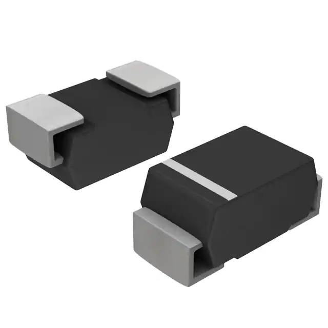
CATHODE
ANODE
SMA
CASE 403D
MARKING DIAGRAM
Mechanical Characteristics
CASE: Void-free, transfer-molded plastic
FINISH: All external surfaces are corrosion resistant and leads are
XXX
AYWWG
readily solderable
MAXIMUM CASE TEMPERATURE FOR SOLDERING PURPOSES:
260°C for 10 Seconds
POLARITY: Cathode indicated by molded polarity notch or polarity
band
XXX
A
Y
WW
G
MOUNTING POSITION: Any
= Specific Device Code
= (See Table on Page 2)
= Assembly Location
= Year
= Work Week
= Pb−Free Package
ORDERING INFORMATION
Device
Package
Shipping†
BZG03C15G
SMA
(Pb−Free)
5000/Tape & Reel
BZG03C150G
SMA
(Pb−Free)
5000/Tape & Reel
†For information on tape and reel specifications,
including part orientation and tape sizes, please
refer to our Tape and Reel Packaging Specification
Brochure, BRD8011/D.
© Semiconductor Components Industries, LLC, 2005
September, 2019 − Rev. 5
1
Publication Order Number:
BZG03C15/D
�BZG03C15 Series
MAXIMUM RATINGS
Rating
Symbol
Value
Unit
PZSM
600
W
Peak Power Dissipation (Note 1) @ TL = 25°C, tP = 100 ms
DC Power Dissipation @ TL = 75°C
Measured Zero Lead Length (Note 2)
Derate Above 75°C
Thermal Resistance, Junction−to−Lead
PD
1.5
W
RqJL
20
50
mW/°C
°C/W
Forward Surge Current (Note 3) @ TA = 25°C
IFSM
40
A
TJ, Tstg
−65 to +150
°C
Operating and Storage Temperature Range
Stresses exceeding those listed in the Maximum Ratings table may damage the device. If any of these limits are exceeded, device functionality
should not be assumed, damage may occur and reliability may be affected.
1. 100 ms, non−repetitive square pulse
2. 1 in. square copper pad, FR−4 board
3. 1/2 sine wave (or equivalent square wave), PW = 8.3 ms, duty cycle = 4 pulses per minute maximum
SYMBOLS DEFINITIONS
I
Symbol
IF
VC VBR VRWM
IPP
Maximum Reverse Peak Pulse Current
VC
Clamping Voltage @ IPP
VRWM
IR
V
IR VF
IT
Working Peak Reverse Voltage
Maximum Reverse Leakage Current @ VRWM
VBR
IPP
Parameter
Breakdown Voltage @ IT
IT
Test Current
IF
Forward Current
VF
Forward Voltage @ IF
Uni−Directional Diode
ELECTRICAL CHARACTERISTICS (TA = 25°C unless otherwise noted, VF = 1.2 V Max. @ IF = 0.5 A for all types)
Breakdown Voltage
VRWM
(Note 4)
IR @ VRWM
Volts
mA
Min
Nom
VBR (V) (Note 5)
Zzt @ IT
@ IT
Typ
Max
Max
mA
W
W
Device*
Device
Marking
BZG03C15, G
G15
11
1
13.8
15.0
15.6
50
5.0
10.0
BZG03C150, G
G150
110
1
138
150
156
5
130
300
4. A transient suppressor is normally selected according to the working peak reverse voltage (VRWM), which should be equal to or greater than
the DC or continuous peak operating voltage level
5. VBR measured at pulse test current IT at an ambient temperature of 25°C
*The “G’’ suffix indicates Pb−Free package available.
www.onsemi.com
2
�BZG03C15 Series
RATING AND TYPICAL CHARACTERISTIC CURVES
10,000
NONREPETITIVE
PULSE WAVEFORM
SHOWN IN FIGURE 2.
TA = 25°C
10
C, CAPACITANCE (pF)
Ppk , PEAK POWER (kW)
100
1
0.1
10-4
0.001
0.01
0.1
tP, PULSE WIDTH (ms)
1
MEASURED AT
ZERO BIAS
1,000
MEASURED AT
STAND-OFF
VOLTAGE, VWM
100
10
10
1
Figure 1. Pulse Rating Curve
PD , MAXIMUM POWER DISSIPATION (WATTS)
PEAK PULSE DERATING IN % OF
PEAK POWER OR CURRENT
10 x 1000 WAVEFORM
AS DEFINED BY R.E.A.
80
60
40
20
0
0
40
2
5
10
20
50
V(BR), BREAKDOWN VOLTAGE (VOLTS)
100 200
Figure 3. Typical Junction Capacitance
120
100
TJ = 25°C
f = 1 MHz
Vsig = 50 mVp-p
5
4
@ TL = 75°C
PD = 1.5 W
3
2
@ TA = 25°C
PD = 0.5 W
1
0
0
200
80
120
160
TA, AMBIENT TEMPERATURE (°C)
6
25
75
50
100
T, TEMPERATURE (°C)
125
Figure 4. Steady State Power Derating
Figure 2. Pulse Derating Curve
SURMETIC is a trademark of Semiconductor Components Industries, LLC.
www.onsemi.com
3
150
�MECHANICAL CASE OUTLINE
PACKAGE DIMENSIONS
STYLE 1
SMA
CASE 403D
ISSUE J
STYLE 2
SCALE 1:1
STYLE 1:
PIN 1. CATHODE (POLARITY BAND)
2. ANODE
DATE 22 OCT 2021
STYLE 2:
NO POLARITY
GENERIC
MARKING DIAGRAM*
xxxx
AYWWG
STYLE 1
xxxx
A
Y
WW
G
xxxx
AYWWG
STYLE 2
= Specific Device Code
= Assembly Location
= Year
= Work Week
= Pb−Free Package
*This information is generic. Please refer to
device data sheet for actual part marking.
Pb−Free indicator, “G” or microdot “G”, may
or may not be present. Some products may
not follow the Generic Marking.
DOCUMENT NUMBER:
DESCRIPTION:
98AON04079D
SMA
Electronic versions are uncontrolled except when accessed directly from the Document Repository.
Printed versions are uncontrolled except when stamped “CONTROLLED COPY” in red.
PAGE 1 OF 1
onsemi and
are trademarks of Semiconductor Components Industries, LLC dba onsemi or its subsidiaries in the United States and/or other countries. onsemi reserves
the right to make changes without further notice to any products herein. onsemi makes no warranty, representation or guarantee regarding the suitability of its products for any particular
purpose, nor does onsemi assume any liability arising out of the application or use of any product or circuit, and specifically disclaims any and all liability, including without limitation
special, consequential or incidental damages. onsemi does not convey any license under its patent rights nor the rights of others.
© Semiconductor Components Industries, LLC, 2019
www.onsemi.com
�onsemi,
, and other names, marks, and brands are registered and/or common law trademarks of Semiconductor Components Industries, LLC dba “onsemi” or its affiliates
and/or subsidiaries in the United States and/or other countries. onsemi owns the rights to a number of patents, trademarks, copyrights, trade secrets, and other intellectual property.
A listing of onsemi’s product/patent coverage may be accessed at www.onsemi.com/site/pdf/Patent−Marking.pdf. onsemi reserves the right to make changes at any time to any
products or information herein, without notice. The information herein is provided “as−is” and onsemi makes no warranty, representation or guarantee regarding the accuracy of the
information, product features, availability, functionality, or suitability of its products for any particular purpose, nor does onsemi assume any liability arising out of the application or use
of any product or circuit, and specifically disclaims any and all liability, including without limitation special, consequential or incidental damages. Buyer is responsible for its products
and applications using onsemi products, including compliance with all laws, regulations and safety requirements or standards, regardless of any support or applications information
provided by onsemi. “Typical” parameters which may be provided in onsemi data sheets and/or specifications can and do vary in different applications and actual performance may
vary over time. All operating parameters, including “Typicals” must be validated for each customer application by customer’s technical experts. onsemi does not convey any license
under any of its intellectual property rights nor the rights of others. onsemi products are not designed, intended, or authorized for use as a critical component in life support systems
or any FDA Class 3 medical devices or medical devices with a same or similar classification in a foreign jurisdiction or any devices intended for implantation in the human body. Should
Buyer purchase or use onsemi products for any such unintended or unauthorized application, Buyer shall indemnify and hold onsemi and its officers, employees, subsidiaries, affiliates,
and distributors harmless against all claims, costs, damages, and expenses, and reasonable attorney fees arising out of, directly or indirectly, any claim of personal injury or death
associated with such unintended or unauthorized use, even if such claim alleges that onsemi was negligent regarding the design or manufacture of the part. onsemi is an Equal
Opportunity/Affirmative Action Employer. This literature is subject to all applicable copyright laws and is not for resale in any manner.
PUBLICATION ORDERING INFORMATION
LITERATURE FULFILLMENT:
Email Requests to: orderlit@onsemi.com
onsemi Website: www.onsemi.com
◊
TECHNICAL SUPPORT
North American Technical Support:
Voice Mail: 1 800−282−9855 Toll Free USA/Canada
Phone: 011 421 33 790 2910
Europe, Middle East and Africa Technical Support:
Phone: 00421 33 790 2910
For additional information, please contact your local Sales Representative
�