BZX85C3V3RL Series
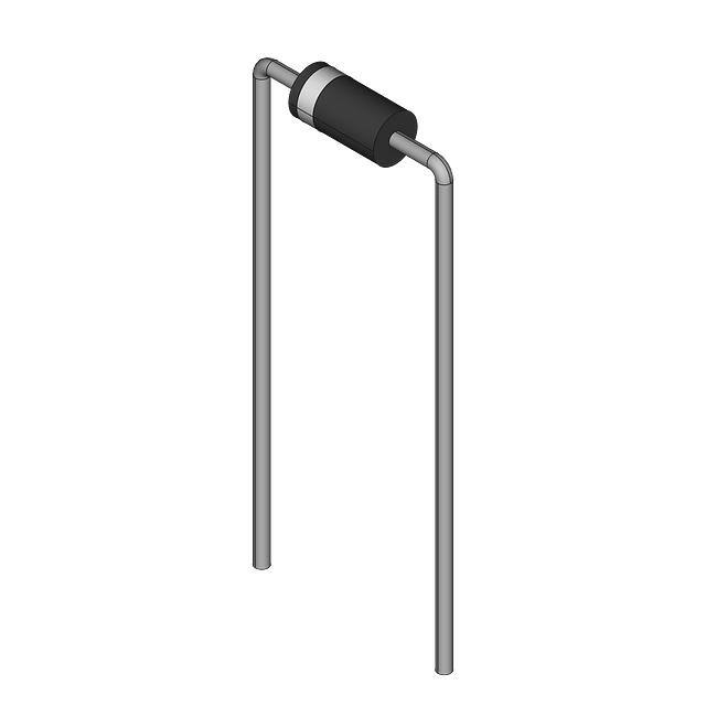
1 Watt DO-41 Hermetically
Sealed Glass Zener Voltage
Regulators
This is a complete series of 1 Watt Zener diodes with limits and
excellent operating characteristics that reflect the superior capabilities
of silicon–oxide passivated junctions. All this in an axial–lead
hermetically sealed glass package that offers protection in all common
environmental conditions.
http://onsemi.com
Cathode
Anode
Specification Features:
•
•
•
•
•
•
Zener Voltage Range – 3.3 V to 85 V
ESD Rating of Class 3 (>16 KV) per Human Body Model
DO–41 (DO–204AL) Package
Double Slug Type Construction
Metallurgical Bonded Construction
Oxide Passivated Die
AXIAL LEAD
CASE 59
GLASS
Mechanical Characteristics:
CASE: Double slug type, hermetically sealed glass
FINISH: All external surfaces are corrosion resistant and leads are
MARKING DIAGRAM
readily solderable
L
BZX
85C
xxx
YWW
MAXIMUM LEAD TEMPERATURE FOR SOLDERING PURPOSES:
230°C, 1/16″ from the case for 10 seconds
POLARITY: Cathode indicated by polarity band
MOUNTING POSITION: Any
MAXIMUM RATINGS
Rating
Max. Steady State Power Dissipation
@ TL ≤ 50°C, Lead Length = 3/8″
Derate above 50°C
Operating and Storage
Temperature Range
Symbol
Value
Unit
PD
1
W
6.67
mW/°C
–65 to
+200
°C
TJ, Tstg
L
= Assembly Location
BZX85Cxxx = Device Code
= (See Table Next Page)
Y
= Year
WW
= Work Week
ORDERING INFORMATION
Device
Package
Shipping
BZX85CxxxRL
Axial Lead
6000/Tape & Reel
BZX85CxxxRL2
Axial Lead
6000/Tape & Reel
* The “2” suffix refers to 26 mm tape spacing.
Semiconductor Components Industries, LLC, 2001
May, 2001 – Rev. 0
221
Publication Order Number:
BZX85C3V3RL/D
�BZX85C3V3RL Series
ELECTRICAL CHARACTERISTICS (TA = 25°C unless
I
otherwise noted, VF = 1.2 V Max., IF = 200 mA for all types)
Symbol
IF
Parameter
VZ
Reverse Zener Voltage @ IZT
IZT
Reverse Current
ZZT
Maximum Zener Impedance @ IZT
IZK
Reverse Current
ZZK
Maximum Zener Impedance @ IZK
IR
Reverse Leakage Current @ VR
VR
Breakdown Voltage
IF
Forward Current
VF
Forward Voltage @ IF
IR
Surge Current @ TA = 25°C
VZ VR
V
IR VF
IZT
Zener Voltage Regulator
http://onsemi.com
222
�BZX85C3V3RL Series
ELECTRICAL CHARACTERISTICS (TA = 25°C unless otherwise noted, VF = 1.2 V Max., IF = 200 mA for all types)
Zener Voltage (Notes 2. and 3.)
VZ (Volts)
Zener Impedance (Note 4.)
@ IZT
ZZT @ IZT
Leakage Current
ZZK @ IZK
IR @ VR
IR
(Note 5.)
Device
(Note 1.)
Device
Marking
Min
Nom
Max
mA
�
�
mA
µA Max
Volts
mA
BZX85C3V3RL
BZX85C3V6RL
BZX85C3V9RL
BZX85C4V3RL
BZX85C4V7RL
BZX85C3V3
BZX85C3V6
BZX85C3V9
BZX85C4V3
BZX85C4V7
3.1
3.4
3.7
4.0
4.4
3.3
3.6
3.9
4.3
4.7
3.5
3.8
4.1
4.6
5.0
80
60
60
50
45
20
15
15
13
13
400
500
500
500
600
1
1
1
1
1
1
1
1
1
1.5
60
30
5
3
3
1380
1260
1190
1070
970
BZX85C5V1RL
BZX85C5V6RL
BZX85C6V2RL
BZX85C6V8RL
BZX85C7V5RL
BZX85C5V1
BZX85C5V6
BZX85C6V2
BZX85C6V8
BZX85C7V5
4.8
5.2
5.8
6.4
7.0
5.1
5.6
6.2
6.8
7.45
5.4
6.0
6.6
7.2
7.9
45
45
35
35
35
10
7
4
3.5
3
500
400
300
300
200
1
1
1
1
0.5
2
2
3
4
4.5
1
1
1
1
1
890
810
730
660
605
BZX85C8V2RL
BZX85C9V1RL
BZX85C10RL
BZX85C12RL
BZX85C13RL
BZX85C8V2
BZX85C9V1
BZX85C10
BZX85C12
BZX85C13
7.7
8.5
9.4
11.4
12.4
8.2
9.05
10
12.05
13.25
8.7
9.6
10.6
12.7
14.1
25
25
25
20
20
5
5
7
9
10
200
200
200
350
400
0.5
0.5
0.5
0.5
0.5
5
6.5
7
8.4
9.1
1
1
0.5
0.5
0.5
550
500
454
380
344
BZX85C15RL
BZX85C16RL
BZX85C18RL
BZX85C22RL
BZX85C24RL
BZX85C15
BZX85C16
BZX85C18
BZX85C22
BZX85C24
13.8
15.3
16.8
20.8
22.8
14.7
16.2
17.95
22.05
24.2
15.6
17.1
19.1
23.3
25.6
15
15
15
10
10
15
15
20
25
25
500
500
500
600
600
0.5
0.5
0.5
0.5
0.5
10.5
11
12.5
15.5
17
0.5
0.5
0.5
0.5
0.5
304
285
250
205
190
BZX85C27RL
BZX85C30RL
BZX85C33RL
BZX85C36RL
BZX85C43RL
BZX85C27
BZX85C30
BZX85C33
BZX85C36
BZX85C43
25.1
28
31
34
40
27
30
33
36
43
28.9
32
35
38
46
8
8
8
8
6
30
30
35
40
50
750
1000
1000
1000
1000
0.25
0.25
0.25
0.25
0.25
19
21
23
25
30
0.5
0.5
0.5
0.5
0.5
170
150
135
125
110
BZX85C47RL
BZX85C62RL
BZX85C75RL
BZX85C82RL
BZX85C47
BZX85C62
BZX85C75
BZX85C82
44
58
70
77
47
62
75
82
50
66
80
87
4
4
4
2.7
90
125
150
200
1500
2000
2000
3000
0.25
0.25
0.25
0.25
33
43
51
56
0.5
0.5
0.5
0.5
95
70
60
55
1. TOLERANCE AND TYPE NUMBER DESIGNATION
The type numbers listed have zener voltage min/max limits as shown and have a standard tolerance on the nominal zener voltage of ±5%.
2. AVAILABILITY OF SPECIAL DIODES
For detailed information on price, availability and delivery of nominal zener voltages between the voltages shown and tighter voltage
tolerances, contact your nearest ON Semiconductor representative.
3. ZENER VOLTAGE (VZ) MEASUREMENT
VZ measured after the test current has been applied to 40 ±10 msec, while maintaining the lead temperature (TL) at 30°C ±1°C, 3/8″ from
the diode body.
4. ZENER IMPEDANCE (ZZ) DERIVATION
The zener impedance is derived from 1 kHz cycle AC voltage, which results when an AC current having an rms value equal to 10% of the
DC zener current (IZT or IZK) is superimposed on IZT or IZK.
5. SURGE CURRENT (IR) NON–REPETITIVE
The rating listed in the electrical characteristics table is maximum peak, non–repetitive, reverse surge current of 1/2 square wave or eqivalent
sine wave pulse of 1/120 second duration superimposed on the test current, IZT. However, actual device capability is as described in Figure
5 of the General Data – DO–41 Glass.
http://onsemi.com
223
�PD, STEADY STATE POWER DISSIPATION (WATTS)
BZX85C3V3RL Series
1.25
L = 1″
L = 1/8″
1
L = LEAD LENGTH
TO HEAT SINK
L = 3/8″
0.75
0.5
0.25
0
20
40
60
80 100 120 140
TL, LEAD TEMPERATURE (°C)
160
180
Figure 1. Power Temperature Derating Curve
http://onsemi.com
224
200
�BZX85C3V3RL Series
b. Range for Units to 12 to 100 Volts
+12
θVZ , TEMPERATURE COEFFICIENT (mV/°C)
θVZ , TEMPERATURE COEFFICIENT (mV/°C)
a. Range for Units to 12 Volts
+10
+8
+6
+4
+2
VZ�@�IZT
RANGE
0
-2
-4
2
3
4
5
6
7
8
9
VZ, ZENER VOLTAGE (VOLTS)
10
11
100
70
50
12
30
20
RANGE
10
7
5
VZ�@�IZT
3
2
1
10
20
30
50
VZ, ZENER VOLTAGE (VOLTS)
70
100
Ppk , PEAK SURGE POWER (WATTS)
175
θVZ , TEMPERATURE COEFFICIENT (mV/°C)
θ JL , JUNCTION�TO�LEAD THERMAL RESISTANCE (mV/°C/W)
Figure 2. Temperature Coefficients
(–55°C to +150°C temperature range; 90% of the units are in the ranges indicated.)
150
125
100
75
50
25
0
0
0.1
0.2
0.3
0.4
0.5
0.6
0.7
0.9
1
VZ�@�IZ
TA�=�25°C
+4
+2
20�mA
0
0.01�mA
1�mA
NOTE: BELOW 3 VOLTS AND ABOVE 8 VOLTS
NOTE: CHANGES IN ZENER CURRENT DO NOT
NOTE: EFFECT TEMPERATURE COEFFICIENTS
-2
-4
3
4
5
6
7
8
L, LEAD LENGTH TO HEAT SINK (INCHES)
VZ, ZENER VOLTAGE (VOLTS)
Figure 3. Typical Thermal Resistance
versus Lead Length
Figure 4. Effect of Zener Current
100
70
50
30
0.8
+6
RECTANGULAR
WAVEFORM
TJ�=�25°C PRIOR TO
INITIAL PULSE
11�V-100�V NONREPETITIVE
5% DUTY CYCLE
3.3�V-10�V NONREPETITIVE
20
10
7
5
3
2
1
0.01
10% DUTY CYCLE
20% DUTY CYCLE
0.02
0.05
0.1
0.2
0.5
This graph represents 90 percentile data points.
For worst case design characteristics, multiply surge power by 2/3.
1
2
5
PW, PULSE WIDTH (ms)
10
Figure 5. Maximum Surge Power
http://onsemi.com
225
20
50
100
200
500
1000
�BZX85C3V3RL Series
VZ = 2.7 V
200
1000
700
500
TJ = 25°C
iZ(rms) = 0.1 IZ(dc)
f = 60 Hz
Z Z , DYNAMIC IMPEDANCE (OHMS)
Z Z , DYNAMIC IMPEDANCE (OHMS)
1000
500
47 V
100
27 V
50
20
10
6.2 V
5
2
1
0.1
0.2
0.5
1
2
5
10
IZ, ZENER CURRENT (mA)
20
50
IZ = 1 mA
200
100
70
50
5 mA
20
20 mA
10
7
5
2
1
100
1
2
Figure 6. Effect of Zener Current
on Zener Impedance
10000
7000
5000
5
7 10
20 30
VZ, ZENER VOLTAGE (V)
50
70 100
Figure 7. Effect of Zener Voltage
on Zener Impedance
200
C, CAPACITANCE (pF)
TYPICAL LEAKAGE CURRENT
AT 80% OF NOMINAL
BREAKDOWN VOLTAGE
1000
700
500
200
100
70
50
0 V BIAS
100
1 V BIAS
50
20
10
8
20
4
10
7
5
50% OF BREAKDOWN BIAS
1
2
5
10
20
VZ, NOMINAL VZ (VOLTS)
50
100
Figure 9. Typical Capacitance versus VZ
2
1
0.7
0.5
1000
500
+125°C
0.2
I F , FORWARD CURRENT (mA)
I R , LEAKAGE CURRENT (µ A)
3
400
300
2000
0.1
0.07
0.05
0.02
0.01
0.007
0.005
+25°C
MINIMUM
MAXIMUM
200
100
50
20
75°C
10
25°C
5 150°C
0°C
2
0.002
0.001
TJ = 25°C
iZ(rms) = 0.1 IZ(dc)
f = 60 Hz
3
4
5
6
7
8
9
10
11
12
13
14
15
1
0.4
0.5
0.6
0.7
0.8
0.9
1
VZ, NOMINAL ZENER VOLTAGE (VOLTS)
VF, FORWARD VOLTAGE (VOLTS)
Figure 8. Typical Leakage Current
Figure 10. Typical Forward Characteristics
http://onsemi.com
226
1.1
�BZX85C3V3RL Series
APPLICATION NOTE
∆TJL is the increase in junction temperature above the lead
temperature and may be found as follows:
Since the actual voltage available from a given zener
diode is temperature dependent, it is necessary to determine
junction temperature under any set of operating conditions
in order to calculate its value. The following procedure is
recommended:
Lead Temperature, TL, should be determined from:
∆TJL = θJLPD.
θJL may be determined from Figure 3 for dc power
conditions. For worst-case design, using expected limits of
IZ, limits of PD and the extremes of TJ(∆TJ) may be
estimated. Changes in voltage, VZ, can then be found from:
TL = θLAPD + TA.
θLA is the lead-to-ambient thermal resistance (°C/W) and PD
is the power dissipation. The value for θLA will vary and
depends on the device mounting method. θLA is generally 30
to 40°C/W for the various clips and tie points in common use
and for printed circuit board wiring.
The temperature of the lead can also be measured using a
thermocouple placed on the lead as close as possible to the
tie point. The thermal mass connected to the tie point is
normally large enough so that it will not significantly
respond to heat surges generated in the diode as a result of
pulsed operation once steady-state conditions are achieved.
Using the measured value of TL, the junction temperature
may be determined by:
∆V = θVZ ∆TJ.
θVZ, the zener voltage temperature coefficient, is found
from Figure 2.
Under high power-pulse operation, the zener voltage will
vary with time and may also be affected significantly by the
zener resistance. For best regulation, keep current
excursions as low as possible.
Surge limitations are given in Figure 5. They are lower
than would be expected by considering only junction
temperature, as current crowding effects cause temperatures
to be extremely high in small spots, resulting in device
degradation should the limits of Figure 5 be exceeded.
TJ = TL + ∆TJL.
http://onsemi.com
227
�