H
CAT28F020
EE
GEN FR
ALO
2 Megabit CMOS Flash Memory
LE
Licensed Intel second source
FEATURES
■ Commercial, industrial and automotive
■ Fast read access time: 90/120 ns
temperature ranges
■ Low power CMOS dissipation:
■ Stop timer for program/erase
– Active: 30 mA max (CMOS/TTL levels)
– Standby: 1 mA max (TTL levels)
– Standby: 100 µA max (CMOS levels)
■ On-chip address and data latches
■ JEDEC standard pinouts:
– 32-pin DIP
– 32-pin PLCC
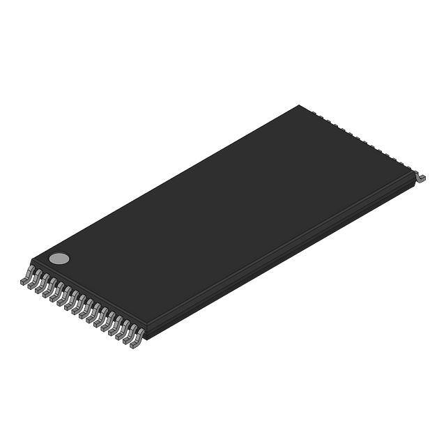
– 32-pin TSOP (8 x 20)
■ High speed programming:
– 10 µs per byte
– 4 seconds typical chip program
■ 100,000 program/erase cycles
■ 0.5 seconds typical chip-erase
■ 12.0V
A D F R E ETM
■ 10 year data retention
± 5% programming and erase voltage
■ Electronic signature
DESCRIPTION
using a two write cycle scheme. Address and Data are
latched to free the I/O bus and address bus during the
write operation.
The CAT28F020 is a high speed 256K x 8-bit electrically
erasable and reprogrammable Flash memory ideally
suited for applications requiring in-system or after-sale
code updates. Electrical erasure of the full memory
contents is achieved typically within 0.5 second.
The CAT28F020 is manufactured using Catalyst’s
advanced CMOS floating gate technology. It is designed
to endure 100,000 program/erase cycles and has a data
retention of 10 years. The device is available in JEDEC
approved 32-pin plastic DIP, 32-pin PLCC or 32-pin
TSOP packages.
It is pin and Read timing compatible with standard
EPROM and E2PROM devices. Programming and
Erase are performed through an operation and verify
algorithm. The instructions are input via the I/O bus,
BLOCK DIAGRAM
I/O0–I/O7
I/O BUFFERS
ERASE VOLTAGE
SWITCH
WE
COMMAND
REGISTER
PROGRAM VOLTAGE
SWITCH
CE, OE LOGIC
DATA
LATCH
SENSE
AMP
CE
ADDRESS LATCH
OE
A0–A17
Y-GATING
Y-DECODER
X-DECODER
VOLTAGE VERIFY
SWITCH
© 2004 by Catalyst Semiconductor, Inc.
Characteristics subject to change without notice
2,097,152 BIT
MEMORY
ARRAY
5115 FHD F02
1
Doc. No. 1029, Rev. C
�CAT28F020
PIN CONFIGURATION
PLCC Package (N, G)
32
31
30
29
28
27
26
25
24
23
22
21
20
19
18
17
VCC
WE
A17
A14
A13
A8
A9
A11
OE
A10
CE
I/O7
I/O6
I/O5
I/O4
I/O3
4 3 2 1 32 31 30
A7
A6
A5
A4
A3
A2
A1
A0
I/O0
5
6
7
8
29
28
27
26
A14
A13
A8
A9
A11
OE
A10
CE
9
25
10
24
11
23
12
22
13
21
14 15 16 17 18 19 20
I/O7
Pin Name
Type
Function
A0–A17
Input
Address Inputs for
memory addressing
I/O0–I/O7
I/O
Data Input/Output
CE
Input
Chip Enable
OE
Input
Output Enable
WE
Input
Write Enable
VCC
Voltage Supply
VSS
Ground
VPP
Program/Erase
Voltage Supply
I/O1
I/O2
VSS
I/O3
I/O4
I/O5
I/O6
1
2
3
4
5
6
7
8
9
10
11
12
13
14
15
16
A12
A15
A16
VPP
VCC
WE
A17
DIP Package (P, L)
VPP
A16
A15
A12
A7
A6
A5
A4
A3
A2
A1
A0
I/O0
I/O1
I/O2
VSS
PIN FUNCTIONS
5115 FHD F01
TSOP Package (Standard Pinout) (T, H)
A11
A9
A8
A13
A14
A17
WE
VCC
VPP
A16
A15
A12
A7
A6
A5
A4
1
2
3
4
5
6
7
8
9
10
11
12
13
14
15
16
32
31
30
29
28
27
26
25
24
23
22
21
20
19
18
17
OE
A10
CE
I/O7
I/O6
I/O5
I/O4
I/O3
VSS
I/O2
I/O1
I/O0
A0
A1
A2
A3
32
31
30
29
28
27
26
25
24
23
22
21
20
19
18
17
A11
A9
A8
A13
A14
A17
WE
VCC
VPP
A16
A15
A12
A7
A6
A5
A4
TSOP Package (Reverse Pinout) (TR, HR)
OE
A10
CE
I/O7
I/O6
I/O5
I/O4
I/O3
VSS
I/O2
I/O1
I/O0
A0
A1
A2
A3
1
2
3
4
5
6
7
8
9
10
11
12
13
14
15
16
5115 FHD F14
Doc. No. 1029, Rev. C
2
�CAT28F020
ABSOLUTE MAXIMUM RATINGS*
*COMMENT
Temperature Under Bias ................... –55°C to +95°C
Stresses above those listed under “Absolute Maximum
Ratings” may cause permanent damage to the device.
These are stress ratings only, and functional operation of
the device at these or any other conditions outside of those
listed in the operational sections of this specification is not
implied. Exposure to any absolute maximum rating for
extended periods may affect device performance and
reliability.
Storage Temperature ....................... –65°C to +150°C
Voltage on Any Pin with
Respect to Ground(1) ........... –2.0V to +VCC + 2.0V
Voltage on Pin A9 with
Respect to Ground(1) ................... –2.0V to +13.5V
VPP with Respect to Ground
during Program/Erase(1) .............. –2.0V to +14.0V
VCC with Respect to Ground(1) ............ –2.0V to +7.0V
Package Power Dissipation
Capability (TA = 25°C) .................................. 1.0 W
Lead Soldering Temperature (10 secs) ............ 300°C
Output Short Circuit Current(2) ........................ 100 mA
RELIABILITY CHARACTERISTICS
Symbol
Parameter
Test Method
Min
(3)
Endurance
MIL-STD-883, Test Method 1033
100K
Cycles/Byte
Data Retention
MIL-STD-883, Test Method 1008
10
Years
ESD Susceptibility
MIL-STD-883, Test Method 3015
2000
Volts
Latch-Up
JEDEC Standard 17
100
mA
Test
Conditions
Min
Input Pin Capacitance
COUT(3)
CVPP(3)
NEND
TDR(3)
(3)
VZAP
ILTH(3)(4)
Typ
Max
Units
CAPACITANCE TA = 25°C, f = 1.0 MHz
Symbol
CIN
(3)
Typ
Max
Units
VIN = 0V
6
pF
Output Pin Capacitance
VOUT = 0V
10
pF
VPP Supply Capacitance
VPP = 0V
25
pF
Note:
1. The minimum DC input voltage is –0.5V. During transitions, inputs may undershoot to –2.0V for periods of less than 20 ns. Maximum DC
voltage on output pins is VCC +0.5V, which may overshoot to VCC + 2.0V for periods of less than 20ns.
2. Output shorted for no more than one second. No more than one output shorted at a time.
3. This parameter is tested initially and after a design or process change that affects the parameter.
4. Latch-up protection is provided for stresses up to 100 mA on address and data pins from –1V to VCC +1V.
3
Doc. No. 1029, Rev. C
�CAT28F020
D.C. OPERATING CHARACTERISTICS
VCC = +5V ±10%, unless otherwise specified. (See Note 2)
Symbol
Parameter
ILI
Input Leakage Current
ILO
Output Leakage Current
ISB1
VCC Standby Current CMOS
ISB2
VCC Standby Current TTL
ICC1
VCC Active Read Current
ICC2(1)
VCC Programming Current
ICC3(1)
VCC Erase Current
ICC4(1)
VCC Prog./Erase Verify Current
IPPS
Test Conditions
Max
Unit
VIN = VCC or VSS
VCC = 5.5V, OE = VIH
±1
µA
VOUT = VCC or VSS,
VCC = 5.5V, OE = VIH
±1
µA
CE = VCC ±0.5V,
VCC = 5.5V
100
µA
CE = VIH, VCC = 5.5V
1
mA
VCC = 5.5V, CE = VIL,
IOUT = 0mA, f = 6 MHz
30
mA
VCC = 5.5V,
Programming in Progress
15
mA
VCC = 5.5V,
Erasure in Progress
15
mA
VCC = 5.5V, Program or
Erase Verify in Progress
15
mA
VPP Standby Current
VPP = VPPL
±10
µA
IPP1
VPP Read Current
VPP = VPPH
200
µA
IPP2(1)
VPP Programming Current
VPP = VPPH,
Programming in Progress
30
mA
IPP3(1)
VPP Erase Current
VPP = VPPH,
Erasure in Progress
30
mA
IPP4(1)
VPP Prog./Erase Verify Current
VPP = VPPH, Program or
Erase Verify in Progress
5
mA
VIL
Input Low Level TTL
-0.5
0.8
V
VILC
Input Low Level CMOS
-0.5
0.8
V
0.45
V
IOL = 5.8mA, VCC
Min
(2)
= 4.5V
Typ
VOL
Output Low Level
VIH
Input High Level TTL
2
VCC+0.5
V
VIHC
Input High Level CMOS
VCC*0.7
VCC+0.5
V
VOH1
Output High Level TTL
IOH = -2.5mA, VCC(2) = 4.5V
VOH2
Output High Level CMOS
IOH = -400µA,
VID
A9 Signature Voltage
A9 = VID
IID(1)
A9 Signature Current
A9 = VID
VLO
VCC Erase/Prog. Lockout Voltage
VCC(2)
2.4
= 4.5V VCC-0.4
11.4
2.5
Note:
1. This parameter is tested initially and after a design or process change that affects the parameter.
2. CAT28F020-90, VCCMIN = 4.75 V.
Doc. No. 1029, Rev. C
4
V
V
13
V
200
µA
V
�CAT28F020
SUPPLY CHARACTERISTICS
Symbol
Parameter
Min
VCC
VCC Supply Voltage
Typ
Max
Unit
28F020-90
4.75
5.5
V
28F020-12
4.5
5.5
V
VPPL
VPP During Read Operations
0
6.5
V
VPPH
VPP During Read/Erase/Program
11.4
12.6
V
A.C. CHARACTERISTICS, Read Operation
VCC = +5V ±10%, unless otherwise specified. (See Note 8)
28F020-90(7)
JEDEC Standard
Symbol
Symbol
tAVAV
Parameter
Min
tRC
Read Cycle Time
90
tELQV
tCE
CE Access Time
90
120
ns
tAVQV
tACC
Address Access Time
90
120
ns
tGLQV
tOE
OE Access Time
35
50
ns
tAXQX
tOH
Output Hold from Address OE/CE Change
0
0
ns
tGLQX
tOLZ(1)(6)
OE to Output in Low-Z
0
0
ns
tELQX
tLZ(1)(6)
CE to Output in Low-Z
0
0
ns
tGHQZ
tDF(1)(2)
OE High to Output High-Z
30
30
ns
tEHQZ
tDF(1)(2)
CE High to Output High-Z
40
40
ns
tWHGL(1)
-
Write Recovery Time Before Read
Typ
Max
28F020-12(7)
Min
Typ Max
120
6
6
Unit
ns
µs
Figure 1. A.C. Testing Input/Output Waveform(3)(4)(5)
2.4 V
2.0 V
INPUT PULSE LEVELS
REFERENCE POINTS
0.8 V
0.45 V
Testing Load Circuit (example)
1.3V
1N914
3.3K
DEVICE
UNDER
TEST
OUT
CL = 100 pF
C INCLUDES JIG CAPACITANCE
L
Note:
1. This parameter is tested initially and after a design or process change that affects the parameter.
2. Output floating (High-Z) is defined as the state where the external data line is no longer driven by the output buffer.
3. Input Rise and Fall Times (10% to 90%) < 10 ns.
4. Input Pulse Levels = 0.45 V and 2.4 V. For High Speed Input Pulse Levels 0.0 V and 3.0 V.
5. Input and Output Timing Reference = 0.8 V and 2.0 V. For High Speed Input and Output Timing Reference = 1.5 V.
6. Low-Z is defined as the state where the external data may be driven by the output buffer but may not be valid.
7. For load and reference points, see Fig. 1.
8. CAT28F020-90, VCCMIN = 4.75 V.
5
Doc. No. 1029, Rev. C
�CAT28F020
A.C. CHARACTERISTICS, Program/Erase Operation
VCC = +5V ±10%, unless otherwise specified. (See Note 6)
JEDEC
Standard
Symbol
Symbol
28F020-90
tAVAV
tWC
Write Cycle Time
90
120
ns
tAVWL
tAS
Address Setup Time
0
0
ns
tWLAX
tAH
Address Hold Time
40
40
ns
tDVWH
tDS
Data Setup Time
40
40
ns
tWHDX
tDH
Data Hold Time
10
10
ns
tELWL
tCS
CE Setup Time
0
0
ns
tWHEH
tCH
CE Hold Time
0
0
ns
tWLWH
tWP
WE Pulse Width
40
40
ns
tWHWL
Parameter
Min
Typ
28F020-12
Max
Min
Typ
Max
Unit
tWPH
WE High Pulse Width
20
20
ns
(2)
-
Program Pulse Width
10
10
µs
tWHWH2(2)
-
Erase Pulse Width
9.5
9.5
ms
tWHGL
-
Write Recovery Time Before Read
6
6
µs
tGHWL
-
Read Recovery Time Before Write
0
0
µs
tVPEL
-
VPP Setup Time to CE
100
100
ns
tWHWH1
ERASE AND PROGRAMMING PERFORMANCE(1)
28F020-90
Parameter
Chip Erase
Min
Time(3)(5)
28F020-12
Typ
Max
0.5
4
Chip Program Time(3)(4)
Min
Typ
Max
Unit
10
0.5
10
sec
25
4
25
sec
Note:
1. Please refer to Supply characteristics for the value of VPPH and VPPL. The VPP supply can be either hardwired or switched. If VPP is switched,
VPPL can be ground, less than VCC + 2.0V or a no connect with a resistor tied to ground.
2. Program and Erase operations are controlled by internal stop timers.
3. ‘Typicals’ are not guaranteed, but based on characterization data. Data taken at 25°C, 12.0V VPP.
4. Minimum byte programming time (excluding system overhead) is 16 µs (10 µs program + 6 µs write recovery), while maximum is 400 µs/
byte (16 µs x 25 loops). Max chip programming time is specified lower than the worst case allowed by the programming algorithm since
most bytes program significantly faster than the worst case byte.
5. Excludes 00H Programming prior to Erasure.
6. CAT28F020-90, VCCMIN = 4.75 V
Doc. No. 1029, Rev. C
6
�CAT28F020
FUNCTION TABLE(1)
Pins
Mode
CE
OE
WE
VPP
I/O
Notes
Read
VIL
VIL
VIH
VPPL
DOUT
Output Disable
VIL
VIH
VIH
X
High-Z
Standby
VIH
X
X
VPPL
High-Z
Signature (MFG)
VIL
VIL
VIH
X
31H
A0 = VIL, A9 = 12V
Signature (Device)
VIL
VIL
VIH
X
BDH
A0 = VIH, A9 = 12V
Program/Erase
VIL
VIH
VIL
VPPH
DIN
See Command Table
Write Cycle
VIL
VIH
VIL
VPPH
DIN
During Write Cycle
Read Cycle
VIL
VIL
VIH
VPPH
DOUT
During Write Cycle
WRITE COMMAND TABLE
Commands are written into the command register in one or two write cycles. The command register can be altered
only when VPP is high and the instruction byte is latched on the rising edge of WE. Write cycles also internally latch
addresses and data required for programming and erase operations.
Pins
First Bus Cycle
Mode
Second Bus Cycle
Operation
Address
DIN
Operation
Address
DIN
DOUT
Set Read
Write
X
00H
Read
AIN
DOUT
Read Sig. (MFG)
Write
X
90H
Read
00
31H
Read Sig. (Device)
Write
X
90H
Read
01
BDH
Erase
Write
X
20H
Write
X
Erase Verify
Write
AIN
A0H
Read
X
Program
Write
X
40H
Write
AIN
Program Verify
Write
X
C0H
Read
X
Reset
Write
X
FFH
Write
X
20H
DOUT
DIN
DOUT
FFH
Note:
1. Logic Levels: X = Logic ‘Do not care’ (VIH, VIL, VPPL, VPPH)
7
Doc. No. 1029, Rev. C
�CAT28F020
The conventional mode is entered as a regular READ
mode by driving the CE and OE pins low (with WE high),
and applying the required high voltage on address pin A9
while all other address lines are held at VIL.
READ OPERATIONS
Read Mode
A Read operation is performed with both CE and OE low
and with WE high. VPP can be either high or low,
however, if VPP is high, the Set READ command has to
be sent before reading data (see Write Operations). The
data retrieved from the I/O pins reflects the contents of
the memory location corresponding to the state of the 18
address pins. The respective timing waveforms for the
read operation are shown in Figure 3. Refer to the AC
Read characteristics for specific timing parameters.
A Read cycle from address 0000H retrieves the binary
code for the IC manufacturer on outputs I/O0 to I/O7:
CATALYST Code = 00110001 (31H)
A Read cycle from address 0001H retrieves the binary
code for the device on outputs I/O0 to I/O7.
28F020 Code = 1011 1101 (BDH)
Signature Mode
Standby Mode
The signature mode allows the user to identify the IC
manufacturer and the type of device while the device
resides in the target system. This mode can be activated
in either of two ways; through the conventional method
of applying a high voltage (12V) to address pin A9 or by
sending an instruction to the command register (see
Write Operations).
With CE at a logic-high level, the CAT28F020 is placed
in a standby mode where most of the device circuitry is
disabled, thereby substantially reducing power consumption. The outputs are placed in a high-impedance
state.
Figure 3. A.C. Timing for Read Operation
POWER UP
STANDBY
DEVICE AND
ADDRESS SELECTION
ADDRESSES
OUPUTS
ENABLED
DATA VALID
STANDBY
POWER DOWN
ADDRESS STABLE
tAVAV (tRC)
CE (E)
tEHQZ (tDF)
OE (G)
tWHGL
tGHQZ (tDF)
tGLQV (tOE)
WE (W)
tELQV (tCE)
tAXQX (tOH)
tGLQX (tOLZ)
tELQX (tLZ)
HIGH-Z
HIGH-Z
DATA (I/O)
OUTPUT VALID
tAVQV (tACC)
28F020 F05
Doc. No. 1029, Rev. C
8
�CAT28F020
A Read cycle from address 0001H retrieves the binary
code for the device on outputs I/O0 to I/O7.
WRITE OPERATIONS
The following operations are initiated by observing the
sequence specified in the Write Command Table.
28F020 Code = 1011 1101 (BDH)
Read Mode
Erase Mode
The device can be put into a standard READ mode by
initiating a write cycle with 00H on the data bus. The
subsequent read cycles will be performed similar to a
standard EPROM or E2PROM Read.
During the first Write cycle, the command 20H is written
into the command register. In order to commence the
erase operation, the identical command of 20H has to be
written again into the register. This two-step process
ensures against accidental erasure of the memory contents. The final erase cycle will be stopped at the rising
edge of WE, at which time the Erase Verify command
(A0H) is sent to the command register. During this cycle,
the address to be verified is sent to the address bus and
latched when WE goes low. An integrated stop timer
allows for automatic timing control over this operation,
eliminating the need for a maximum erase timing specification. Refer to AC Characteristics (Program/Erase)
for specific timing parameters.
Signature Mode
An alternative method for reading device signature (see
Read Operations Signature Mode), is initiated by writing
the code 90H into the command register while keeping
VPP high. A read cycle from address 0000H with CE and
OE low (and WE high) will output the device signature.
CATALYST Code = 00110001 (31H)
Figure 4. A.C. Timing for Erase Operation
VCC POWER-UP
& STANDBY
SETUP ERASE
COMMAND
ERASE
COMMAND
ERASING
ERASE VERIFY
COMMAND
ERASE
VCC POWER-DOWN/
VERIFICATION
STANDBY
ADDRESSES
tWC
tWC
tWC
tAS
tRC
tAH
CE (E)
tCH
tCS
tCH
tCS
tCH
tEHQZ
OE (G)
tGHWL
tWHWH2
tWPH
tDF
tWHGL
WE (W)
tWP
tDS
HIGH-Z
DATA IN
= 20H
DATA (I/O)
tDH
tDS
tWP
tDH
tWP
tDS
tDH
tOE
tOH
tOLZ
DATA IN
= A0H
DATA IN
= 20H
tLZ
tCE
VALID
DATA OUT
VCC 5.0V
0V
tVPEL
VPP VPPH
VPPL
28F020 F11
9
Doc. No. 1029, Rev. C
�CAT28F020
Figure 5. Chip Erase Algorithm(1)
BUS
OPERATION COMMAND
START ERASURE
COMMENTS
VPP RAMPS TO VPPH
(OR VPP HARDWIRED)
APPLY VPPH
PROGRAM ALL
BYTES TO 00H
ALL BYTES SHALL BE
PROGRAMMED TO 00
BEFORE AN ERASE
OPERATION
STANDBY
INITIALIZE
ADDRESS
INITIALIZE ADDRESS
INITIALIZE
PLSCNT = 0
PLSCNT = PULSE COUNT
WRITE ERASE
SETUP COMMAND
WRITE
ERASE
ACTUAL ERASE
NEEDS
10ms PULSE,
DATA=20H
DATA = 20H
WRITE ERASE
COMMAND
WRITE
ERASE
DATA = 20H
DATA = 20H
WAIT
TIME OUT 10ms
WRITE ERASE
VERIFY COMMAND
WRITE
ERASE
VERIFY
TIME OUT 6µs
ADDRESS = BYTE TO VERIFY
DATA = 20H;
A0H
STOPS ERASE OPERATION
WAIT
INCREMENT
ADDRESS
READ DATA
FROM DEVICE
READ
READ BYTE TO
VERIFY ERASURE
STANDBY
COMPARE OUTPUT TO FF
INCREMENT PULSE COUNT
NO
DATA =
FFH?
YES
NO
NO
INC PLSCNT
==1000
3000 ??
YES
LAST
ADDRESS?
YES
WRITE READ
COMMAND
WRITE
APPLY VPPL
APPLY VPPL
ERASURE
COMPLETED
ERASE
ERROR
STANDBY
Note:
(1) The algorithm MUST BE FOLLOWED to ensure proper and reliable operation of the device.
Doc. No. 1029, Rev. C
10
READ
DATA = 00H
RESETS THE REGISTER
FOR READ OPERATION
VPP RAMPS TO VPPL
(OR VPP HARDWIRED)
5108 FHD F10
�CAT28F020
Erase-Verify Mode
Program-Verify Mode
The Erase-verify operation is performed on every byte
after each erase pulse to verify that the bits have been
erased.
A Program-verify cycle is performed to ensure that all
bits have been correctly programmed following each
byte programming operation. The specific address is
already latched from the write cycle just completed, and
stays latched until the verify is completed. The Programverify operation is initiated by writing C0H into the
command register. An internal reference generates the
necessary high voltages so that the user does not need
to modify VCC. Refer to AC Characteristics (Program/
Erase) for specific timing parameters.
Programming Mode
The programming operation is initiated using the programming algorithm of Figure 7. During the first write
cycle, the command 40H is written into the command
register. During the second write cycle, the address of
the memory location to be programmed is latched on the
falling edge of WE, while the data is latched on the rising
edge of WE. The program operation terminates with the
next rising edge of WE. An integrated stop timer allows
for automatic timing control over this operation, eliminating the need for a maximum program timing specification. Refer to AC Characteristics (Program/Erase) for
specific timing parameters.
Figure 6. A.C. Timing for Programming Operation
PROGRAM
VCC POWER-UP SETUP PROGRAM LATCH ADDRESS
COMMAND
& DATA
VERIFY
& STANDBY
PROGRAMMING COMMAND
PROGRAM VCC POWER-DOWN/
VERIFICATION
STANDBY
ADDRESSES
tWC
tWC
tAS
tRC
tAH
CE (E)
tCH
tCS
tCH
tCS
tCH
tEHQZ
OE (G)
tGHWL
tWHWH1
tWPH
tDF
tWHGL
WE (W)
tWP
tDS
HIGH-Z
DATA IN
= 40H
DATA (I/O)
tDH
tDS
tWP
tDH
tWP
tDS
tDH
tOE
DATA IN
= C0H
DATA IN
tLZ
tCE
VCC
VALID
DATA OUT
5.0V
0V
VPP
tOH
tOLZ
tVPEL
VPPH
VPPL
28F020 F07
11
Doc. No. 1029, Rev. C
�CAT28F020
Figure 7. Programming Algorithm(1)
START
PROGRAMMING
BUS
OPERATION
APPLY VPPH
STANDBY
COMMAND
COMMENTS
VPP RAMPS TO VPPH
(OR VPP HARDWIRED)
INITIALIZE
ADDRESS
INITIALIZE ADDRESS
PLSCNT = 0
INITIALIZE PULSE COUNT
PLSCNT = PULSE COUNT
WRITE SETUP
PROG. COMMAND
1ST WRITE
CYCLE
WRITE
SETUP
DATA = 40H
WRITE PROG. CMD
ADDR AND DATA
2ND WRITE
CYCLE
PROGRAM
VALID ADDRESS AND DATA
TIME OUT 10µs
WAIT
1ST WRITE
CYCLE
WRITE PROGRAM
VERIFY COMMAND
PROGRAM
VERIFY
TIME OUT 6µs
DATA = C0H
WAIT
READ DATA
FROM DEVICE
READ
READ BYTE TO VERIFY
PROGRAMMING
STANDBY
COMPARE DATA OUTPUT
TO DATA EXPECTED
NO
VERIFY
DATA ?
YES
INCREMENT
ADDRESS
NO
NO
INC
PLSCNT
= 25 ?
YES
LAST
ADDRESS?
YES
1ST WRITE
CYCLE
WRITE READ
COMMAND
APPLY VPPL
APPLY VPPL
PROGRAMMING
COMPLETED
PROGRAM
ERROR
STANDBY
READ
DATA = 00H
SETS THE REGISTER FOR
READ OPERATION
VPP RAMPS TO VPPL
(OR VPP HARDWIRED)
Note:
(1) The algorithm MUST BE FOLLOWED to ensure proper and reliable operation of the device.
5108 FHD F06
Doc. No. 1029, Rev. C
12
�CAT28F020
Abort/Reset
POWER SUPPLY DECOUPLING
An Abort/Reset command is available to allow the user
to safely abort an erase or program sequence. Two
consecutive program cycles with FFH on the data bus
will abort an erase or a program operation. The abort/
reset operation can interrupt at any time in a program or
erase operation and the device is reset to the Read
Mode.
To reduce the effect of transient power supply voltage
spikes, it is good practice to use a 0.1µF ceramic
capacitor between VCC and VSS and VPP and VSS. These
high-frequency capacitors should be placed as close as
possible to the device for optimum decoupling.
POWER UP/DOWN PROTECTION
The CAT28F020 offers protection against inadvertent
programming during VPP and VCC power transitions.
When powering up the device there is no power-on
sequencing necessary. In other words, VPP and VCC
may power up in any order. Additionally VPP may be
hardwired to VPPH independent of the state of VCC and
any power up/down cycling. The internal command
register of the CAT28F020 is reset to the Read Mode on
power up.
Figure 8. Alternate A.C. Timing for Program Operation
PROGRAM
VCC POWER-UP SETUP PROGRAM LATCH ADDRESS
COMMAND
& DATA
VERIFY
& STANDBY
PROGRAMMING COMMAND
PROGRAM VCC POWER-DOWN/
VERIFICATION
STANDBY
ADDRESSES
tWC
tWC
tAVEL
tRC
tELAX
WE (W)
tWLEL
tEHWH
tWLEL
tEHWH
tEHWH
tEHQZ
tWLEL
OE (G)
tEHEH
tGHEL
tEHGL
tDF
tEHEL
CE (E)
tDVEH
HIGH-Z
DATA (I/O)
tEHDX
tELEH
tDVEH
DATA IN
= 40H
tOE
tEHDX
tOLZ
tELEH
tEHDX
tDVEH
tOH
DATA IN
= C0H
DATA IN
tLZ
tCE
VALID
DATA OUT
VCC 5.0V
0V
tVPEL
VPP VPPH
VPPL
28F020 F09
28F020 F09
13
Doc. No. 1029, Rev. C
�CAT28F020
ALTERNATE CE
CE-CONTROLLED WRITES
JEDEC Standard
Symbol Symbol
28F020-90
Parameter
Min
Typ
Max
28F020-12
Min
Typ
Max
Unit
tAVAV
tWC
Write Cycle Time
90
120
ns
tAVEL
tAS
Address Setup Time
0
0
ns
tELAX
tAH
Address Hold Time
40
40
ns
tDVEH
tDS
Data Setup Time
40
40
ns
tEHDX
tDH
Data Hold Time
10
10
ns
tEHGL
—
Write Recovery Time Before Read
6
6
µs
tGHEL
—
Read Recovery Time Before Write
0
0
µs
tWLEL
tWS
WE Setup Time Before CE
0
0
ns
tEHWH
—
WE Hold Time After CE
0
0
ns
tELEH
tCP
Write Pulse Width
40
40
ns
tEHEL
tCPH
Write Pulse Width High
20
20
ns
tVPEL
—
VPP Setup Time to CE Low
100
100
ns
I
-12
ORDERING INFORMATION
Prefix
Device #
CAT
28F020
Product
Number
Optional
Company ID
Suffix
N
Temperature Range
Blank = Commercial (0ßC to +70ßC)
I = Industrial (-40ßC to +85ßC)
A = Automotive (-40ßC to +105ßC)
*
Package
N: PLCC
P: PDIP
T: TSOP (8mmx20mm)
TR: TSOP (Reverse Pinout)
G: PLCC (Lead free, Halogen free)
L: PDIP (Lead free, Halogen free)
H: TSOP (Lead free, Halogen free)
HR: TSOP (Reverse Pinout) (Lead free, Halogen free)
T
Tape & Reel
T: 500/Reel
Speed
90: 90ns
12: 120ns
* -40˚ to +125˚ is available upon request.
Note:
(1) The device used in the above example is a CAT28F020NI-12T (PLCC, Industrial Temperature, 120 ns access time, Tape & Reel).
Doc. No. 1029, Rev. C
14
�REVISION HISTORY
Date
Rev.
Reason
5/1/2002
A
Initial issue
2/10/2004
B
Change VCCMIN for CAT28F020-90 to 4.75 V from 4.5 V
7/1/2004
C
Added Green Packages in all areas.
Copyrights, Trademarks and Patents
Trademarks and registered trademarks of Catalyst Semiconductor include each of the following:
DPP ™
AE2 ™
Catalyst Semiconductor has been issued U.S. and foreign patents and has patent applications pending that protect its products. For a complete list of patents
issued to Catalyst Semiconductor contact the Company’s corporate office at 408.542.1000.
CATALYST SEMICONDUCTOR MAKES NO WARRANTY, REPRESENTATION OR GUARANTEE, EXPRESS OR IMPLIED, REGARDING THE SUITABILITY OF ITS
PRODUCTS FOR ANY PARTICULAR PURPOSE, NOR THAT THE USE OF ITS PRODUCTS WILL NOT INFRINGE ITS INTELLECTUAL PROPERTY RIGHTS OR THE
RIGHTS OF THIRD PARTIES WITH RESPECT TO ANY PARTICULAR USE OR APPLICATION AND SPECIFICALLY DISCLAIMS ANY AND ALL LIABILITY ARISING
OUT OF ANY SUCH USE OR APPLICATION, INCLUDING BUT NOT LIMITED TO, CONSEQUENTIAL OR INCIDENTAL DAMAGES.
Catalyst Semiconductor products are not designed, intended, or authorized for use as components in systems intended for surgical implant into the body, or
other applications intended to support or sustain life, or for any other application in which the failure of the Catalyst Semiconductor product could create a
situation where personal injury or death may occur.
Catalyst Semiconductor reserves the right to make changes to or discontinue any product or service described herein without notice. Products with data sheets
labeled "Advance Information" or "Preliminary" and other products described herein may not be in production or offered for sale.
Catalyst Semiconductor advises customers to obtain the current version of the relevant product information before placing orders. Circuit diagrams illustrate
typical semiconductor applications and may not be complete.
Catalyst Semiconductor, Inc.
Corporate Headquarters
1250 Borregas Avenue
Sunnyvale, CA 94089
Phone: 408.542.1000
Fax: 408.542.1200
www.catalyst-semiconductor.com
Publication #:
Revison:
Issue date:
1029
C
7/1/04
�