CAT3211
I2C Programmable Haptic
Driver for Rotary (ERM) DC
Motors
Description
The CAT3211 is an H−Bridge motor driver IC that includes an I2C
programmable haptic generator state machine, internal oscillator and
adjustable LDO voltage regulator, all in one compact solution.
Two operating modes are supported: haptic mode (triggered via
H_TRIG pin or register) and vibrator mode (VIB_EN pin or register).
H−TRIG triggers a haptic sequence where Forward, Coast, Reverse
and Recovery time durations are controlled. All four timer durations
are configured via I2C interface registers.
The LDO output voltage supplying the H−Bridge can be
programmed from 2.0 V to 5.0 V or shorted to VIN (using LDOH
register). This allows the motor to be safely overdriven for short
durations, greatly increasing the user experience.
Driving VIB_EN high sets the H−Bridge to forward direction and
LDO voltage to a predefined vibrator setting (using LDOV register).
The motor can be continuously and safely driven at low voltages in
vibrator mode.
The device is fully protected against POS, NEG and REG short and
over current conditions. Thermal shutdown protection prevents
damage to the device and system during over temperature junction
conditions.
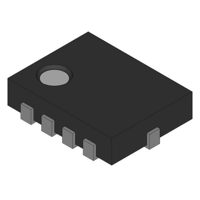
UQFN12 1.7 x 2 mm package is ideal for space constrained
applications.
Features
•
•
•
•
•
•
•
•
•
•
•
•
Haptic Generator Mode with Programmable Timers
Internal 1 ms Oscillator ±20%
600 mA Output Drive Current
High Speed 400 kHz I2C Interface
Internal LDO with Mode Adjustable Output Voltage
Supply Voltage Range from 2.7 V to 5.5 V
Internal H−Bridge Driver (0.8 W typ.)
1 Amp Diode Clamping Capability (H−Bridge & LDO)
Zero Current Shutdown Mode
Thermal Shutdown and Over−current Protection
Small 1.7 mm x 2 mm, 12−lead UQFN Package
These Devices are Pb−Free and are RoHS Compliant
http://onsemi.com
1
UQFN12
MU SUFFIX
CASE 523AE
MARKING DIAGRAM
KAM
G
KA = Specific Device Code
M = Date Code
G
= Pb−Free Package
PIN CONNECTIONS
1
GND
RST
VIB_EN
SDA
H_TRIG
SCL
OSC
VIN
REG
NEG
POS
PGND
(Top View)
ORDERING INFORMATION
Device
Package
Shipping†
CAT3211MUTAG
UQFN12
(Pb−Free)
3000/
Tape & Reel
†For information on tape and reel specifications,
including part orientation and tape sizes, please
refer to our Tape and Reel Packaging Specification
Brochure, BRD8011/D.
Typical Applications
• Eccentric Rotating Mass (ERM) Motor Control
• Haptic Vibrators in Mobile Devices
© Semiconductor Components Industries, LLC, 2013
April, 2013 − Rev. 0
1
Publication Order Number:
CAT3211/D
�CAT3211
Figure 1. Typical Application Circuit
Table 1. ABSOLUTE MAXIMUM RATINGS
Parameter
Rating
Unit
6
V
6 to (GND − 0.3)
V
(VIN + 0.3) to (GND − 0.3)
V
(REG + 1.5) to (PGND − 0.3)
V
Storage Temperature Range
−65 to +150
°C
Junction Temperature Range
+150
°C
Lead Temperature
300
°C
ESD Immunity
Human Body Model per Standard JESD22−A114E
Machine Model per Standard JESD22−A115−A
2000
200
Latch−up Immunity per Standard JESD78
Logic Pins
POS and NEG Pins
100
600
VIN
H_TRIG, VIB_EN, SDA, SCL, OSC, RST Voltage
REG Voltage
POS, NEG Voltage
V
mA
Stresses exceeding Maximum Ratings may damage the device. Maximum Ratings are stress ratings only. Functional operation above the
Recommended Operating Conditions is not implied. Extended exposure to stresses above the Recommended Operating Conditions may affect
device reliability.
Table 2. RECOMMENDED OPERATING CONDITIONS
Parameter
Rating
Unit
VIN
2.7 to 5.5
V
Ambient Temperature Range
−40 to +85
°C
POS and NEG Pin Current (Motor Current)
0 to ±600
mA
Table 3. ELECTRICAL OPERATING CHARACTERISTICS (Note 1)
(Typical values: VIN = 5.0 V, RST = Logic High, TAMB = 25°C unless otherwise specificed.)
Parameter
Symbol
Test Conditions
Min
Typ
Max
Units
Operating Current in Haptic Mode (no load)
on VIN pin
IQH
Haptic Mode triggered,
CHIP_EN = 1 (register)
270
600
mA
Operating Current in Vibrator Mode (no load)
on VIN pin
IQV
VIB_EN = High, RST = High,
CHIP_EN = 1 (register)
190
600
mA
Standby Current on VIN pin
ISTBY
VIB_EN = Low
Haptic Mode NOT triggered
1
20
mA
Shutdown Current
ISHDN
RST = Low
POS and NEG Shorted
1
mA
1.6
W
H−Bridge Output Drive Resistance (Note 2)
RHBRDG
VIB_EN = High, REG = VIN,
ILOAD = 100 mA
0.8
1. Limits are fully tested at TAMB = 25°C and guaranteed across temperature by design and characterization statistical analysis.
2. Total combined resistance of high−side and low−side switched (measured at 100 mA load). Does not include LDO Switch Resistance.
3. Limits guaranteed by design and statistical analysis.
http://onsemi.com
2
�CAT3211
Table 3. ELECTRICAL OPERATING CHARACTERISTICS (Note 1)
(Typical values: VIN = 5.0 V, RST = Logic High, TAMB = 25°C unless otherwise specificed.)
Parameter
Symbol
Test Conditions
Min
Typ
REG Output Voltage Accuracy
VREG
Any Programmed Voltage
(2.0 V to 5.0 V) LDOV & LDOH
LDO Voltage Regulator Dropout Resistance
RLDO
V_LDO = 00h & VIB_EN = 1
ILOAD = 100 mA
0.4
IP_REG
VIN = 5V, REG = GND,
no load (POS, NEG floating)
Shutdown and Standby Mode
1
REG Pin Pull−up Current to VIN
−5
Output Drive Current
IOUT
Headroom:
VIN – | VPOS −VNEG | = 1.2 V
600
Output Short Circuit Current Limit (Note 3)
ISC
POS and NEG Pin Shorted
600
H_TRIG, VIB_EN,OSC, RST Pins
Internal pull−down resistor
H_TRIG, VIB_EN,OSC,SDA,SCL, RST Pins
Logic High Input Voltage
Logic Low Input Voltage
RIN
Max
Units
+5
%
0.8
W
mA
mA
850
1000
110
VIH
VIL
1.4
mA
kW
0.4
V
V
Thermal Shutdown (Note 3)
TSD
140
°C
Thermal Hysteresis (Note 3)
THYS
20
°C
Under−Voltage Lockout (UVLO)
VUVLO
2.0
V
1. Limits are fully tested at TAMB = 25°C and guaranteed across temperature by design and characterization statistical analysis.
2. Total combined resistance of high−side and low−side switched (measured at 100 mA load). Does not include LDO Switch Resistance.
3. Limits guaranteed by design and statistical analysis.
Table 4. TIMING CHARACTERISTICS (Note 4)
(Typical values: VIN = 5.0 V, RST = Logic High, TAMB = 25°C unless otherwise specificed.)
Name
Internal Clock Period (OSC)
Symbol
Conditions
Min
Typ
Max
1
Units
TOSC
Reg EXT_OSC (00hB0) = 0
Internal Clock Accuracy (OSC)
TOSC_ACC
Reg EXT_OSC (00hB0) = 0
−20
+20
%
External Clock Period (OSC Pin) (Note 5)
TOSCEXT
Reg EXT_OSC (00hB0) = 1
1
2000
ms
External Clock Timeout (OSC Pin)
TOSCWD
Reg EXT_OSC (00hB0) = 1
Rising Edge to Rising Edge
6
10
ms
8
ms
Clock OSC Low Time
TOSCL_MIN
0.3
ms
Clock OSC High Time
TOSCH_MIN
0.2
ms
H_TRIG High Duration (Note 5)
THTRIG_MIN
200
ns
VIB_EN Rising to POS/NEG Drive Delay
TVIB_R
40
ms
VIB_EN Falling to POS/NEG Float Delay
TVIB_F
0.3
ms
H_TRIG Trigger to POS/NEG Drive Delay
TTRIG_R
40
ms
2
ms
Direction Break−Before−Make Delay
TBBM
Haptic mode forward to
reverse (no coast)
4. Limits are fully tested at TAMB = 25°C and guaranteed across temperature by design and characterization statistical analysis.
5. Limits guaranteed by design and statistical analysis.
http://onsemi.com
3
�CAT3211
NOTE: Above example has LDOV (REG) = 1Ah and LDOH (REG) = 00h.
Figure 2. Haptic/Vibrator Mode Timing Diagram
Figure 3. Haptic Power−Up Response (TTRIG_R)
(100 mA resistive load)
Figure 4. Haptic Forward−Reverse Transition
(100 mA resistive load)
http://onsemi.com
4
�CAT3211
Table 5. I2C TIMING CHARACTERISTICS
(Typical values: VIN = 5.0 V, RST = Logic High, TAMB = 25°C unless otherwise specificed.) (Note 6)
Max
Unit
fSCL
Interface Clock Frequency (Note 6)
Parameter
400
kHz
tAA
SCL Low to SDA Data Out and ACK Out
0.9
ms
tBUF
Bus Free Time Before a New Transmission Can Start
1.2
ms
Start Condition Hold Time
0.6
ms
tLOW
Clock Low Period
1.2
ms
tHIGH
Clock High Period
0.6
ms
Symbol
tHD:STA
Min
Typ
tSU:STA
Start Condition Setup Time (For a Repeated Condition)
0.6
ms
tHD:DAT
Data In Hold Time
0
ns
tSU:DAT
Data In Setup Time
100
ns
tR
SDA and SCL Rise Time (Note 6)
0.3
ms
tF
SDA and SCL Fall Time (Note 6)
300
ns
tSU:STO
tDH
Stop Condition Setup Time
0.6
ms
Data Out Hold Time
50
ns
6. Limits guaranteed by design and statistical analysis.
tHIGH
tF
tLOW
tR
tLOW
SCL
tSU:STA
tHD:DAT
tHD:STA
tSU:DAT
tSU:STO
SDA IN
tDH
tAA
SDA OUT
Figure 5. I2C Bus Timing Characteristics
http://onsemi.com
5
tBUF
�CAT3211
TYPICAL CHARACTERISTICS
VIN = 5 V, TAMB = 25°C, RST = Logic High. Rotary vibrator motor connected between the POS and NEG pins.
Typical application circuit (Figure 1) unless otherwise noted.
1.6
0.30
0.25
1.4
+80°C
RESISTANCE (W)
−40°C
IQV (mA)
0.20
+25°C
0.15
0.10
0.05
0
2.5
3.0
3.5
4.0
4.5
5.0
+25°C
1.0
−40°C
0.8
0.6
0.4
0
5.5
2.5
3.0
3.5
4.0
4.5
5.0
VIN (V)
VIN (V)
Figure 6. Operating Current
(Vibrator mode, no load)
Figure 7. Switch Resistance (100 mA load)
5.5
2.0
900
−40°C
1.5
700
VREG VARIATION (%)
800
+85°C
600
+25°C
500
400
300
200
Rload = 10 kW
1.0
0.5
0
−0.5
−1.0
−1.5
2.5
3.0
3.5
4.0
4.5
5.0
−2.0
−40
5.5
0
40
80
VIN (V)
TEMPERATURE (°C)
Figure 8. Output Short Circuit Current Limit
Figure 9. VREG vs. Temp.
(Vibrate, VREG = 2.5 V)
31.0
FORWARD TIME (ms)
Isc (mA)
1.2
0.2
1000
100
0
+80°C
30.5
4V
3V
30.0
5V
29.5
29.0
−40
0
40
80
TEMPERATURE (°C)
Figure 10. Forward Time (Haptic, 30 ms)
http://onsemi.com
6
120
120
�CAT3211
TYPICAL CHARACTERISTICS
VIN = 5 V, TAMB = 25°C, RST = Logic High. Rotary vibrator motor connected between the POS and NEG pins.
Typical application circuit (Figure 1) unless otherwise noted.
Figure 11. Haptic Forward/Reverse Pulse (10 W motor)
Figure 12. Vibrate Transition (10 W motor)
Figure 13. Output Short Circuit Operation
http://onsemi.com
7
�CAT3211
Table 6. PIN DESCRIPTION
Pin No
Name
Function
1
RST
Device reset active low input.
2
SDA
I2C bidirectional data input/output, open−drain.
3
SCL
I2C clock input.
4
VIN
Supply input.
5
NEG
Connect to negative side of motor
6
PGND
7
POS
Connect to positive side of motor.
8
REG
Connected to the internal LDO output.
9
OSC
External oscillator input (optional).
10
H_TRIG
External Haptic mode trigger input.
11
VIB_EN
External Vibrate mode enable input.
12
GND
Ground reference for the H−Bridge.
Ground Reference for the device logic.
PIN FUNCTION
VIN is the supply voltage input pin for the device. A small
1 mF ceramic bypass capacitor is required in close proximity
across the VIN pin and the GND pin. The normal operating
supply voltage range is from 2.7 V to 5.5 V. An internal
under−voltage lock−out (UVLO) circuit will disable the
output drive current whenever the supply voltage falls below
approximately 2.0 V. The driver should not be operated for
a supply VIN below 2 V. If the supply dropped below 2.0 V
and VIN is restored, the device should be re−programmed to
the desired register setting.
VIB_EN is the vibrate enable logic input pin used to enable
the vibrate mode. The applied voltage levels required for
logic high and logic low are 1.4 V and 0.4 V respectively.
This allows direct connection to low voltage processors. An
internal pull−down resistor of 110 kW exists between the
VIB_EN pin and GND. When both VIB_EN and H_TRIG
are low, the device enters a standby mode. When the
VIB_EN pin is taken high, the H−Bridge turns on the output
in forward mode where the POS pin is connected to REG
(and the NEG pin to PGND). In order to protect from
overdriving the motor, the internal LDO regulates the
H−Bridge between VIN and 2 V according to the LDOV
register. If the RST or CHIP_EN bit in the CONFIG register
are low then VIB_EN input is ignored.
H_TRIG is the haptic logic input pin to trigger the haptic
pulse sequence. The applied voltage levels required for logic
high and logic low are 1.4 V and 0.4 V respectively. This
allows direct connection to low voltage processors. An
internal pull−down resistor of 110 kW exists between the
H_TRIG pin and GND. When both VIB_EN and H_TRIG
are low, the device enters a standby mode. On H_TRIG
rising edge, the H−bridge is activated with the following
haptic mode sequence: forward (POS connected to REG,
NEG connected to PGND), coast (both POS and NEG
disconnected), and reverse (POS connected to PGND, NEG
connected to REG). The haptic pulse timing is stored in the
two registers HAPTIC_A and HAPTIC_B. A recovery
timer prevents retriggering the haptic sequence until the
recovery time is over. The recovery timer can be configured
between 0 and 60 clock cycles according to the HAPTIC_B
register. The H_Bridge input voltage can be adjusted to ‘fine
tune’ the overdrive voltage by setting the internal LDO
regulator voltage using the LDOH register. If H_TRIG is
triggered while VIB_EN is high, then H_TRIG overrides
and sets off a haptic timer sequence. Once the haptic
sequence is finished, the device returns to normal VIB_EN
mode (forward direction and LDOV setting voltage). If the
RST or CHIP_EN bit in the CONFIG register are low, the
H_TRIG input is ignored.
POS is the positive output node of the internal H−bridge.
During normal operation, this pin has a drive resistance of
approx 0.4 W to either REG (LDO output) or to PGND,
depending on the direction being selected. The maximum
sourcing or sinking current at this pin is current limited to
850 mA typical. When the coast timer starts, the POS pin
immediately enters a high−impedance state. During any
forward/reverse transitions, the POS drive output exhibits a
break−before−make interval of approximately 2 ms,
eliminating any shoot−through current spikes. Internal
clamping diodes on the POS pin safely dissipate any
inductive load current spikes back into PGND or REG nodes.
NEG is the negative output node of the internal H−bridge.
During normal operation, this pin has a drive resistance of
0.4 W to either PGND or to REG (LDO output), depending
on the direction being selected. The maximum sinking or
sourcing current at this pin is current limited to 850 mA
typical. When the coast timer starts, the NEG pin
immediately enters a high−impedance state. During any
forward/reverse transitions, the NEG drive output exhibits
a break−before−make interval of approximately 2 ms,
http://onsemi.com
8
�CAT3211
SDA is the I2C serial data line, open−drain requiring an
external pull−up resistor as defined in the I2C standard. This
is a bidirectional data line allowing data to be written and
read from the registers. The voltage levels required for logic
high and logic low are 1.4 V and 0.4 V respectively. This
allows the interface to be directly connected to low voltage
processors.
SCL is the I2C serial clock input. The voltage levels required
for logic high and logic low are 1.4 V and 0.4 V respectively.
This allows the interface to be directly connected to low
voltage processors.
RST is the reset active low input logic pin. When the pin is
driven low, it resets all the internal registers to their default
values and shuts down the device. Once the RST input
returns to a logic high, the device is enabled again. The
voltage levels required for logic high and logic low are 1.4 V
and 0.4 V respectively.
Since the device has no power−on reset logic, it is
recommended that after power−up, the RST is set low for a
short time in order to reset all the registers.
GND is the ground reference for the input logic pins. The pin
must be connected to the ground plane on the PCB.
PGND is the ground reference for the H−bridge switches.
This pin carries the return current flowing through the
H−bridge via the POS and NEG pins and must be connected
to the ground plane.
eliminating any shoot−through current spikes. Internal
clamping diodes on the NEG pin safely dissipate any
inductive load current spikes back into PGND or REG nodes.
REG is the LDO regulated output which is connected to the
input of the H−bridge. A small 1 mF ceramic bypass capacitor
is required in close proximity across the REG pin and the
PGND pin. The LDO output voltage setting is stored in the
LDOH or LDOV registers depending on the mode selected,
haptic or vibrate respectively. The LDO regulator prevents
the motor from being overdriven by reducing the amplitude
of the voltage applied to the H−bridge and thus the motor.
OSC is the external oscillator logic input pin. The haptic
timer clock can be selected from the internal oscillator (1 ms
time base with ±20% accuracy) or from an external
oscillator if a higher precision is required. The optional
external oscillator is connected to the OSC pin. Selection of
the external oscillator is done by setting the OSC register
EXT_OSC bit (B0) high (1). The external and internal
oscillator frequency can be divided from 0 to 128 times via
bits B1, B2 & B3 in the OSC register. When the internal
oscillator is used, the OSC pin can be left unconnected.
When EXT_OSC bit is high, an internal watchdog monitors
the OSC pin signal. In haptic mode, if the OSC pin
rising−edge to rising−edge duration is longer than the
watchdog timeout (8 ms typical) then the haptic sequence is
aborted to prevent any motor damage.
Table 7. MODE SELECTION TRUTH TABLE
RST
(Pin)
CHIP_EN
(Reg)
VIB_EN
(Reg or
Pin)
H_TRIG
(Reg or
Pin)
H_REPT
(Reg)
REG PIN
SETTING
Operation Mode
0
X
X
X
X
OFF : WEAK
PULLUP VIN
Device Shutdown (VIB_EN & H_TRIG no operation).
No I2C interface programming possible.
1
0
X
X
X
OFF : WEAK
PULLUP VIN
Device Standby (VIB_EN & H_TRIG no operation).
I2C Interface programming possible
1
1
0
0
0
OFF : WEAK
PULLUP VIN
Device Standby (Awaiting signal from VIB_EN or H_TRIG).
1
1
0
1°
0
LDOH
Register Setting
Haptic mode sequence triggered on rising H_TRIG edge.
1
1
1
0
0
LDOV
Register Setting
Vibrate mode enabled on VIB_EN logic high.
1
1
1
1°
0
LDOH
Register Setting
Haptic mode triggered.
Once Haptic sequence completes, device returns to vibrate
mode (REG = LDOV) until next haptic rising edge.
1
1
X
X
1
LDOH
Register Setting
Haptic mode repeat enabled.
Haptic sequence will continuously repeat programmed
sequence. Ensure recovery time is correctly programmed
to prevent motor damage.
NOTE:
X = DON’T CARE (Can be Logic High or Logic Low)
http://onsemi.com
9
�CAT3211
Figure 14. Simplified Block Diagram
BASIC OPERATION
setting OSC_DIV_2, OSC_DIV_4 and OSC_DIV16
accordingly.
The haptic pulse timers are configured via the HAPTIC_A
and HAPTIC_B registers. Forward, Coast and Reverse
timers can be configured from 0 to 30 clock cycles in 2 cycle
increments. The Recovery timer can be configured from 0
to 60 clock cycles in 4 cycle increments. In order to prevent
the motor from being overdriven in haptic mode for
extended times, it is not possible to start a new haptic pulse
unless the recovery time has elapsed.
The CAT3211 contains six 8−bit registers controlled via
the I2C interface. On power−up, these registers are set to
their default values and can be modified to store the haptic
pulse timing durations, the oscillator configuration settings,
and the H−bridge regulator voltage levels in both haptic or
vibrate modes.
The internal haptic sequence generator is triggered on the
rising edge of H_TRIG. This allows direct connection from
a touch screen controller bypassing the CPU and improving
latency time from key−press to mechanical user feedback.
During the haptic mode, the voltage supply to the H−Bridge
can be programmed from 2.0 V to 5.0 V or shorted to VIN
via the LDOH register. This allows the motor to be safely
overdriven for short durations, greatly increasing the user
experience.
The device can be configured to drive the motor for a
standard incoming call by driving VIB_EN high. This mode
can driven safely for extended times since the LDO
regulated voltage to rotary motor can be programmed at safe
voltage levels via LDOV register.
The device can be fully shut down via the I2C interface to
prevent external systems from triggering or enabling any
modes by writing a zero into the CONFIG register
CHIP_EN bit (B0).
Protection
The device includes over−current protection on all
H−bridge switches to protect the POS and NEG pins from
damage and stops the VIN supply from dipping due to
excessive currents during fault conditions.
The device is designed to handle the inductive currents in
the rotor windings during direction transitions or power off
conditions without affecting operation of the device. A 1 mF
capacitor is required between REG and PGND to absorb
these current spikes.
In case the die temperature exceeds the thermal shutdown
temperature (TSD) of 140°C typical, the CONFIG register
TEMP_L bit (B3) is set to one automatically and
permanently (latched) until RST goes low. This information
can be retrieved by the system by reading the CONFIG
register at a later time. The TEMP_L bit is read−only.
Thermal shutdown and under−voltage lockout disable the
device if abnormal conditions are detected and dynamically
enable once the abnormal condition is removed.
Haptic Mode Timers
The internal oscillator for the haptic mode timers are
selected by writing a zero into the OSC register EXT_OSC
bit. Writing a one into the EXT_OSC bit allows an external
oscillator to be used via OSC pin. The internal and external
clock can be further divided from 1 time to 128 times by
http://onsemi.com
10
�CAT3211
Table 8. REGISTER MAP
ADD NAME
ADDR
DEFAULT
B7
B6
B5
B4
B3
B2
B1
B0
CONFIG
00h
01h
X
X
X
H_REPT
TEMP_L
VIB_EN
H_TRIG
CHIP_EN
OSC
01h
00h
X
X
X
X
OSC_DIV_16
OSC_DIV_4
OSC_DIV_2
EXT_OSC
HAPTIC_A
02h
0Ah
HAPTIC_B
03h
85h
LDOH
04h
00h
X
X
X
V_LDO_HAPTIC[4:0]
LDOV
05h
1Ah
X
X
X
V_LDO_VIBRATOR[4:0]
COAST_TIMER[3:0]
FORWARD_TIMER[3:0]
RECOVERY_TIMER[3:0]
REVERSE_TIMER[3:0]
• Haptic mode default: Forward time = 20 ms, Coast time
The default register setting after the device power−up is
the following.
• Register bit CHIP_EN high in standby mode. OSC is
internally set for a clock cycle of 1 ms duration.
= 0 ms, Reverse time = 10 ms, Recovery time = 32 ms.
• Haptic mode default: LDO output set to VIN. Vibrate
mode default LDO output set to 2.5 V.
Table 9. CONFIG & OSC REGISTER BIT MAP
BIT
SETTING
CHIP_EN
H_TRIG
VIB_EN
TEMP_L
H_REPT
EXT_OSC
OSC_DIV_2
OSC_DIV_4
OSC_DIV_16
0
Device
Standby
Disabled
(Logic OR
with pin
H_TRIG)
Disabled
(Logic OR
with pin
VIB_EN)
Temp OK
Disabled
Internal
Oscillator
Selected
OSC Div 2
OFF
OSC Div 4
OFF
OSC Div 16
OFF
1
Device
Enabled
Haptic On
(Rising
edge
triggered)
Vibrator
mode
enabled
Over Temp
Detected
(Latched)
Haptic
sequence
repeat
External
Oscillator
Selected
OSC Div 2
ON
OSC Div 4
ON
OSC Div 16
ON
Table 10. HAPTIC_A & HAPTIC_B REGISTER TIMER BIT MAP
HEX[3:0]
BINARY
FORWARD_TIMER
COAST_TIMER
REVERSE_TIMER
RECOVERY_TIMER
0
0000
0
0*
0
0
1
0001
OSC x 2
OSC x 2
OSC x 2
OSC x 4
2
0010
OSC x 4
OSC x 4
OSC x 4
OSC x 8
3
0011
OSC x 6
OSC x 6
OSC x 6
OSC x 12
4
0100
OSC x 8
OSC x 8
OSC x 8
OSC x 16
5
0101
OSC x 10
OSC x 10
OSC x 10 *
OSC x 20
6
0110
OSC x 12
OSC x 12
OSC x 12
OSC x 24
7
0111
OSC x 14
OSC x 14
OSC x 14
OSC x 28
8
1000
OSC x 16
OSC x 16
OSC x 16
OSC x 32 *
9
1001
OSC x 18
OSC x 18
OSC x 18
OSC x 36
A
1010
OSC x 20 *
OSC x 20
OSC x 20
OSC x 40
B
1011
OSC x 22
OSC x 22
OSC x 22
OSC x 44
C
1100
OSC x 24
OSC x 24
OSC x 24
OSC x 48
D
1101
OSC x 26
OSC x 26
OSC x 26
OSC x 52
E
1110
OSC x 28
OSC x 28
OSC x 28
OSC x 56
F
1111
OSC x 30
OSC x 30
OSC x 30
OSC x 60
* Default values
http://onsemi.com
11
�CAT3211
Table 11. LDOH & LDOV REGISTER VOLTAGE BIT MAP (Note 7)
HEX[4:0]
BINARY
V_LDO_X
HEX[4:0]
BINARY
V_LDO_X
00
00000
REG = VIN *
10
10000
3.5
01
00001
5.0
11
10001
3.4
02
00010
4.9
12
10010
3.3
03
00011
4.8
13
10011
3.2
04
00100
4.7
14
10100
3.1
05
00101
4.6
15
10101
3.0
06
00110
4.5
16
10110
2.9
07
00111
4.4
17
10111
2.8
08
01000
4.3
18
11000
2.7
09
01001
4.2
19
11001
2.6
0A
01010
4.1
1A
11010
2.5 *
0B
01011
4.0
1B
11011
2.4
0C
01100
3.9
1C
11100
2.3
0D
01101
3.8
1D
11101
2.2
0E
01110
3.7
1E
11110
2.1
0F
01111
3.6
1F
11111
2.0
7. V_LDO_X voltage setting or VIN, the lesser of the two. * default values.
I2C Interface
the registers. Read and write instructions are initiated by the
master controller/CPU and acknowledged by the slave
motor driver. The I2C address of the driver is internally fixed
to the binary value 1100110. The protocol requires that the
start bit and the device address are both repeated. For further
details on the I2C protocol, please refer to the I2C−Bus
Specification, document number 9398 393 40011, from
Philips Semiconductors.
A 2−wire serial I2C−bus interfaces with the motor driver
in order to program, read or write, its six registers. The SDA
and SCL lines comply with the I2C electrical specification
and should be terminated with external pull−up resistors.
When the bus is not used, both lines are high. The device
supports the maximum bus speed of 400 kbit/s. The serial bit
sequence is shown below for read and write operations into
Read Register Operation:
S
Slave address
W
A
Register address
A
W
A
Register address
A
S
Slave address
Write Register Operation:
S
Slave address
S:
R:
W:
A:
A*:
P:
Slave address:
Register address:
Data:
Data
A
Start condition
Read bit is 1
Write bit is 0
Acknowledge sent by the slave motor driver (SDA low)
Not Acknowledge sent by the master microcontroller (SDA high)
Stop condition
Device address 7 bits (MSB first, slave address is 1100110).
Device register address 8 bits
Data to read or write 8 bits
Figure 15. Write Instruction Sequence
http://onsemi.com
12
P
R
A
Data
A*
P
�CAT3211
SDA
SCL
1−7
8
ADDRESS R/W
START
Condition
9
ACK
1−7
8
ADDRESS
9
ACK
1−7
8
DATA
Figure 16. I2C Bus Protocol
9
ACK
STOP
Condition
APPLICATION INFORMATION
Motor Drive
drive. When programming the LDO to a lower output
voltage (REG), the motor is further protected from being
overdriven. The H−bridge internal switch current limit ISC
prevents the current into the motor from exceeding 850 mA
typical. Depending on the motor resistance, the maximum
current can be set up to 600 mA minimum.
The motor armature DC resistance (RM) sets the
maximum current according to the formula below:
The CAT3211 can drive an external DC motor also
referred to as Eccentric Rotating Mass (ERM) in haptics
applications. With the H−bridge configuration, motors can
be driven in the forward direction (with VIB_EN pin high)
and in forward/reverse direction (H_TRIG edge triggered).
Figure 17 shows the H−bridge block diagram and the
current path for the forward motor direction. The four
integrated diodes across each switch MOSFET allow for
commutation of large current of inductive motor load
without using external diodes. The driver response time is 40
ms typical after H_TRIG or VIB_EN becomes active. A
vibration kick can be produced by reversing the motor spin
direction to produce a sharp transient and stop the motor
quickly. Due to the internal H−bridge low on−resistance, the
POS and NEG terminals provide a near rail−to−rail voltage
swing (due to small I . R drop) which maximizes the output
IL +
ǒVPOS * VNEGǓ
RM
External Component
The CAT3211 requires a small 1 mF bypass ceramic
capacitor connected directly between VIN pin and GND pin,
and a 1 mF between REG pin and PGND pin as shown in
Figure 17.
Figure 17. H−Bridge Block Diagram
http://onsemi.com
13
�CAT3211
PACKAGE DIMENSIONS
UQFN12 1.7x2.0, 0.4P
CASE 523AE−01
ISSUE A
D
PIN 1 REFERENCE
ÉÉÉ
ÉÉÉ
ÉÉÉ
2X
0.10 C
2X
0.10 C
NOTES:
1. DIMENSIONING AND TOLERANCING PER ASME
Y14.5M, 1994.
2. CONTROLLING DIMENSION: MILLIMETERS
3. DIMENSION b APPLIES TO PLATED TERMINAL
AND IS MEASURED BETWEEN 0.15 AND 0.30 MM
FROM TERMINAL TIP.
4. MOLD FLASH ALLOWED ON TERMINALS
ALONG EDGE OF PACKAGE. FLASH 0.03
MAX ON BOTTOM SURFACE OF
TERMINALS.
5. DETAIL A SHOWS OPTIONAL
CONSTRUCTION FOR TERMINALS.
A B
L1
DETAIL A
E
NOTE 5
TOP VIEW
DIM
A
A1
A3
b
D
E
e
K
L
L1
L2
DETAIL B
A
0.05 C
12X
0.05 C
A1
A3
8X
C
SIDE VIEW
SEATING
PLANE
K
5
7
DETAIL A
e
1
12X
DETAIL B
OPTIONAL
CONSTRUCTION
MILLIMETERS
MIN
MAX
0.45
0.55
0.00
0.05
0.127 REF
0.15
0.25
1.70 BSC
2.00 BSC
0.40 BSC
0.20
---0.45
0.55
0.00
0.03
0.15 REF
11
L
L2
BOTTOM VIEW
MOUNTING FOOTPRINT
SOLDERMASK DEFINED
12X
2.00
b
0.10
M
C A B
0.05
M
C
1
NOTE 3
0.32
2.30
0.40
PITCH
11X
0.22
12X
0.69
DIMENSIONS: MILLIMETERS
ON Semiconductor and
are registered trademarks of Semiconductor Components Industries, LLC (SCILLC). SCILLC owns the rights to a number of patents, trademarks,
copyrights, trade secrets, and other intellectual property. A listing of SCILLC’s product/patent coverage may be accessed at www.onsemi.com/site/pdf/Patent−Marking.pdf. SCILLC
reserves the right to make changes without further notice to any products herein. SCILLC makes no warranty, representation or guarantee regarding the suitability of its products for any
particular purpose, nor does SCILLC assume any liability arising out of the application or use of any product or circuit, and specifically disclaims any and all liability, including without
limitation special, consequential or incidental damages. “Typical” parameters which may be provided in SCILLC data sheets and/or specifications can and do vary in different applications
and actual performance may vary over time. All operating parameters, including “Typicals” must be validated for each customer application by customer’s technical experts. SCILLC
does not convey any license under its patent rights nor the rights of others. SCILLC products are not designed, intended, or authorized for use as components in systems intended for
surgical implant into the body, or other applications intended to support or sustain life, or for any other application in which the failure of the SCILLC product could create a situation where
personal injury or death may occur. Should Buyer purchase or use SCILLC products for any such unintended or unauthorized application, Buyer shall indemnify and hold SCILLC and
its officers, employees, subsidiaries, affiliates, and distributors harmless against all claims, costs, damages, and expenses, and reasonable attorney fees arising out of, directly or indirectly,
any claim of personal injury or death associated with such unintended or unauthorized use, even if such claim alleges that SCILLC was negligent regarding the design or manufacture
of the part. SCILLC is an Equal Opportunity/Affirmative Action Employer. This literature is subject to all applicable copyright laws and is not for resale in any manner.
PUBLICATION ORDERING INFORMATION
LITERATURE FULFILLMENT:
Literature Distribution Center for ON Semiconductor
P.O. Box 5163, Denver, Colorado 80217 USA
Phone: 303−675−2175 or 800−344−3860 Toll Free USA/Canada
Fax: 303−675−2176 or 800−344−3867 Toll Free USA/Canada
Email: orderlit@onsemi.com
N. American Technical Support: 800−282−9855 Toll Free
USA/Canada
Europe, Middle East and Africa Technical Support:
Phone: 421 33 790 2910
Japan Customer Focus Center
Phone: 81−3−5817−1050
http://onsemi.com
14
ON Semiconductor Website: www.onsemi.com
Order Literature: http://www.onsemi.com/orderlit
For additional information, please contact your local
Sales Representative
CAT3211/D
�


 工商网监
湘ICP备2023018690号
工商网监
湘ICP备2023018690号
