CAT4002B, CAT4003B,
CAT4004B
Constant Current
Programmable LED Driver
with 32 Dimming Levels
http://onsemi.com
Description
The CAT4002B, CAT4003B and CAT4004B provide respectively
two, three and four matched low dropout current sources to drive
LEDs. The CAT400XB requires no external RSET resistor. The LED
current is internally set to 25 mA when the device is first enabled.
Each LED channel includes an individual control loop allowing the
device to handle a wide range of LED forward voltages while still
maintaining tight current matching.
The EN/DIM logic input supports the device enable and a digital
dimming interface for setting the LED channel current with 32 linear
dimming levels.
LEDs can be powered directly from a Lithium−ion battery due to the
low dropout (75 mV at 20 mA) current sinks.
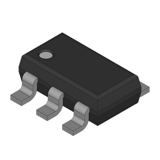
Package options are available in the 4−channel tiny 8−pad UDFN
2 mm x 2 mm with a max height of 0.55 mm, and 2 or 3− channel in
the 6−lead TSOT−23 and SC−70.
Features
•
•
•
•
•
•
•
•
•
•
UDFN−8
HU2 SUFFIX
CASE 517AW
TSOT23−6
TD SUFFIX
CASE 419AF
SC70−6
SD SUFFIX
CASE 419AD
TYPICAL APPLICATION CIRCUIT
VIN
2, 3, 4 LED Current Sinks with Tight Matching
32 Dimming Levels
Low Dropout Driver 75 mV at 20 mA
No Switching Noise
Shutdown Current less than 1 mA
25 mA Max LED Current per Channel
Dimming via 1−wire EZDimt Interface
Thermal Shutdown Protection
RoHS Compliant
6−lead TSOT−23, SC−70, and 8−pad UDFN 2 mm x 2 mm Packages
2.4 V
to
5.5 V
CIN
1 mF
LED1
LED2
VIN
CAT4002B
One Wire
Programming
32 Steps
EN/DIM
GND
Typical Applications
• LCD Display Backlight
• Cellular Phones
• Digital Still Cameras
© Semiconductor Components Industries, LLC, 2011
June, 2011 − Rev. 4
ORDERING INFORMATION
See detailed ordering information on page 2 of this data
sheet.
1
Publication Order Number:
CAT4002B/D
�CAT4002B, CAT4003B, CAT4004B
MARKING DIAGRAMS
BH
A
Y
M
BHA
YM
VKYM
VHA
UDFN8 (2 x 2 mm)
TSOT23−6L
SC70−6L
KLYM
KLA
TSOT23−6L
SC70−6L
= CAT4004B Device Code
= Assembly Location Code
= Production Year (last digit)
= Production Month: 1 − 9, O, N, D
VK
KL
Y
M
= CAT4002B Device Code
= CAT4003B Device Code
= Production Year (last digit)
= Production Month: 1 − 9, O, N, D
VH = CAT4002B Device Code
KL = CAT4003B Device Code
A
= Assembly Location Code
ORDERING INFORMATION (Note 1)
Package
Finish
Shipping (Note 2)
CAT4002BTD−GT3
TSOT−23, 6−Lead
NiPdAu (RoHS Compliant)
3,000 / Tape & Reel
CAT4002BSD−GT3
SC−70, 6−Lead
NiPdAu (RoHS Compliant)
3,000 / Tape & Reel
CAT4003BTD−GT3
TSOT−23, 6−Lead
NiPdAu (RoHS Compliant)
3,000 / Tape & Reel
CAT4003BSD−GT3
SC−70, 6−Lead
NiPdAu (RoHS Compliant)
3,000 / Tape & Reel
UDFN, 8−Pad, 2 x 2 mm
NiPdAu (RoHS Compliant)
3,000 / Tape & Reel
Orderable Part Number
CAT4004BHU2−GT3
1. For additional package and temperature options, please contact your nearest ON Semiconductor Sales office.
2. For information on tape and reel specifications, including part orientation and tape sizes, please refer to our Tape and Reel Packaging
Specifications Brochure, BRD8011/D.
http://onsemi.com
2
�CAT4002B, CAT4003B, CAT4004B
PIN CONNECTIONS (Top View)
1
1
EN/DIM
GND
LED1
LED2
VIN
NC
LED4
LED3
EN/DIM
LED1
LED1
GND
LED2
GND
VIN
LED3
EN/DIM
CAT4004B
UDFN8 2 x 2 mm
1
LED3
VIN
CAT4003B
SC70−6L
CAT4003B
TSOT23−6L
1
EN/DIM
GND
1
LED1
LED1
NC
GND
NC
EN/DIM
VIN
LED2
VIN
LED2
LED2
CAT4002B
SC70−6L
CAT4002B
TSOT23−6L
Table 1. PIN FUNCTIONS
Pin Name
Function
EN/DIM
Device Enable (active high) and Dimming Control
GND
Ground Reference
LED1
LED1 Cathode Terminal
LED2
LED2 Cathode Terminal
LED3
LED3 Cathode Terminal
LED4
LED4 Cathode Terminal
VIN
Device Supply Input, Connect to Battery or Supply
TAB
Connect to GND on the PCB, for CAT4004B only.
Table 2. ABSOLUTE MAXIMUM RATINGS
Parameter
Value
Unit
6
V
VIN + 0.7
V
Storage Temperature Range
−65 to +160
°C
Junction Temperature Range
−40 to +125
°C
300
°C
VIN, LEDx Voltage
EN/DIM Voltage
Lead Temperature
Stresses exceeding Maximum Ratings may damage the device. Maximum Ratings are stress ratings only. Functional operation above the
Recommended Operating Conditions is not implied. Extended exposure to stresses above the Recommended Operating Conditions may affect
device reliability.
Table 3. RECOMMENDED OPERATING CONDITIONS
Parameter
Value
Unit
VIN
2.4 to 5.5
V
Ambient Temperature Range
−40 to +85
°C
0 to 25
mA
LED Current Range
3. Typical application circuit with external components is shown on page 1.
http://onsemi.com
3
�CAT4002B, CAT4003B, CAT4004B
Table 4. ELECTRICAL OPERATING CHARACTERISTICS
(over recommended operating conditions unless specified otherwise) (VIN = 4.0 V, EN = High, TAMB = 25°C)
Parameter
Conditions
Symbol
Min
Typ
Max
Units
Quiescent Current
ILED = 25 mA/channel
IQ
0.5
0.7
1.5
mA
Shutdown Current
VEN = 0 V
IQSHDN
1
mA
Full Scale LED Current (Average) (Note 4)
ILED−FULL
24
25
26
mA
LED Channel Matching
I LED * I LEDAVG
I LEDAVG
ILED−DEV
−5
±1
+5
%
ILED = 20 mA
ILED = 1 mA
VDOUT
Dropout Voltage
EN/DIM Pin
− Internal pull−down resistor
− Logic High Level
− Logic Low Level
REN/DIM
VHI
VLO
75
45
mV
200
kW
V
V
1.3
0.4
Thermal Shutdown
TSD
150
°C
Thermal Hysteresis
THYS
20
°C
Undervoltage lockout (UVLO) threshold
VUVLO
2.0
V
4. For the CAT4004B, ILEDAVG = (ILED,CH1 + ILED,CH2 + ILED,CH3 + ILED,CH4) / 4
For the CAT4003B, ILEDAVG = (ILED,CH1 + ILED,CH2 + ILED,CH3) / 3
For the CAT4002B, ILEDAVG = (ILED,CH1 + ILED,CH2) / 2
5. The standard lead finish is NiPdAu.
Table 5. RECOMMENDED EN/DIM TIMING (For 2.4 V ≤ VIN ≤ 5.5 V, over full ambient temperature range −40°C to +85°C.)
Parameter
Conditions
Symbol
Min
EN/DIM program low time
TLO
0.2
EN/DIM program high time
THI
0.2
LED current settling time
TLED
EN/DIM low time to shutdown
Typ
Max
Units
100
ms
ms
10
TPWRDWN
2
3
ms
5
ms
THI
EN/DIM
TLO
TPWRDWN
TLED
100%
LED
Current
100%
97% 94%
32 Levels
Shutdown
3%
0%
Shutdown
Figure 1. CAT400XB EN/DIM Dimming Timing Diagram
LED Current Setting
On the CAT400XB, the full scale LED current is
internally set to 25 mA (no external resistor).
When the EN/DIM is first enabled, the CAT400XB sets
the LED channel current to the full scale current. Each
consecutive rising edge on the EN/DIM decreases the LED
current by one step until it goes to zero, as shown on
Figure 1.
http://onsemi.com
4
�CAT4002B, CAT4003B, CAT4004B
TYPICAL CHARACTERISTICS
(CAT4003B, VIN = 4 V, VF = 3.3 V, IOUT = 75 mA (3 LEDs at 25 mA), CIN = 1 μF, TAMB = 25°C unless otherwise specified.)
1.4
−40°C
1.2
QUIESCENT CURRENT [mA]
ENABLE HIGH THRESHOLD [V]
1.4
25°C
1.0
0.8
0.6
80°C
0.4
1.2
1.0
0.8
0.6
2.0 2.5
3.0
3.5
4.0
4.5
5.0
5.5
2.5 3.0
1.0
10
0.8
8
0.6
0.4
0.2
0.0
−0.2
−0.4
−0.6
3.5
4.0
4.5
4.5
5.0
5.5
Figure 3. Quiescent Current vs. Input Voltage
(full load)
LED CURRENT CHANGE [%]
LED CURRENT CHANGE [%]
Figure 2. EN High Threshold vs. Input Voltage
2.5 3.0
4.0
INPUT VOLTAGE [V]
INPUT VOLTAGE [V]
−0.8
−1.0
3.5
5.0
5.5
6
4
2
0
−2
−4
−6
−8
−10
−40
INPUT VOLTAGE [V]
0
40
80
120
TEMPERATURE [°C]
Figure 4. LED Current Change vs. Input Voltage
Figure 5. LED Current Change vs. Temperature
http://onsemi.com
5
�CAT4002B, CAT4003B, CAT4004B
TYPICAL CHARACTERISTICS
(CAT4003B, VIN = 4 V, VF = 3.3 V, IOUT = 75 mA (3 LEDs at 25 mA), CIN = 1 μF, TAMB = 25°C unless otherwise specified.)
30
100
25mA
90
20
EFFICIENCY [%]
LED CURRENT [mA]
25
15
10
5
0
0.8mA
0
50
100
150
200
250
80
70
60
50
300
LED PIN VOLTAGE [mV]
3.0
3.5
4.0
4.5
5.0
INPUT VOLTAGE [V]
Figure 6. Dropout Characteristics
Figure 7. Efficiency vs. Input Voltage
Figure 8. Power Up Waveform
Figure 9. Power Down Waveform
Figure 10. Line Transient Waveform
Figure 11. Dimming Levels
http://onsemi.com
6
�CAT4002B, CAT4003B, CAT4004B
Pin Functions
into “zero current” shutdown mode, the EN/DIM pin must
be held low for 3 ms typical
LED1 to LED4 provide the internal regulated current for
each of the LED cathodes. The pins enter a high impedance
zero current state whenever the device is placed in shutdown
mode.
GND is the ground reference for the device. The pin must be
connected to the ground plane on the PCB.
TAB (CAT4004B only) is the exposed pad underneath the
package. For best thermal performance, the tab should be
soldered to the PCB and connected to the ground plane.
VIN is the supply pin for the charge pump. A small 1 mF
ceramic bypass capacitor is required between the VIN pin
and ground near the device. The operating input voltage
range is from 2.4 V to 5.5 V. Whenever the input supply falls
below the under−voltage threshold (2.0 V), all the LED
channels are disabled and the device enters shutdown mode.
EN/DIM is the enable and one wire dimming input for all
LED channels. Levels of logic high and logic low are set at
1.3 V and 0.4 V respectively. When EN/DIM is initially
taken high, the CAT400XB becomes enabled and all LED
currents are set to the full scale 25 mA. To place the device
LED4
LED3
Undervoltage
Lockout
VIN
LED2
LED1
VIN
Reference
Voltage
Current
Setting DAC
EN/DIM
Serial
Interface
4 Current Sink
Regulators
Register
200 kΩ
GND
Figure 12. CAT4004B Functional Block Diagram
Basic Operation
The full scale current is calculated from the above formula
with n equal to zero.
The EN/DIM pin has two primary functions. One function
enables and disables the device. The other function is LED
current dimming with 32 different levels by pulsing the input
signal, as shown on Figure 13. On each consecutive pulse
rising edge, the LED current is decreased by about 3.2%
(1/31th of the full scale value). After 30 pulses, the LED
current is 3.2% of the full scale current. On the 31st pulse, the
current drops to zero, and then goes back to full scale on the
following pulse.
Each pulse width should be between 200 ns and 100 ms.
Pulses faster than the minimum TLO may be ignored and
filtered by the device. Pulses longer than the maximum TLO
may shutdown the device. By pulsing the EN/DIM signal at
high frequency, the LED current can quickly be set to zero.
The LED driver enters a “zero current” shutdown mode if
EN/DIM is held low for 3 ms typical.
The dimming level is set by the number of pulses on the
EN/DIM after the power−up, as shown in Table 6.
The CAT400XB uses tightly matched current sinks to
accurately regulate LED current in each channel.
There are 32 different settings for LED brightness that can
be programmed through the EN/DIM pin. Tight current
regulation for all channels is possible over a wide range of
input and LED voltages due to independent current sensing
circuitry on each channel.
Each LED channel needs a minimum of 75 mV headroom
to sink a constant regulated current of 20 mA. If the input
supply falls below 2.0 V, the under−voltage lockout circuit
disables all LED channels and resets the circuit to default
values. Any unused LED channels should be left open.
CAT400XB LED Current Selection
After power−up and once enabled, the LED current is set
initially to the full scale currrent of 25 mA. The number of
pulses (n) on the EN/DIM input does decrease the current
value as follows:
LED current [mA] + 25
ǒ3131* nǓ
http://onsemi.com
7
�CAT4002B, CAT4003B, CAT4004B
Table 6. DIMMING LEVELS
Full Scale Current in %
Dimming Pulses [n]
Full Scale Current in %
Dimming Pulses [n]
48
16
100
0
45
17
97
1
42
18
94
2
39
19
90
3
35
20
87
4
32
21
84
5
29
22
81
6
26
23
77
7
23
24
74
8
19
25
71
9
16
26
68
10
13
27
65
11
10
28
61
12
6
29
58
13
3
30
55
14
0
31
52
15
100
32
THI
EN/DIM
TLO
TPWRDWN
TLED
100%
LED
Current
Shutdown
100%
97% 94%
32 Levels
3%
0%
Figure 13. EN/DIM Digital Dimming Timing Diagram
http://onsemi.com
8
Shutdown
�CAT4002B, CAT4003B, CAT4004B
PACKAGE DIMENSIONS
UDFN8, 2x2
CASE 517AW−01
ISSUE O
D
A
D2
DETAIL A
E
E2
PIN #1
IDENTIFICATION
A1
PIN #1 INDEX AREA
TOP VIEW
SIDE VIEW
SYMBOL
MIN
NOM
MAX
A
0.45
0.50
0.55
A1
0.00
0.02
0.05
b
0.18
0.25
0.30
D
1.90
2.00
2.10
D2
1.50
1.60
1.70
E
1.90
2.00
2.10
E2
0.80
0.90
1.00
e
L
BOTTOM VIEW
b
L
e
0.50 BSC
0.20
0.30
DETAIL A
0.45
Notes:
(1) All dimensions are in millimeters.
(2) Complies with JEDEC MO-229.
http://onsemi.com
9
�CAT4002B, CAT4003B, CAT4004B
PACKAGE DIMENSIONS
SC−70, 6 Lead, 1.25x2
CASE 419AD−01
ISSUE O
D
e
e
E1 E
SYMBOL
MIN
A
0.80
MAX
1.10
A1
0.00
0.10
A2
0.80
1.00
b
0.15
0.30
c
0.10
0.18
D
1.80
2.00
2.20
E
1.80
2.10
2.40
E1
1.15
1.25
1.35
e
L
0.65 BSC
0.26
0.36
0.46
0.42 REF
L1
L2
TOP VIEW
NOM
0.15 BSC
θ
0º
8º
θ1
4º
10º
q1
A2 A
q
q1
b
L
L1
A1
SIDE VIEW
c
END VIEW
Notes:
(1) All dimensions are in millimeters. Angles in degrees.
(2) Complies with JEDEC MO-203.
http://onsemi.com
10
L2
�CAT4002B, CAT4003B, CAT4004B
PACKAGE DIMENSIONS
TSOT−23, 6 LEAD
CASE 419AF−01
ISSUE O
SYMBOL
D
MIN
NOM
A
e
E1
MAX
1.00
A1
0.01
0.05
0.10
A2
0.80
0.87
0.90
b
0.30
c
0.12
0.45
0.15
D
2.90 BSC
E
2.80 BSC
E1
1.60 BSC
E
e
0.20
0.95 TYP
L
0.30
0.40
L1
0.60 REF
L2
0.25 BSC
0º
θ
0.50
8º
TOP VIEW
A2 A
b
q
L
A1
c
L2
L1
SIDE VIEW
END VIEW
Notes:
(1) All dimensions are in millimeters. Angles in degrees.
(2) Complies with JEDEC MO-193.
ON Semiconductor and
are registered trademarks of Semiconductor Components Industries, LLC (SCILLC). SCILLC reserves the right to make changes without further notice
to any products herein. SCILLC makes no warranty, representation or guarantee regarding the suitability of its products for any particular purpose, nor does SCILLC assume any liability
arising out of the application or use of any product or circuit, and specifically disclaims any and all liability, including without limitation special, consequential or incidental damages.
“Typical” parameters which may be provided in SCILLC data sheets and/or specifications can and do vary in different applications and actual performance may vary over time. All
operating parameters, including “Typicals” must be validated for each customer application by customer’s technical experts. SCILLC does not convey any license under its patent rights
nor the rights of others. SCILLC products are not designed, intended, or authorized for use as components in systems intended for surgical implant into the body, or other applications
intended to support or sustain life, or for any other application in which the failure of the SCILLC product could create a situation where personal injury or death may occur. Should
Buyer purchase or use SCILLC products for any such unintended or unauthorized application, Buyer shall indemnify and hold SCILLC and its officers, employees, subsidiaries, affiliates,
and distributors harmless against all claims, costs, damages, and expenses, and reasonable attorney fees arising out of, directly or indirectly, any claim of personal injury or death
associated with such unintended or unauthorized use, even if such claim alleges that SCILLC was negligent regarding the design or manufacture of the part. SCILLC is an Equal
Opportunity/Affirmative Action Employer. This literature is subject to all applicable copyright laws and is not for resale in any manner.
PUBLICATION ORDERING INFORMATION
LITERATURE FULFILLMENT:
Literature Distribution Center for ON Semiconductor
P.O. Box 5163, Denver, Colorado 80217 USA
Phone: 303−675−2175 or 800−344−3860 Toll Free USA/Canada
Fax: 303−675−2176 or 800−344−3867 Toll Free USA/Canada
Email: orderlit@onsemi.com
N. American Technical Support: 800−282−9855 Toll Free
USA/Canada
Europe, Middle East and Africa Technical Support:
Phone: 421 33 790 2910
Japan Customer Focus Center
Phone: 81−3−5773−3850
http://onsemi.com
11
ON Semiconductor Website: www.onsemi.com
Order Literature: http://www.onsemi.com/orderlit
For additional information, please contact your local
Sales Representative
CAT4002B/D
�


 工商网监
湘ICP备2023018690号
工商网监
湘ICP备2023018690号
