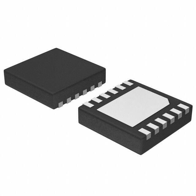
CAT4134
LED Driver, Dual Channel
Movie/Flash, 500 mA
Description
The CAT4134 is a high power, dual channel boost converter which
provides two matched LED currents. Output current levels are
controlled by one of two resistors RSET or RFLASH. When the
FLASH input pin is low (movie mode), RSET sets the current. When
FLASH is high (flash mode), the resistor RFLASH sets the LED
current. Each channel drives two or three white LEDs in series and
provides a regulated current to control their brightness. Input supply
down to 3 V is supported, making the device ideal for Li−Ion battery
applications.
High frequency low noise operation allows the device to be used
with small external inductors and ceramic capacitors while still
maintaining excellent efficiency. When not in use the device can be
placed into a “zero” quiescent mode via the shutdown pin.
In addition to soft-start control and current limiting, the CAT4134
include thermal shutdown protection. A dedicated overvoltage pin
(OVP) allows the user to limit the maximum LED supply voltage. The
device is packaged in the 12−pad TDFN 3 mm x 3 mm.
Features
•
•
•
•
•
•
•
•
•
•
•
•
Dual Mode (Movie or Flash) Operation
Independent Movie/Flash LED Current Control
Can Drive 2, 3, 4 or 6 LEDs
High LED Current (250 mA Max per Channel)
Power Efficiency up to 85%
Dual Frequency Mode 1.2 MHz and 900 kHz
Soft−start Inrush Current
Adjustable Overvoltage Protection
Thermal Shutdown Protection
Operating Temperature Range −40°C to +85°C
12−pad TDFN 3 mm x 3 mm Package
These Devices are Pb−Free, Halogen Free/BFR Free and are RoHS
Compliant
Applications
•
•
•
•
•
Camera Flash
Flash Light
High−power White LEDs
Digital Still Cameras
Color LCD Backlighting
© Semiconductor Components Industries, LLC, 2010
February, 2010 − Rev. 2
http://onsemi.com
TDFN−12
HV2 SUFFIX
CASE 511AN
PIN CONNECTIONS
1
FLASH
EN
OVP
SW
TAB
is
GND
PGND
AGND
SW
VIN
LED2
RSET
LED1
RFLASH
(Top View)
MARKING DIAGRAM
HAAS
HAAU
HAAS = CAT4134HV2−T2
HAAU = CAT4134HV2−GT2
ORDERING INFORMATION
Device
Package
Shipping
CAT4134HV2−T2
(Note 1)
TDFN−12
(Pb−Free)
2,000/
Tape & Reel
CAT4134HV2−GT2
(Note 2)
TDFN−12
(Pb−Free)
2,000/
Tape & Reel
1. Matte−Tin Plated Finish (RoHS−compliant).
2. NiPdAu Plated Finish (RoHS−compliant)
1
Publication Order Number:
CAT4134/D
�CAT4134
D
L
VIN
3 V to 4.2 V
22 mH
C1
VOUT
C2
10 mF
10 mF
SW
VIN
R1
1 MW
EN
CAT4134
FLASH
LED1
RFLASH LED2
RSET
OVP
OFF ON
RFLASH
18 kW
RSET
20 kW
AGND
PGND
L = Sumida CDRH3D16−220
D = Central CMDSH05−4 (500 mA)
C2 = 10 mF (rated 16 V)
R2
100 kW
Figure 1. Typical Application Circuit
Table 1. ABSOLUTE MAXIMUM RATINGS
Parameters
Ratings
Units
SW voltage
20
V
VIN voltage
8
V
VIN + 0.6 V
V
8
V
Output Current per Channel
300
mA
Storage Temperature Range
−65 to +160
_C
Junction Temperature Range
−40 to +125
_C
300
_C
2,000
V
EN, FLASH, RSET, RFLASH voltage
LED1, LED2 voltage
Lead Temperature
ESD Rating − Human Body Model (HBM)
Stresses exceeding Maximum Ratings may damage the device. Maximum Ratings are stress ratings only. Functional operation above the
Recommended Operating Conditions is not implied. Extended exposure to stresses above the Recommended Operating Conditions may affect
device reliability.
Table 2. RECOMMENDED OPERATING CONDITIONS
Parameters
Range
Units
VIN
2.8 to 4.2
V
Ambient Temperature Range
−40 to +85
_C
Flash mode current per channel
25 to 250
mA
Movie mode current per channel
5 to 50
mA
http://onsemi.com
2
�CAT4134
Table 3. ELECTRICAL OPERATING CHARACTERISTICS
(VIN = 3.6 V, EN = VIN and at ambient temperature of 25°C (over recommended operating conditions unless otherwise specified))
Symbol
Parameter
Conditions
IQ
Quiescent Current (not switching)
VLED1 > 0.5 V, VLED2 > 0.5 V
ISD
Shutdown Current
EN = 0 V
ISW
Switch Current Limit
Movie Mode (FLASH = Low)
Flash Mode (FLASH = High)
RSW
Switch Resistance
ISW = 1000 mA
Switch Leakage Current
Switch Off, VSW = 5 V
FOSC
Oscillator Frequency
Movie Mode
Flash Mode
VOVP
OVP pin threshold
ILK
0.5
1.7
Typ
Max
Unit
100
250
mA
1
mA
1
2
A
0.3
0.5
W
5
mA
1.2
0.9
1.10
VOUT = 10 V, Load = 200 mA
1.20
MHz
1.30
V
85
%
TSD
Thermal Shutdown
150
°C
THYST
Thermal Hysteresis
20
°C
VUVLO
Undervoltage Lock Out (UVLO) Threshold
h
Efficiency
Min
Disabled when VIN < VUVLO
1.9
2.2
V
0.7
0.7
1.5
V
10
40
mA
EN LOGIC CONTROL INPUT
VSDHI
VSDLO
Logic High Threshold
Logic Low Threshold
EN > VSDHI Enables Device
ISDBIAS
Input Bias current
EN = 3 V
VRSET
RSET pin voltage
22 kW < RSET < 200 kW
1.10
1.20
1.30
V
RFLASH pin voltage
22 kW < RFLASH < 200 kW
1.10
1.20
1.30
V
VLED
LED1, LED2 Pin Voltage
(whichever is the lower)
Both Flash and Movie Mode
(lower voltage pin is regulated)
400
mV
ILED
Programmed LED Current
RSET = 21.6 kW
RFLASH = 43.2 kW
RFLASH = 21.6 kW
20
50
100
mA
ILED-RAN
LED Current Adjust Range per LED output
In Movie mode
In Flash mode
ILED-ACC
LED Current Accuracy
±5
%
ILED-DEV
LED Current Matching
±5
%
VRFLASH
0.4
5
25
50
200
mA
FLASH CONTROL LOGIC INPUT
VFHI
VFLO
Logic High Threshold
Logic Low Threshold
FLASH > VFHI Flash Enabled
IINPUT
Input Bias current
FLASH = 3 V
0.4
http://onsemi.com
3
0.7
0.7
1.5
V
10
40
mA
�CAT4134
TYPICAL CHARACTERISTICS
2.0
2.0
1.5
1.5
LED CURRENT CHANGE (%)
LED CURRENT CHANGE (%)
(VIN = 3.6 V, FLASH = VIN, CIN = 4.7 mF, COUT = 10 mF, L = 22 mH with 2 LEDs at 100 mA, TAMB = 25°C, unless otherwise specified.)
1.0
0.5
1 LED
0
2 LEDs
−0.5
−1.0
−1.5
−2.0
2.5
3.0
3.5
4.0
0
−1.0
−1.5
2.5
3.0
3.5
4.0
INPUT VOLTAGE (V)
Figure 2. LED Current Regulation
(100 mA Load)
Figure 3. LED Current Regulation
(200 mA Load, Flash)
4.5
2.0
LED CURRENT CHANGE (%)
2 LEDs
VIN = 3.6 V
1850
1800
1750
1700
1650
0
50
100
150
1.5
0.5
0
−0.5
−1.0
−1.5
−2.0
200
2.5
3.0
3.5
4.0
Rflash (kW)
INPUT VOLTAGE (V)
Figure 4. Current Gain vs. RFLASH
Figure 5. LED Current Regulation
(100 mA Load, Flash)
90
80
80
70
2 LEDs
VIN = 3.6 V
60
2 LEDs at 100 mA
1.0
90
4.5
70
60
2 LEDs at 100 mA
50
50
40
2 LEDs
−0.5
INPUT VOLTAGE (V)
EFFICIENCY (%)
CURRENT GAIN (Iout / Iflash)
EFFICIENCY (%)
0.5
−2.0
4.5
1900
1600
1.0
0
50
100
150
200
40
250
2.5
3.0
3.5
4.0
4.5
TOTAL LED CURRENT (mA)
INPUT VOLTAGE (V)
Figure 6. Efficiency vs. Output Current
(Flash Mode)
Figure 7. Efficiency vs. Input Voltage
(Flash Mode)
http://onsemi.com
4
5.0
�CAT4134
TYPICAL CHARACTERISTICS
(VIN = 3.6 V, FLASH = VIN, CIN = 4.7 mF, COUT = 10 mF, L = 22 mH with 2 LEDs at 100 mA, TAMB = 25°C, unless otherwise specified.)
Figure 8. Power−up Transient
(2 LEDs at 200 mA)
Figure 9. Power−up Transient
(2 LEDs at 200 mA)
Figure 10. Power−up Transient
(2 LEDs at 200 mA)
Figure 11. Power−up Transient
(2 LEDs at 200 mA)
Figure 12. Switching Waveform in Flash Mode
(2 LEDs)
http://onsemi.com
5
�CAT4134
TYPICAL CHARACTERISTICS
(VIN = 3.6 V, CIN = 4.7 mF, COUT = 10 mF, L = 22 mH with 2 LEDs at 100 mA, TAMB = 25°C, unless otherwise specified.)
CLOCK FREQUENCY (kHz)
1300
Movie Mode
20 mA per LED
1200
1100
1000
Flash Mode
50 mA per LED
900
800
2.5
3.0
3.5
4.0
4.5
INPUT VOLTAGE (V)
Figure 13. Switching Frequency vs.
Supply Voltage
Figure 14. Enable Flash Waveform
http://onsemi.com
6
�CAT4134
Table 4. PIN DESCRIPTION
Pin #
Name
Function
1
FLASH
2
EN
3
PGND
Power ground reference.
4
AGND
Analog ground reference.
5
LED2
LED channel 2, connected to the LED cathode.*
6
LED1
LED channel 1, connected to the LED cathode.*
7
RFLASH
Resistor connection to set Flash mode LED current.
8
RSET
Resistor connection to set Movie mode LED current.
9
VIN
Power supply input.
10, 11
SW
Drain connection of low resistance power MOSFET.
12
OVP
Over Voltage Protection comparator input
Logic input, set high to select the flash mode.
Enable control logic input (Active High).
*LED1 or LED2 pin should not be left floating.
Pin Function
VIN is the supply voltage input. The device is compatible
with supply voltages down to 2.8 V and up to 4.2 V. Internal
under-voltage lockout (UVLO) circuitry will automatically
prevent the device from operating whenever the supply falls
below 1.9 V. For operation up to maximum rated loads a
bypass ceramic capacitor of 10 mF is recommended between
the VIN and GND pins near the device.
EN is the enable logic input (active high). When the pin
voltage is taken below 0.4 V, the device enters shutdown
mode, drawing nearly zero current. At pin voltages greater
than 1.4 V, the device is fully enabled.
FLASH is the logic input (active high) used to control Flash
mode operation. When the pin voltage is taken above 1.4 V,
the device transitions from Movie mode to Flash mode.
When the pin voltage is taken back below 0.4 V, the device
returns back to Movie mode operation.
RSET, RFLASH pins allow to set the LED current
respectively in Movie and Flash mode. These pins, regulated
at 1.2 V, must be connected to a pull-down resistor tied to
ground. The LED current is a function of the resistor value.
GND is the ground reference for the driver. The pin must be
connected to the ground plane on the PCB.
SW pin is the drain terminal of the internal low resistance
power switch. The inductor and the Schottky diode anode
should be connected to the SW pin. Traces going to the SW
pin should be as short as possible with minimum loop area.
This pin contains over-voltage circuitry which becomes
active above 18 V. In the event of an “open-LED” fault
condition, the device will enter a low power mode and the
SW pin will be clamped to approximately 21 V.
LED1, LED2 provide the internal regulated current for each
of the LED cathodes. These pins enter a high impedance
zero current state whenever the device is placed in shutdown
mode. In applications with only one string of LEDs, the two
LED pins should be tied together. LED pins should not be
left floating.
OVP is the overvoltage protection input pin. When the pin
voltage exceeds the 1.2 V overvoltage threshold (VOVP), the
driver stops switching. The output VOUT then drops down.
As soon as the OVP pin voltage falls under the VOVP
threshold, the part starts switching again.
TAB is the exposed pad underneath the package. For best
thermal performance, the tab should be soldered to the PCB
and connected to the ground plane.
http://onsemi.com
7
�CAT4134
Device Operation
The device is powered from the input pin VIN. A
switching frequency of 1.2 MHz is used in Movie mode,
when the FLASH input is low. Continuous LED current up
to 50 mA is controlled by the RSET resistor. For higher load
current, the Flash mode is selected by setting the FLASH
input pin high. RFLASH now controls the LED current. In
flash mode, the driver efficiency is kept high even under
high load current by using a lower switching frequency of
900 kHz. In movie mode, the higher frequency of 1.2 MHz
provides a lower noise operation.
maximum operating voltage on the output VOUT using
external resistors R1 and R2. The resistor ratio sets the
maximum output voltage as shown in the equation below:
ǒ
Ǔ
R1 + VOUT MAX * 1.2
1.2
R2
VOUTMAX should always be higher than the total LED
forward voltage (SVf) plus 1.2 V. Also VOUT must be less
than SVf + 8 V.
SVf ) 1.2 V t VOUT MAX t SVf ) 8 V t 16 V
Overvoltage Protection (OVP)
If the overvoltage protection is not needed, then the OVP pin
should be connected to Ground. In that case, the maximum
voltage on the SW pin is set to 17 V.
To prevent the SW pin voltage from exceeding the internal
switch maximum voltage rating, an overvoltage protection
(OVP) function is supported. The OVP pin allows to set the
Block Diagram
VOUT
VIN
CIN
COUT
SW
VIN
Dual
Frequency
PWM
Controller
EN
PGND
LED1
FLASH
LED2
OVP
RFLASH
RSET
RFLASH
R1
mux
Current
Setting
2 Current Sink
Regulators
RSET
AGND
Figure 15. Block Diagram
http://onsemi.com
8
R2
�CAT4134
Application Information
Movie Mode
When the EN input is high and FLASH is low, the driver
is in movie mode. In this mode, the LED1 and LED2 pin
currents are set by the resistor RSET and are regulated to 360
times the current in the RSET resistor and follows the
equation:
The typical application for the CAT4134 is in a
camera−equipped cellular phone where the LEDs are used
for illumination in flash mode with short duration
high−current pulse and in movie mode with continuous
lighter load. In movie mode, the FLASH pin is set low.
NOTE:
Hot-plugging the LEDs while the output is fully charged
is not recommended. If the LEDs are disconnected, the
device should first be powered-down and the output
discharged before reconnecting the LEDs to the output
and the LED pins.
LED current + 360
1.2 V
RSET
Table 5 lists the various LED currents and the associated
resistor values in movie and flash modes.
Table 5.
RESISTOR SELECTION IN MOVIE AND FLASH MODE
EN
LED1, LED2
Current
Flash Mode
Movie Mode
FLASH
LED Current
(mA)
movie
mode
flash
mode
movie
mode
Figure 16. Timing Diagram
RSET
(kW)
LED Current
(mA)
RFLASH
(kW)
5
86.4
50
43.2
10
43.2
75
28.8
20
21.6
100
21.6
30
14.4
150
14.4
LED Current Setting
Shutdown Mode
Flash Mode
When the EN input is low, the driver is in shutdown mode
and there is no current flowing in either LED1 or LED2 pins.
The enable EN and FLASH logic input signals control the
LED current. When both the EN and FLASH inputs are high,
the driver is in flash or strobe mode. In this mode, the LED1
and LED2 pin currents are set by the resistor RFLASH and
are regulated to 1800 times the current in the RFLASH
resistor and follows the equation:
LED current + 1800
1.2 V
RFLASH
http://onsemi.com
9
�CAT4134
Typical Applications
The CAT4134 can drive one or two strings of 2 to 3 LEDs
in series resulting in combinations of 2, 3, 4, 6 LEDs.
The resistor ratio R1/R2 sets the maximum VOUT during
an open-LED fault condition and provides the overvoltage
protection.
For applications with 2 LEDs in series and VOUTMAX at
10 V, the ratio R1/R2 is 7.
For applications with 3 LEDs in series and VOUTMAX at
13.5 V, the ratio R1/R2 is 10.
Figure 17. 2 LED Application
Figure 18. 3 LED Application
Figure 19. 4 LED Application
Figure 20. 6 LED Application
http://onsemi.com
10
�CAT4134
Example of Ordering Information (Note 5)
3.
4.
5.
6.
7.
Prefix
Device #
Suffix
CAT
4134
HV2
−G
T2
Company ID
(Optional)
Product Number
4134
Package
HV2: TDFN
Lead Finish
Blank: Matte−Tin
G: NiPdAu
Tape & Reel (Note 7)
T: Tape & Reel
2: 2,000 / Reel
All packages are RoHS−compliant (Lead−free, Halogen−free).
The standard lead finish is NiPdAu.
The device used in the above example is a CAT4134HV2−GT2 (TDFN, NiPdAu, Tape & Reel, 2,000/Reel).
For additional package and temperature options, please contact your nearest ON Semiconductor Sales office.
For information on tape and reel specifications, including part orientation and tape sizes, please refer to our Tape and Reel Packaging
Specifications Brochure, BRD8011/D.
http://onsemi.com
11
�MECHANICAL CASE OUTLINE
PACKAGE DIMENSIONS
TDFN12, 3x3
CASE 511AN−01
ISSUE A
D
DATE 18 MAR 2009
A
e
b
L
E
E2
PIN#1 ID
PIN#1 INDEX AREA
A1
TOP VIEW
BOTTOM VIEW
SIDE VIEW
SYMBOL
MIN
NOM
MAX
A
0.70
0.75
0.80
A1
0.00
0.02
0.05
A3
0.178
0.203
0.228
b
0.18
0.23
0.30
D
2.90
3.00
3.10
D2
2.30
2.40
2.50
E
2.90
3.00
3.10
E2
1.55
1.70
1.75
e
D2
A
A3
A1
FRONT VIEW
RECOMMENDED LAND PATTERN
R
e
M
0.45 BSC
L
0.30
0.40
0.50
M
0.25
0.30
0.35
N
0.60
0.70
0.80
P
2.70
3.00
3.10
R
2.25 TYP
N
P
E2
Notes:
(1) All dimensions are in millimeters.
(2) Complies with JEDEC MO-229.
D2
DOCUMENT NUMBER:
DESCRIPTION:
98AON34357E
TDFN12, 3X3
Electronic versions are uncontrolled except when accessed directly from the Document Repository.
Printed versions are uncontrolled except when stamped “CONTROLLED COPY” in red.
PAGE 1 OF 1
ON Semiconductor and
are trademarks of Semiconductor Components Industries, LLC dba ON Semiconductor or its subsidiaries in the United States and/or other countries.
ON Semiconductor reserves the right to make changes without further notice to any products herein. ON Semiconductor makes no warranty, representation or guarantee regarding
the suitability of its products for any particular purpose, nor does ON Semiconductor assume any liability arising out of the application or use of any product or circuit, and specifically
disclaims any and all liability, including without limitation special, consequential or incidental damages. ON Semiconductor does not convey any license under its patent rights nor the
rights of others.
© Semiconductor Components Industries, LLC, 2019
www.onsemi.com
�onsemi,
, and other names, marks, and brands are registered and/or common law trademarks of Semiconductor Components Industries, LLC dba “onsemi” or its affiliates
and/or subsidiaries in the United States and/or other countries. onsemi owns the rights to a number of patents, trademarks, copyrights, trade secrets, and other intellectual property.
A listing of onsemi’s product/patent coverage may be accessed at www.onsemi.com/site/pdf/Patent−Marking.pdf. onsemi reserves the right to make changes at any time to any
products or information herein, without notice. The information herein is provided “as−is” and onsemi makes no warranty, representation or guarantee regarding the accuracy of the
information, product features, availability, functionality, or suitability of its products for any particular purpose, nor does onsemi assume any liability arising out of the application or use
of any product or circuit, and specifically disclaims any and all liability, including without limitation special, consequential or incidental damages. Buyer is responsible for its products
and applications using onsemi products, including compliance with all laws, regulations and safety requirements or standards, regardless of any support or applications information
provided by onsemi. “Typical” parameters which may be provided in onsemi data sheets and/or specifications can and do vary in different applications and actual performance may
vary over time. All operating parameters, including “Typicals” must be validated for each customer application by customer’s technical experts. onsemi does not convey any license
under any of its intellectual property rights nor the rights of others. onsemi products are not designed, intended, or authorized for use as a critical component in life support systems
or any FDA Class 3 medical devices or medical devices with a same or similar classification in a foreign jurisdiction or any devices intended for implantation in the human body. Should
Buyer purchase or use onsemi products for any such unintended or unauthorized application, Buyer shall indemnify and hold onsemi and its officers, employees, subsidiaries, affiliates,
and distributors harmless against all claims, costs, damages, and expenses, and reasonable attorney fees arising out of, directly or indirectly, any claim of personal injury or death
associated with such unintended or unauthorized use, even if such claim alleges that onsemi was negligent regarding the design or manufacture of the part. onsemi is an Equal
Opportunity/Affirmative Action Employer. This literature is subject to all applicable copyright laws and is not for resale in any manner.
PUBLICATION ORDERING INFORMATION
LITERATURE FULFILLMENT:
Email Requests to: orderlit@onsemi.com
onsemi Website: www.onsemi.com
◊
TECHNICAL SUPPORT
North American Technical Support:
Voice Mail: 1 800−282−9855 Toll Free USA/Canada
Phone: 011 421 33 790 2910
Europe, Middle East and Africa Technical Support:
Phone: 00421 33 790 2910
For additional information, please contact your local Sales Representative
�