CAT5126
One‐time Digital 32‐tap
Potentiometer (POT)
Description
The CAT5126 is a digital POT. The wiper position is controlled with
a simple 2-wire digital interface. This digital potentiometer is unique
in that it has an optional one-time programmable feature that either
sets the wiper’s position upon power-on to a user-defined value, or the
wiper can be set and the interface also disabled to prevent further
adjustment.
The CAT5126 has an end-to-end resistance of 10 kW, 50 kW, and
100 kW. All CAT5126 devices have 32-wiper positions and operate
from a single 2.5 V to 5.5 V supply.
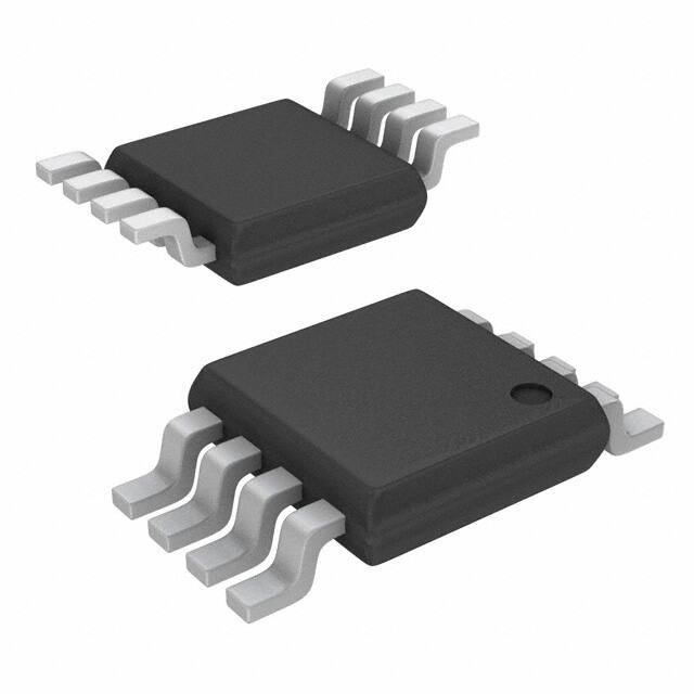
The CAT5126 is available in TDFN 8-pad and MSOP 8-lead
packages. Each device is guaranteed over the industrial temperature
range of −40C to +85C.
Wiper Position Stored after One-time Non-volatile Programming
User-defined Power-On Wiper Position
32-tap Positions
Wiper Position Programmed through Simple 2-wire Serial Interface
Low 0.35 mA (typ) Static Supply Current
2.5 V to 5.5 V Single-supply Operation
10 kW, 50 kW, and 100 kW End-to-End Resistances
50 ppm/C End-to-End Temperature Coefficient and 5 ppm/C
Ratiometric Temperature Coefficient
TDFN 8-pad (2 3 mm) and MSOP 8-lead Packages
These Devices are Pb-Free, Halogen Free/BFR Free and are RoHS
Compliant
TDFN−8
VP2 SUFFIX
CASE 511AK
PIN CONFIGURATIONS
RW
CS
VDD
GND
RH
RL
U/D
VPP
MSOP (Z)
RW
CS
VDD
GND
1
RH
RL
U/D
VPP
TDFN (VP2)
(Top Views)
ORDERING INFORMATION
See detailed ordering and shipping information in the package
dimensions section on page 9 of this data sheet.
Applications
MSOP−8
Z SUFFIX
CASE 846AD
1
Features
http://onsemi.com
Mechanical Potentiometer Replacement
Products using One-time Factory Calibration
Contrast, Brightness, Volume Controls
Programmable Analog Functions
Semiconductor Components Industries, LLC, 2013
June, 2013 − Rev. 4
1
Publication Order Number:
CAT5126/D
�CAT5126
RH
VDD
GND
CS
U/D
8
3
R31
4
2
UP/DOWN
COUNTER
R30
6
RW
32−POSITION
DECODER
VPP
5
ONE−TIME
PROGRAM
BLOCK
1
RW
R2
R1
RL
7
Figure 1. Functional Diagram
Table 1. PIN DESCRIPTION
Pin
Name
Function
1
RW
Wiper Connection
2
CS
Chip-Select Input. A high-to-low CS transition determines the mode: increment if U/D is high, or decrement if
U/D is low. CS is also used for one-time programming (see the One-Time Programming section).
3
VDD
Power−Supply Voltage
4
GND
Ground
5
VPP
Programming Voltage for One-Time Programming. Connect VPP to 10 V supply when one-time programming
the device. For normal operation, connect to ground or let float.
6
U/D
Up/Down Control Input. With CS low, a low-to-high transition increments or decrements the wiper position.
7
RL
Low Terminal of Resistor
8
RH
High Terminal of Resistor
Table 2. ABSOLUTE MAXIMUM RATINGS
Parameters
Ratings
Units
VDD to GND
−0.5 to +7.0
V
VPP to GND
−0.5 to +12.0
V
All other pins to GND
−0.5 to VDD +0.5
V
Maximum Continuous Current into H, L, and W
1.5
mA
Continuous Power Dissipation (TA = +70C)
MSOP 8-lead (derate 4.5 mW/C above +70C)
TDFN 8-pad (derate 24.4 mW/C above +70C)
362
1951
Operating Temperature Range
Junction Temperature
Storage Temperature Range
Lead Temperature (soldering, 10 s)
mW
−40 to +85
C
+150
C
−65 to +150
C
+300
C
Stresses exceeding Maximum Ratings may damage the device. Maximum Ratings are stress ratings only. Functional operation above the
Recommended Operating Conditions is not implied. Extended exposure to stresses above the Recommended Operating Conditions may affect
device reliability.
http://onsemi.com
2
�CAT5126
Table 3. ELECTRICAL CHARACTERISTICS (VDD = 2.5 V to 5.5 V, VPP = GND, RH = VDD, RL = GND, TA = −40C to +85C,
unless otherwise noted. Typical values are at VDD = 5.0 V, TA = +25C, unless otherwise noted.) (Note 1)
Symbol
Parameter
Conditions
Min
Typ
Max
Units
DC PERFORMANCE
RES
Resolution
RPOT
End−to−End Resistance
TCRPOT
TC of Pot Resistance
TCRATIO
Ratiometric Resistance TC
3.2
%
−10 Device
8
10
12
kW
−50 Device
40
50
60
−00 Device
80
100
120
50
300
ppm/C
5
20
ppm/C
INL
Integral Nonlinearity
Potentiometer configuration, no load
0.5
1
LSB
DNL
Differential Nonlinearity
Potentiometer configuration, no load
0.25
0.5
LSB
RW
Wiper Resistance
VDD = 5 V
70
100
W
VDD = 2.5 V
150
200
DIGITAL INPUTS (CS, U/D)
VIH
Input High Voltage
VIL
Input Low Voltage
IIN
Input Leakage Current
CIN
Input Capacitance
0.7 x VDD
V
0.1
0.3 x VDD
V
1
mA
5
pF
POWER SUPPLY
VDD
Supply Voltage
IDD
Stand by Current
IDDW
Programming Current
VPP
Programming Voltage
IPP
VPP Input Current
2.5
(Note 2)
5.5
V
0.35
1
mA
0.25
1
mA
VDD = 5 V
8.5
10
V
VDD = 2.5 V
6.0
10
VPP = 10 V
5
mA
TIMING CHARACTERISTICS (Note 3)
tCU
U/D Mode to CS Setup
Figures 6, 7
50
ns
tCI
CS Hold to U/D Mode
Figures 6, 7
50
ns
tIC
U/D Step Hold to CS
Figures 6, 7
0
ns
tIL
U/D Step Low Time
Figures 6, 7
100
ns
tIH
U/D Step High Time
Figures 6, 7
100
ns
tIW
Wiper Switching Time
CL = 0 pF, Figures 6, 7
tPC
VPP Rising Edge to CS
Falling Edge
Figure 8
1
ms
tCP
CS Falling Edge to VPP
Falling Edge
Figure 8
5
ms
tCL
CS Step Low Time
Figure 8
5
ms
tCH
CS Step High Time
Figure 8
5
ms
tPH
VPP Falling Edge to CS
Rising Edge
Figure 8
1
ms
fU/DMAX
1.
2.
3.
4.
U/D Frequency
100
ns
5
All devices are production tested at TA = +25C and are guaranteed by design for TA = −40C to +85C.
Digital inputs CS and U/D are connected to GND or VDD.
Digital timing is guaranteed by design, not production tested.
Power-up time is the period of time from when the power supply is applied until the serial interface is ready for writing.
http://onsemi.com
3
MHz
�CAT5126
Table 3. ELECTRICAL CHARACTERISTICS (VDD = 2.5 V to 5.5 V, VPP = GND, RH = VDD, RL = GND, TA = −40C to +85C,
unless otherwise noted. Typical values are at VDD = 5.0 V, TA = +25C, unless otherwise noted.) (Note 1) (continued)
Symbol
Parameter
Conditions
Min
Typ
Max
Units
1
ms
TIMING CHARACTERISTICS (Note 3)
tUP
Power-up Time
tSETTLE
1.
2.
3.
4.
(Note 4)
Output Settling Time
100 kW variable resistor
configuration, CL = 10 pF
1
100 kW potentiometer configuration,
CL = 10 pF
0.25
ms
All devices are production tested at TA = +25C and are guaranteed by design for TA = −40C to +85C.
Digital inputs CS and U/D are connected to GND or VDD.
Digital timing is guaranteed by design, not production tested.
Power-up time is the period of time from when the power supply is applied until the serial interface is ready for writing.
TYPICAL OPERATING CHARACTERISTICS
(VDD = 2.5 V to 5.5 V, VPP = GND, VH = VDD, VL = GND, TA = +25C)
10
300
Valid
Programming
250
8
ICC (mA)
VPP (V)
9
7
5
150
Invalid
Programming
6
2.5
3.5
4.5
200
100
5.5
2.5
3.5
4.5
5.5
VDD (V)
VDD (V)
Figure 2. VPP vs. VDD
Figure 3. IDD Programming vs. VDD
120
6
100
5
80
4
VW (V)
RW (W)
VDD = 2.5 V
60
VDD = 5.0 V
40
VDD = 5.0 V
3
2
VDD = 2.5 V
20
0
1
0
10
20
0
30
0
10
20
TAP POSITION
TAP
Figure 4. Wiper Resistance vs.
Tap Position @ 255C
Figure 5. Wiper Voltage vs. Tap Position
http://onsemi.com
4
30
�CAT5126
Detailed Description
The CAT5126 devices are 10 kW/50 kW/100 kW
(end-to-end resistance) digitally controlled potentiometers.
They have 32-tap positions that are accessible to the wiper
along the resistor array between RH and RL.
The wiper (RW) position is adjusted sequentially through
the tap positions using a simple I2C interface. These digital
potentiometers have an optional one-time programmable
feature that sets the POR position of the wiper. The I2C
interface can then be disabled, permanently preventing
unwanted adjustment.
The value of the counter is then stored and the wiper
position is maintained till the device is Powered down.
The wiper performs a make-before-break transition,
ensuring that there is never an open circuit during a
transition from one resistor tap to another. When the wiper
is at either end (max/min) of the resistor array, additional
transitions in the direction of the endpoint do not change the
counter value (the counter does not wrap around).
One−Time Programming
The factory-set default position of the wiper on power-up
is tap 16. However, the power-up position can be changed
once using the one-time programming feature. After the
wiper is moved to the desired position, the programming
sequence is initiated by setting U/D high, applying 10 V to
VPP, and then taking CS low. Five pulses on CS (consisting
of CS starting from low and going high for tCH and then low
for tCL) program the device (Figure 8). The programming
voltage should then be taken to zero. After the device is
programmed, VPP can be set to zero or be allowed to float.
The wiper position is still adjustable, but always returns to
this programmed position on power−up.
Digital Interface Operation
The CAT5126 devices have two modes of operation when
the serial interface is active: increment mode and decrement
mode. The serial interface is only active when CS is low.
The CS and U/D inputs control the position of the wiper
along the resistor array. When CS transitions from high to
low, the part goes into increment mode if U/D is high
(Figure 6), and into decrement mode if U/D is low
(Figure 7). Once the mode is set, the device remains in that
mode until CS goes high. A low-to-high transition at the U/D
increments or decrements the wiper position depending on
the current mode.
VDD
CS
tUP
tCU
tCI
tIL
tIH
tIC
U/D
tIW
VW
Figure 6. Increment Mode Serial Interface Timing Diagram
VDD
CS
U/D
tUP
tCU
tCI
tIH
tIL
tIW
VW
Figure 7. Decrement Mode Serial Interface Timing Diagram
http://onsemi.com
5
tIC
�CAT5126
It is recommended that the user either use six CS pulses
(convert to a fixed voltage-divider) or five pulses (program
the initial power-up value of the device, but still be able to
adjust the wiper). If the device is programmed with five
pulses and later it is desired to disable the interface (convert
to a fixed voltage-divider), then care must be taken to ensure
that the wiper is in the same position as it was originally set
to (when programmed with five pulses). The full six
programming pulses must be applied. Note that once the
six-pulse program occurs, no further programming is
possible.
If the intent is to program the device to a specific wiper
position and not to allow further adjustments, then six
programming pulses are required (as opposed to five), as
shown in Figure 8. The sixth pulse locks the wiper position
and disables the serial interface. This also allows U/D and
CS to float without any increase in supply current. Once the
lockout bit is set, no further adjustment to the potentiometer
is possible, effectively changing the potentiometer into a
fixed resistor-divider (Table 4).
Table 4. ONE−TIME PROGRAMMING MODE
Mode
Power Up Position
Interface
Operation
Factory Default
At midscale
Active
Programming allowed
Programming with 5 pulses at the midscale
position
At midscale
Active
Programming allowed
Programming with 5 pulses different from
midscale position – only once
At the new programmed
position
Active
No further change in power-up
position allowed
Programming with 5 pulses if the power up
position was changed before
At the previous
programmed position
Active
None
Programming with 6 pulses if the tap
position is at midscale
Midscale position forever
I2C interface active
till power down
I2C interface disable after next
power-up
Programming ONLY with 6 pulses if the tap
position is different from midscale position
At the new programmed
position
I2C interface active
till power down
I2C interface disable after next
power-up
U/D
10 V
VPP
0V
tCH
tCP
tCL
CS
tPC
5 BITS PROGRAM WIPER POSITION OPTIONAL LOCKOUT BIT
Figure 8. One Time Program Mode Serial Interface Timing Diagram
5. If CAT5126 is Programmed with less than 5 pulses, it does not change the Power-up recall position.
6. During internal power-up the wiper is forced to miscale; thereafter the wiper is set at the stored position.
http://onsemi.com
6
tPH
�CAT5126
PACKAGE DIMENSIONS
MSOP 8, 3x3
CASE 846AD
ISSUE O
SYMBOL
MIN
NOM
MAX
1.10
A
E
A1
0.05
0.10
0.15
A2
0.75
0.85
0.95
b
0.22
0.38
c
0.13
0.23
D
2.90
3.00
3.10
E
4.80
4.90
5.00
E1
2.90
3.00
3.10
E1
0.65 BSC
e
L
0.60
0.40
0.80
L1
0.95 REF
L2
0.25 BSC
θ
0º
6º
TOP VIEW
D
A
A2
A1
DETAIL A
e
b
c
SIDE VIEW
END VIEW
q
L2
Notes:
(1) All dimensions are in millimeters. Angles in degrees.
(2) Complies with JEDEC MO-187.
L
L1
DETAIL A
http://onsemi.com
7
�CAT5126
PACKAGE DIMENSIONS
TDFN8, 2x3
CASE 511AK
ISSUE A
D
A
e
b
E2
E
PIN#1
IDENTIFICATION
A1
PIN#1 INDEX AREA
D2
TOP VIEW
SIDE VIEW
SYMBOL
MIN
NOM
MAX
A
0.70
0.75
0.80
A1
0.00
0.02
0.05
A2
0.45
0.55
0.65
A3
A2
A3
0.20
0.25
0.30
D
1.90
2.00
2.10
D2
1.30
1.40
1.50
E
2.90
3.00
3.10
E2
1.20
1.30
1.40
L
BOTTOM VIEW
0.20 REF
b
e
FRONT VIEW
0.50 TYP
0.20
0.30
L
0.40
Notes:
(1) All dimensions are in millimeters.
(2) Complies with JEDEC MO-229.
http://onsemi.com
8
�CAT5126
Table 5. ORDERING INFORMATION
Resistor (kW)
Package−Pin
Shipping†
CAT5126VP2I10GT3
10
TDFN−8
3000 / Tape & Ree
CAT5126ZI−10−G
10
MSOP−8
96 / Tube
CAT5126ZI−10−GT3
10
MSOP−8
3000 / Tape & Ree
CAT5126ZI−50−GT3 (Note 10)
50
MSOP−8
3000 / Tape & Ree
CAT5126ZI−00−GT3 (Note 10)
100
MSOP−8
3000 / Tape & Ree
Orderable Part Numbers
†For information on tape and reel specifications, including part orientation and tape sizes, please refer to our Tape and Reel Packaging
Specifications Brochure, BRD8011/D.
7. For detailed information and a breakdown of device nomenclature and numbering systems, please see the ON Semiconductor Device
Nomenclature document, TND310/D, available at www.onsemi.com.
8. All packages are RoHS-compliant (Lead-free, Halogen-free).
9. The standard lead finish is NiPdAu.
10. For additional package and temperature options, please contact your nearest ON Semiconductor Sales office.
ON Semiconductor and
are registered trademarks of Semiconductor Components Industries, LLC (SCILLC). SCILLC owns the rights to a number of patents, trademarks,
copyrights, trade secrets, and other intellectual property. A listing of SCILLC’s product/patent coverage may be accessed at www.onsemi.com/site/pdf/Patent−Marking.pdf. SCILLC
reserves the right to make changes without further notice to any products herein. SCILLC makes no warranty, representation or guarantee regarding the suitability of its products for any
particular purpose, nor does SCILLC assume any liability arising out of the application or use of any product or circuit, and specifically disclaims any and all liability, including without
limitation special, consequential or incidental damages. “Typical” parameters which may be provided in SCILLC data sheets and/or specifications can and do vary in different applications
and actual performance may vary over time. All operating parameters, including “Typicals” must be validated for each customer application by customer’s technical experts. SCILLC
does not convey any license under its patent rights nor the rights of others. SCILLC products are not designed, intended, or authorized for use as components in systems intended for
surgical implant into the body, or other applications intended to support or sustain life, or for any other application in which the failure of the SCILLC product could create a situation where
personal injury or death may occur. Should Buyer purchase or use SCILLC products for any such unintended or unauthorized application, Buyer shall indemnify and hold SCILLC and
its officers, employees, subsidiaries, affiliates, and distributors harmless against all claims, costs, damages, and expenses, and reasonable attorney fees arising out of, directly or indirectly,
any claim of personal injury or death associated with such unintended or unauthorized use, even if such claim alleges that SCILLC was negligent regarding the design or manufacture
of the part. SCILLC is an Equal Opportunity/Affirmative Action Employer. This literature is subject to all applicable copyright laws and is not for resale in any manner.
PUBLICATION ORDERING INFORMATION
LITERATURE FULFILLMENT:
Literature Distribution Center for ON Semiconductor
P.O. Box 5163, Denver, Colorado 80217 USA
Phone: 303−675−2175 or 800−344−3860 Toll Free USA/Canada
Fax: 303−675−2176 or 800−344−3867 Toll Free USA/Canada
Email: orderlit@onsemi.com
N. American Technical Support: 800−282−9855 Toll Free
USA/Canada
Europe, Middle East and Africa Technical Support:
Phone: 421 33 790 2910
Japan Customer Focus Center
Phone: 81−3−5817−1050
http://onsemi.com
9
ON Semiconductor Website: www.onsemi.com
Order Literature: http://www.onsemi.com/orderlit
For additional information, please contact your local
Sales Representative
CAT5126/D
�


 工商网监
湘ICP备2023018690号
工商网监
湘ICP备2023018690号
