CAT5132
15 Volt Digitally Programmable Potentiometer (DPP™)
with 128 Taps and 2-wire Interface
FEATURES
DESCRIPTION
■ Single linear Digitally Programmable Potentiometer The CAT5132 is a high voltage Digitally Programmable
Potentiometer (DPP) integrated with EEPROM memory
and control logic to operate in a similar manner as a
Ω, 50kΩ
Ω & 100kΩ
Ω
■ End-to-end resistance of 10kΩ
mechanical potentiometer. The DPP consists of a series
of resistive elements connected between two externally
■ Potentiometer control and memory access via
2
accessible end points. The tap points between each
2-wire interface (I C-like)
resistive element are connected to the wiper output with
■ Nonvolatile memory storage for wiper settings
CMOS switches. A separate 7-bit control register (WCR)
■ Automatic recall of saved wiper setting at power up independently controls the wiper tap switches for the
■ Special increment/decrement instruction mode for DPP. Associated with the control register is a 7-bit
nonvolatile memory data register (DR) used for storing
automatic trimming adjustments
wiper settings. Writing to the wiper control register or the
■ VCC operation from 2.7 V to 5.5 V
nonvolatile data register is via a 2-wire serial bus (I2C■ V+ (Analog Voltage Supply) operation from +8 V to
like).
+15V
On power-up, WCR is set to mid scale (1000000) and
■ Standby current less than 15 µA
after the Power Supply becomes stable, the contents of
■ 100 year nonvolatile memory data retention
the data register (DR) are transferred to the wiper control
register (WCR) and the wiper is positioned to that
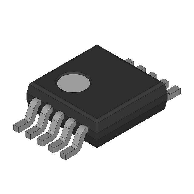
■ 10-pin MSOP package
location.
■ Operating temperature of -40˚C to + 85˚C
The CAT5132 comes with 2 voltage supply inputs: VCC,
the digital supply voltage input and V+, an analog supply
voltage input. These inputs allow the V+ to be as much
APPLICATIONS
as 10 volts higher than the VCC and allow the DPP
■ LCD screen adjustment
terminal values to be as much as 15 volts above ground.
■ Volume control
The CAT5132 can be used as a potentiometer or as a
■ Mechanical potentiometer replacement
two-terminal variable resistor. It is intended for circuit
level adjustments. It is supplied standard in the -40°C to
■ Gain adjustment
+85°C industrial operating temperature range and offered
■ Line impedance matching
in the 10-pin MSOP package.
■ VCOM setting adjustments
■ 128 Resistor taps
BLOCK DIAGRAM
VCC
V+
SDA
127
SCL
RH
A1
128 TAP POSITION
DECODE CONTROL
7-BIT
NONVOLATILE
MEMORY
REGISTER
(DR)
7-BIT WIPER
CONTROL
REGISTER
(WCR)
0
ELEMENTS
A0
127 RESISTIVE
CONTROL LOGIC AND
ADDRESS DECODE
RL
RW
© 2005 by Catalyst Semiconductor, Inc.
Characteristics subject to change without notice
1
Doc. No. 25092, Rev. 01
�CAT5132
PIN CONFIGURATION
SDA
GND
VCC
A1
A0
1
2
3
4
5
10
9
8
7
6
SCL
V+
RL
RW
RH
MSOP 10-Pin Package
PIN DESCRIPTION
Pin
Number
Name
1
SDA
Serial Data Input/Output - Bidirectional Serial Data pin
used to transfer data into and out of the CAT5132. This
is an Open-Drain I/O and can be wire OR'd with other
Open-Drain (or Open Collector) I/Os.
2
GND
Ground
Description
3
VCC
Digital Supply Voltage (2.7V to 5.5V)
4
A1
Address Select Input to select slave address for
2-wire bus.
5
A0
Address Select Input to select slave address for
2-wire bus.
6
RH
High Reference Terminal for the potentiometer
7
RW
Wiper Terminal for the potentiometer
8
RL
Low Reference Terminal for the potentiometer
9
V+
Analog Supply Voltage for the potentiometer (+8.0V to
15.0V)
10
SCL
Serial Bus Clock input for the 2-wire Serial Bus. This
clock is used to clock all data transfers into and out of
the CAT5132
ORDERING INFORMATION
Prefix
Device #
5132
CAT
Company ID
Product
Number
Suffix
R
I
-10
Temperature Range
I = Industrial (-40°C to 85°C)
TE13
Tape & Reel
2500 units/Reel
Resistance
-10: 10k ohms
-50: 50k ohms
-100: 100k ohms
Package
R: MSOP
Z: MSOP (Green with Sn Lead Finish)
ZG: MSOP (Green with NiPd Au Lead Finsh)
Notes:
1. The device used in the above example is a CAT5132R-10TE13 (MSOP, 10k ohms, Tape & Reel).
2. The Industrial Temperature range of -40˚C to +85˚C is standard on the above product.
Doc. No. 25092, Rev. 01
2
© 2005 by Catalyst Semiconductor, Inc.
Characteristics subject to change without notice
�CAT5132
ABSOLUTE MAXIMUM RATINGS
RECOMMENDED OPERATING CONDITIONS
Temperature Under Bias....................-55˚C to +125˚C
VCC = +2.7V to +5.5V
V+ = 8.0V to +15V
Operating Temperature Range: -40˚C to +85˚C
Storage Temperature ........................ -65˚C to +150˚C
Voltage on any SDA, SCL, A0 & A1 pins with respect
to Ground (1)(2) .............................. -2.0V to VCC + 2.0V
COMMENT
Voltage on RH, RL & RW Pins with respect
to Ground .................................... -2.0V to “V+” + 1.0V
Stresses above those listed under “Absolute Maximum Ratings” may cause
permanent damage to the device. These are stress ratings only, and functional
operation of the device at these or any other conditions outside of those listed
in the operational sections of this specification is not implied. Exposure to any
absolute maximum rating for extended periods may affect device performance
and reliability.
VCC with respect to Ground ................... -2.0V to 7.0V
V+ with respect to Ground ................... -2.0V to 16.0V
Wiper Current (10 sec) ...................................... +6mA
Lead Soldering temperature (10 sec) .............. +300˚C
POTENTIOMETER CHARACTERISTICS
(Over recommended operating conditions unless otherwise stated.)
Symbol
Parameter
Limits
Test Conditions
Min
Typ
Max
Units
RPOT
Potentiometer Resistance (100kΩ)
100
kΩ
RPOT
Potentiometer Resistance (50kΩ)
50
kΩ
RPOT
Potentiometer Resistance (10kΩ)
10
kΩ
RTOL
Potentiometer Resistance Tolerance
Power Rating
IW
RW
25• C
Wiper Current
IW = +1mA @ V+ = 12V
Wiper Resistance
IW = +1mA @ V+ = 8V
VTERM
Voltage on RW, RH or RL
RES
Resolution
GND = 0V; V+ = 8V to 15V
+20
%
50
mW
+3
70
150
mA
Ω
110
200
Ω
V+
V
GND
0.78
ALIN
Absolute Linearity
RLIN
Relative Linearity
(2)
(3)
RW(n)(actual) - RW(n)(expected)
(5)
RW(n+1) - [RW(n)+LSB](5)
%
+1
LSB
(4)
+0.5
LSB
(4)
TCRPOT
Temperature Coefficient of RPOT
(1)
TCRatio
Ratiometric Temperature Coefficient
(1)
Potentiometer Capacitances
(1)
10/10/25
pF
RPOT = 50kΩ
0.4
MHz
CH/CL/CW
fc
Frequency Response
+300
ppm/• C
30
ppm/• C
Notes:
1. This parameter is tested initially and after a design or process change that affects the parameter.
2. Absolute linearity is utilized to determine actual wiper voltage versus expected voltage as determined by wiper position when used as a
potentiometer.
3. Relative linearity is utilized to determine the actual change in voltage between two successive tap positions when used as a potentiometer.
4. LSB = (RHM - RLM)/127; where RHM and RLM are the highest and lowest measured values on the wiper terminal.
5. n = 1, 2, ..., 127
© 2005 by Catalyst Semiconductor, Inc.
Characteristics subject to change without notice
3
Doc No. 25092, Rev. 01
�CAT5132
D.C. ELECTRICAL CHARACTERISTICS
(Over recommended operating conditions unless otherwise stated.)
Symbol
Parameter
Test Conditions
Min
Max
Units
ICC1
Power Supply Current
(Volatile Write/Read)
FSCL = 400kHz, SDA Open,
VCC = 5.5V, Input = GND
1
mA
ICC2
Power Supply Current
(Nonvolatile WRITE)
FSCL = 400kHz, SDA Open,
VCC = 5.5V, Input = GND
3.0
mA
ISB(VCC)
Standby Current (VCC = 5V)
VIN = GND or VCC , SDA = VCC
5
µA
ISB(V+)
V+ Standby Current
VCC = 5V, V+ = 15V
10
µA
ILI
Input Leakage Current
VIN = GND to VCC
10
µA
ILO
Output Leakage Current
VOUT = GND to VCC
10
µA
VIL
Input Low Voltage
-1
VCC x 0.3
V
VIH
Input High Voltage
VCC x 0.7
VCC + 1.0
V
VOL1
Output Low Voltage (VCC = 3.0)
0.4
V
Max
Units
IOL = 3mA
CAPACITANCE
TA = 25˚C, f = 1.0MHz, VCC = 5.0V
Symbol
Parameter
Test Conditions
Min
CI/O
Input/Output Capacitance (SDA)
VI/O = 0V (1)
8
pF
CIN
Input Capacitance (A0, A1, SCL)
VIN = 0V (1)
6
pF
A.C. CHARACTERISTICS
VCC = 2.7 - 5.5V
Symbol
Min
Parameter (see Fig. 1)
Max
Units
FSCL
Clock Frequency
400
kHz
TI (1)
Noise Suppression Time Constant at SCL & SDA Inputs
50
ns
tAA
SLC Low to SDA Data Out and ACK Out
1
µs
tBUF
(1)
Time the bus must be free before a new transmission can start
1.2
µs
Start Condition Hold Time
0.6
µs
tLOW
Clock Low Period
1.2
µs
tHIGH
Clock High Period
0.6
µs
tSU:STA
Start Condition Setup Time (for a Repeated Start Condition)
0.6
µs
tHD:DAT
Data in Hold Time
0
ns
tHD:STA
tR
(1)
SDA and SCL Rise Time
0.3
µs
tF
(1)
SDA and SCL Fall Time
300
ns
tSU:STO
tDH
Stop Conditions Setup Time
0.6
µs
Data Out Hold Time
100
ns
Notes:
1. This parameter is tested initially and after a design or process change that affects the parameter.
Doc. No. 25092, Rev. 01
4
© 2005 by Catalyst Semiconductor, Inc.
Characteristics subject to change without notice
�CAT5132
POWER UP TIMING (1)(2)
Symbol
Parameter
Min
Max
Units
tPUR
Power-up to Read Operation
1
ms
tPUW
Power-up to Write Operation
1
ms
XDCP TIMING
Symbol
Parameter
Min
Max
Units
tWRPO
Wiper Response Time After Power Supply Stable
5
10
µs
tWRL
Wiper Response Time After Instruction Issued
5
10
µs
Min
Max
Units
5
ms
WRITE CYCLE LIMITS
Symbol
Parameter
Write Cycle Time (see Fig. 2)
tWR
The write cycle is the time from a valid stop condition of a write sequence to the end of the internal program/erase cycle.
During the write cycle, the bus interface circuits are disabled, SDA is allowed to remain high and the device does not
respond to its slave address.
RELIABILITY CHARACTERISTICS
Symbol
Parameter
Reference Test Method
Min
Max
Units
NEND (1)
Endurance
MIL-STD-883, Test Method 1033
100,000
Cycles/Byte
TDR (1)
Data Retention
MIL-STD-883, Test Method 1008
100
Years
VZAP (1)
ESD Susceptibility
MIL-STD-883, Test Method 3015
2000
Volts
JEDEC Standard 17
100
mA
ILTH
(1)
Latch-Up
Notes:
1. This parameter is tested initially and after a design or process change that affects the parameter.
2. tPUR and tPUW are the delays required from the time VCC is stable until the specified operation can be initiated.
TYPICAL PERFORMANCE CHARACTERISTICS
Resistance between RW and RL
12.000
400
Vcc=2.7V; V+=8v
Vcc=5.5V; V+=15V
10.000
350
300
8.000
Icc2 (uA)
RWL (Kohm)
Icc2 (NV write) vs Temperature
6.000
4.000
250
200
150
Vcc = 2.7V
100
2.000
Vcc = 5.5V
50
0
0.000
0
16
32
48
64
80
96
112
-50
128
-10
10
30
50
70
90
110 130
Temperature (°C)
Tap position
© 2005 by Catalyst Semiconductor, Inc.
Characteristics subject to change without notice
-30
5
Doc No. 25092, Rev. 01
�CAT5132
TYPICAL PERFORMANCE CHARACTERISTICS (CONT)
Relative Linearity Error
Absolute Linearity Error per Tap Position
1.000
Tamb = 25 C
Rtotal = 10K
0.800
0.300
RLIN Error (LSB)
0.400
0.200
0.000
-0.200
-0.400
0.100
0.000
-0.100
-0.200
-0.300
-0.800
-0.400
0
16
32
48
64
80
96
112
Vcc=5.5V; V+=15V
0.200
-0.600
-1.000
Vcc=2.7V; V+=8V
Tamb = 25 C
Rtotal = 10K
0.400
Vcc=5.5V; V+=15V
0.600
ALIN Error (LSB)
0.500
Vcc=2.7V; V+=8v
-0.500
128
0
16
Tap position
32
48
64
80
96
112
128
Tap position
tF
tHIGH
tLOW
tR
tLOW
SCL
tSU:STA
tHD:DAT
tHD:STA
tSU:DAT
tSU:STO
SDA IN
tAA
tBUF
tDH
SDA OUT
Figure 1. Bus Timing
SCL
SDA
8TH BIT
ACK
BYTE n
tWR
STOP
CONDITION
START
CONDITION
ADDRESS
Figure 2. Write Cycle Timing
Doc. No. 25092, Rev. 01
6
© 2005 by Catalyst Semiconductor, Inc.
Characteristics subject to change without notice
�CAT5132
Acknowledge
SERIAL BUS PROTOCOL
After a successful data transfer, each receiving device
is required to generate an acknowledge. The
Acknowledging device pulls down the SDA line during
the ninth clock cycle, signaling that it received the 8 bits
of data (see Fig. 4).
The following defines the features of the 2-wire bus
protocol:
(1) Data transfer may be initiated only when the bus is
not busy.
(2) During a data transfer, the data line must remain
stable whenever the clock line is high. Any changes
in the data line while the clock is high will be
interpreted as a START or STOP condition.
The CAT5132 responds with an acknowledge after
receiving a START condition and its slave address. If
the device has been selected along with a write operation,
it responds with an acknowledge after receiving each
8-bit byte.
The device controlling the transfer is a master, typically
a processor or controller, and the device being controlled
is the slave. The master will always initiate data transfers
and provide the clock for both transmit and receive
operations. Therefore, the CAT5132 will be considered
a slave device in all applications.
When the CAT5132 is in a READ mode it transmits 8 bits
of data, releases the SDA line, and monitors the line for
an acknowledge. Once it receives this acknowledge,
the CAT5132 will continue to transmit data. If no
acknowledge is sent by the Master, the device terminates
data transmission and waits for a STOP condition.
START Condition
Acknowledge Polling
The START Condition precedes all commands to the
device, and is defined as a HIGH to LOW transition of
SDA when SCL is HIGH. The CAT5132 monitors the
SDA and SCL lines and will not respond until this
condition is met (see Fig. 3).
The disabling of the inputs can be used to take advantage
of the typical write cycle time. Once the stop condition is
issued to indicate the end of the host's write operation,
the CAT5132 initiates the internal write cycle. ACK
polling can be initiated immediately. This involves issuing
the start condition followed by the slave address. If the
CAT5132 is still busy with the write operation, no ACK
will be returned. If the CAT5132 has completed the write
operation, an ACK will be returned and the host can then
proceed with the next instruction operation.
STOP Condition
A LOW to HIGH transition of SDA when SCL is HIGH
determines the STOP condition. All operations must end
with a STOP condition (see Fig. 3).
SDA
SCL
START CONDITION
STOP CONDITION
Figure 3. Start/Stop Condition
SCL FROM
MASTER
1
8
9
DATA OUTPUT
FROM TRANSMITTER
DATA OUTPUT
FROM RECEIVER
ACKNOWLEDGE
START
Figure 4. Acknowledge Condition
© 2005 by Catalyst Semiconductor, Inc.
Characteristics subject to change without notice
7
Doc No. 25092, Rev. 01
�CAT5132
The next two bits, A1 and A0, are the internal slave
address and must match the physical device address
which is defined by the state of the A1 and A0 input pins
to successfully address the CAT5132. Only the device
with slave address matching the input byte will be
accessed by the master. This allows up to 4 devices to
reside on the same bus. The A1 and A0 inputs can be
actively driven by CMOS input signals or tied to VCC or
Ground.
DEVICE DESCRIPTION
Access Control Register
The volatile register WCR and the non-volatile register
DR of CAT5132 are accessed only by addressing the
volatile Access Register AR first, using the 3 byte I2C
interface for all read and write operations (see Table 1).
The first byte is the slave address/instruction byte (see
details below). The second byte contains the address
(02h) of the AR register. The data in the third byte
controls which register WCR (80h) or DR (00h) is being
addressed (see Figure 5).
The last bit is the READ/WRITE bit and determines the
function to be performed. If it is a “1” a read command is
initiated and if it is a “0” a write is initiated. For the AR
register only write is allowed.
Slave Address Instruction Byte Description
The first byte sent to the CAT5132 from the master
processor is called the Slave/DPP Address Byte. The
most significant five bits of the slave address are a
device type identifier. These bits for the CAT5132 are
fixed at 01010 (refer to Table 2).
After the Master sends a START condition and the slave
address byte, the CAT5132 monitors the bus and
responds with an acknowledge (on the SDA line) when
its address matches the transmitted slave address.
Table 1. Access Control Register
ID2
ID1
ID0
A1
A0
Wb
ACK
ACK
STOP
ST
0
1
0
1
0
0
0
0
A
0
0
0
0
0
0
1
0
A
1
0
0
0
0
0
0
0
A
SP
ST
0
1
0
1
0
0
0
0
A
0
0
0
0
0
0
1
0
A
0
0
0
0
0
0
0
0
A
SP
ACK
ID3
3rd byte
ID4
2nd byte
START
1st byte
A R address - 02h
WCR(80h) / DR (00h) selection
Table 2. Byte 1 Slave Address and Instruction Byte
Device Type Identifier
Read/Write
Slave Address
ID4
ID3
ID2
ID1
ID0
A1
A0
R/W
0
1
0
1
0
X
X
X
(MSB)
(LSB)
BUS ACTIVITY:
MASTER
SDA LINE
SLAVE
ADDRESS
S
T & INSTRUCTION
A
R
FIXED
T
AR REGISTER
ADDRESS
WCR/DR
SELECTION
S
T
O
P
P
S
VARIABLE
A
C
K
A
C
K
A
C
K
Figure 5. Access Register Addressing Using 3 Bytes
Doc. No. 25092, Rev. 01
8
© 2005 by Catalyst Semiconductor, Inc.
Characteristics subject to change without notice
�CAT5132
Wiper Control Register (WCR) Description
The CAT5132 contains a 7-bit Wiper Control Register
which is decoded to select one of the 128 switches along
its resistor array. The WCR is a volatile register and is
written with the contents of the nonvolatile Data Register
(DR) on power-up. The Wiper Control Register loses its
contents when the CAT5132 is powered-down. The
contents of the WCR may be read or changed directly by
the host using a READ/WRITE command after addressing
the WCR (see Table 1 to access WCR). Since the
CAT5132 will only make use of the 7 LSB bits (The first
data bit, or MSB, is ignored) on write instructions and will
always come back as a “0” on read commands.
A write operation (see Table 3) requires a Start condition, followed by a valid slave address byte, a valid address byte
00h, a data byte and a STOP condition. After each of the three bytes the CAT5132 responds with an acknowledge.
At this time the data is written only to volatile registers, then the device enters its standby state.
Table 3. WCR Write Operation
0
ST
slave address byte
0
1
0
1
0
0
A
AR address - 02h
0
0
0
0
A
0
0
0
0
1
0
WCR address - 00h
0
0
0
0
0
0
A
WCR(80h) selection
1
0
0
0
0
A
0
0
0
0
0
X
X
X
data byte
X
X
X
X
X
STOP
Wb
0
A
SP
STOP
A0
0
ACK
A1
0
ACK
ID0
1
ACK
ID1
0
3rd byte
ACK
ID2
1
ACK
ID3
0
2nd byte
ACK
ID4
ST
START
START
1st byte
A
SP
An increment operation (see Table 4) requires a Start condition, followed by a valid increment address byte (01011),
a valid address byte 00h. After each of the two bytes, the CAT5132 responds with an acknowledge. At this time if the
data is high then the wiper is incremented or if the data is low the wiper is decremented at each clock. Once the stop
is issued then the device enters its standby state with the WCR data as being the last inc/dec position. Also, the wiper
position does not roll over but is limited to min and max positions.
Table 4. WCR Increment/Decrement Operation
Wb
0
0
ST
slave address byte
0
1
0
1
1
0
A
AR address - 02h
0
0
0
0
A
0
0
0
0
1
0
WCR address - 00h
0
0
0
0
0
0
A
WCR(80h) selection
1
0
0
A
0
0
0
0
0
0
0
STOP
A0
0
A
SP
STOP
A1
0
ACK
ID0
1
ACK
ID1
0
3rd byte
ACK
ID2
1
ACK
ID3
0
2nd byte
ACK
ID4
ST
START
START
1st byte
increment (1) / decrement (0) bits
1
1
1
1
0
0
0
SP
0
A read operation (see Table 5) requires a Start condition, followed by a valid slave address byte for write, a valid address
byte 00h, a second START and a second slave address byte for read. After each of the three bytes, the CAT5132
responds with an acknowledge and then the device transmits the data byte. The master terminates the read operation
by issuing a STOP condition following the last bit of Data byte.
Table 5. WCR Read Operation
A0
Wb
0
0
0
slave address byte
0
1
START
ST
ST
0
1
0
0
A
0
0
0
0
A
0
1
0
1
0
0
0
0
1
0
0
0
0
0
0
0
0
0
X
X
X
data byte
0
© 2005 by Catalyst Semiconductor, Inc.
Characteristics subject to change without notice
1
A
A
1
0
0
0
0
0
0
0
A
SP
WCR address - 00h
slave address byte
0
0
STOP
A1
0
ACK
ID0
1
ACK
ID1
0
3rd byte
WCR(80h) selection
STOP
ID2
1
ACK
ID3
0
2nd byte
AR address - 02h
ACK
ID4
ST
START
START
1st byte
0
X
X
X
X
9
SP
Doc No. 25092, Rev. 01
�CAT5132
Data Register (DR)
being performed. During the internal non-volatile write
cycle, the device ignores transitions at the SDA and SCL
pins, and the SDA output is at a high impedance state.
The WCR is also written during a write to DR. After a DR
WRITE is complete the DR and WCR will contain the
same wiper position.
The Data Register (DR) is a nonvolatile register and its
contents are automatically written to the Wiper Control
Register (WCR) on power-up. It can be read at any time
without effecting the value of the WCR. The DR, like the
WCR, only stores the 7 LSB bits and will report the MSB
bit as a “0”. Writing to the DR is performed in the same
fashion as the WCR except that a time delay of up to 5ms
is experienced while the nonvolatile store operation is
To write or read to the DR, first the access to DR is selected, see table 1 then the data is written or read using the
following sequences.
A write operation (see Table 6) requires a Start condition, followed by a valid slave address byte, a valid address byte
00h, a data byte and a STOP condition. After each of the three bytes the CAT5132 responds with an acknowledge.
At this time the data is written both to volatile and non-volatile registers, then the device enters its standby state.
A0
Wb
0
0
0
slave address byte
0
1
0
1
0
0
0
0
ACK
START
ST
A
0
0
A
0
0
0
0
1
0
DR address - 00h
0
0
0
0
0
0
A
DR(00h) selection
0
0
0
0
0
A
0
0
0
0
0
X
X
X
data byte
X
X
X
X
X
STOP
A1
0
A
SP
STOP
ID0
1
ACK
ID1
0
ACK
ID2
1
3rd byte
ACK
ID3
0
2nd byte
AR address - 02h
ACK
ID4
ST
1st byte
ACK
START
Table 6. DR Write Operation
A
SP
A read operation (see Table 7) requires a Start condition, followed by a valid slave address byte, a valid address byte
00h, a second Start and a second slave address byte for read. After each of the three bytes the CAT5132 responds
with an acknowledge and then the device transmits the data byte. The master terminates the read operation by issuing
a STOP condition following the last bit of Data byte.
ID0
A1
A0
Wb
1
0
0
0
0
0
1
ST
0
1
0
0
0
0
ACK
START
slave address byte
START
ST
A
0
0
A
0
1
0
Doc. No. 25092, Rev. 01
1
0
0
0
0
1
0
0
0
0
0
0
0
0
0
X
X
X
data byte
0
1
A
A
0
0
0
0
0
0
0
0
A
SP
DR address - 00h
slave address byte
0
0
DR(00h) selection
STOP
ID1
0
AR address - 02h
ACK
ID2
1
3rd byte
ACK
ID3
0
2nd byte
STOP
ID4
ST
1st byte
ACK
START
Table 7. DR Read Operation
0
X
X
X
X
10
SP
© 2005 by Catalyst Semiconductor, Inc.
Characteristics subject to change without notice
�CAT5132
POTENTIOMETER OPERATION
Power-On
This offset will appear in each of the CAT5132 end-toend resistance values in the same way as the 10kΩ
example. However resistance between each wiper
position for the 50kΩ version will be ~395Ω and for the
100kΩ version will be ~790Ω.
The CAT5132 is a 128-position, digital controlled
potentiometer. At power-up the device turns on at the
mid-point wiper location (64) until the wiper register can
be loaded with the nonvolatile memory location previously
stored in the device. After the nonvolatile memory data
is loaded into the wiper register the wiper location will
change to the previously stored wiper position.
Table 8. Potentiometer Resistance and Wiper
Resistance Offset Effects
The end-to-end nominal resistance of the potentiometer
has 128 contact points linearly distributed across the
total resistor. Each of these contact points is addressed
by the 7 bit wiper register which is decoded to select one
of these 128 contact points.
Position
Each contact point generates a linear resistive value
between the 0 position and the 127 position. These
values can be determined by dividing the end-to-end
value of the potentiometer by 127. In the case of the
10kΩ potentiometer~79Ω is the resistance between
each wiper position. However in addition to the ~79Ω for
each resistive segment of the potentiometer, a wiper
resistance offset must be considered. Table 8 shows the
effect of this value and how it would appear on the wiper
terminal.
© 2005 by Catalyst Semiconductor, Inc.
Characteristics subject to change without notice
00
70Ω or
0Ω + 70Ω
01
149Ω or
79Ω + 70Ω
63
5,047Ω or
4,977Ω + 70Ω
127
10,070Ω or
10,000Ω + 70Ω
Position
11
Typical RW to RL Resistance for
10kΩ DPP
Typical RW to RH Resistance for
10kΩ DPP
00
10,070Ω or
10,000Ω + 70Ω
64
5,047Ω or
4,977Ω + 70Ω
126
149Ω or
79Ω + 70Ω
127
70Ω or
0Ω + 70Ω
Doc No. 25092, Rev. 01
�CAT5132
PACKAGE OUTLINES
10-LEAD MSOP
Doc. No. 25092, Rev. 01
12
© 2005 by Catalyst Semiconductor, Inc.
Characteristics subject to change without notice
�REVISION HISTORY
Date
Rev.
Reason
09/12/2005
00
Initial Issue
01/18/2006
01
Update Ordering Information
Copyrights, Trademarks and Patents
Trademarks and registered trademarks of Catalyst Semiconductor include each of the following:
DPP ™
AE2 ™
MiniPot™
Catalyst Semiconductor has been issued U.S. and foreign patents and has patent applications pending that protect its products. For a complete list of patents
issued to Catalyst Semiconductor contact the Company’s corporate office at 408.542.1000.
CATALYST SEMICONDUCTOR MAKES NO WARRANTY, REPRESENTATION OR GUARANTEE, EXPRESS OR IMPLIED, REGARDING THE SUITABILITY OF ITS
PRODUCTS FOR ANY PARTICULAR PURPOSE, NOR THAT THE USE OF ITS PRODUCTS WILL NOT INFRINGE ITS INTELLECTUAL PROPERTY RIGHTS OR THE
RIGHTS OF THIRD PARTIES WITH RESPECT TO ANY PARTICULAR USE OR APPLICATION AND SPECIFICALLY DISCLAIMS ANY AND ALL LIABILITY ARISING
OUT OF ANY SUCH USE OR APPLICATION, INCLUDING BUT NOT LIMITED TO, CONSEQUENTIAL OR INCIDENTAL DAMAGES.
Catalyst Semiconductor products are not designed, intended, or authorized for use as components in systems intended for surgical implant into the body, or
other applications intended to support or sustain life, or for any other application in which the failure of the Catalyst Semiconductor product could create a
situation where personal injury or death may occur.
Catalyst Semiconductor reserves the right to make changes to or discontinue any product or service described herein without notice. Products with data sheets
labeled "Advance Information" or "Preliminary" and other products described herein may not be in production or offered for sale.
Catalyst Semiconductor advises customers to obtain the current version of the relevant product information before placing orders. Circuit diagrams illustrate
typical semiconductor applications and may not be complete.
Catalyst Semiconductor, Inc.
Corporate Headquarters
1250 Borregas Avenue
Sunnyvale, CA 94089
Phone: 408.542.1000
Fax: 408.542.1200
www.catalyst-semiconductor.com
Publication #:
Revison:
Issue date:
25092
01
01/18/06
�