CAT811
Voltage Supervisor, 4-Pin,
Push-Pull, Active Low, with
Manual Reset
Description
The CAT811 is a microprocessor supervisory circuit that monitors
power supplies. The CAT811 is a direct replacement for the MAX811
in applications operating over the industrial temperature range and has
a manual reset input.
These devices generate a reset signal, which is asserted while the
power supply voltage is below a preset threshold level and for at least
140 ms after the power supply level has risen above that level. The
underlying floating gate technology, Analog EEPROM used by ON
Semiconductor, makes it possible to offer any custom reset threshold
value. Seven industry standard threshold levels are offered to support
+5.0 V, +3.3 V, +3.0 V and +2.5 V systems. The CAT811 features a
RESET push−pull output (active LOW).
Fast transients on the power supply are ignored and the output is
guaranteed to be in the correct state at Vcc levels as low as 1.0 V.
The CAT811 is fully specified over the industrial temperature range
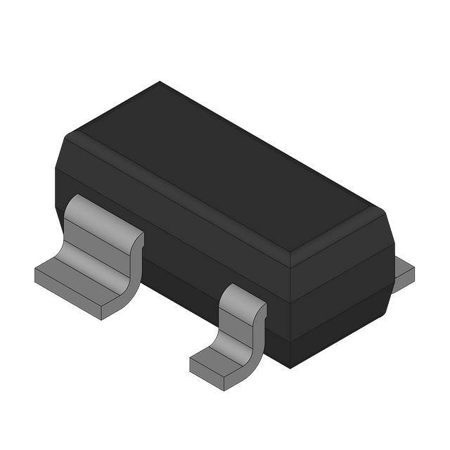
(−40°C to 85°C) and is available in a compact 4−pin SOT−143
package.
www.onsemi.com
SOT−143
BI SUFFIX
CASE 527AF
PIN CONFIGURATION
1
2
• Precision Monitoring of
•
•
•
•
•
•
+5.0 V (± 5%, ± 10%, ± 20%),
+3.3 V (± 5%, ± 10%)
Manual Reset Input
Output Configuration: Active LOW Reset
Direct Replacements for the MAX811 in Applications Operating
over the Industrial Temperature Range
Reset Valid down to VCC = 1.0 V
6 mA Power Supply Current
Power Supply Transient Immunity
Available in SOT−143 Packages with Sn or NiPdAu Green Lead
Finishes
Industrial Temperature Range: −40°C to +85°C
These Devices are Pb−Free, Halogen Free/BFR Free and are RoHS
Compliant
July, 2015 − Rev. 3
MR
(Top View)
MARKING DIAGRAM
XXXMG
G
1
XXX
M
G
= Specific Device Code
= Month Code
= Pb−Free Package
(Note: Microdot may be in either location)
ORDERING INFORMATION
See detailed ordering and shipping information in the package
dimensions section on page 9 of this data sheet.
Computers, Servers, Laptops and Cable Modems
Wireless Communications
Embedded Control Systems
White Goods, Power Meters
Intelligent Instruments
PDAs and Handheld Equipment
© Semiconductor Components Industries, LLC, 2015
3
RESET
Applications
•
•
•
•
•
•
VCC
GND
Features
•
•
•
4
1
Publication Order Number:
CAT811/D
�CAT811
Table 1. THRESHOLD SUFFIX SELECTOR DESCRIPTION
Nominal Threshold Voltage
Threshold Suffix Designation
4.63 V
L
3.08 V
T
2.93 V
S
Table 2. PIN DESCRIPTION
Pin Number
Pin Name
Description
1
GND
2
RESET
3
MR
Manual Reset Input. A logic LOW on MR asserts RESET. RESET remains active as long as MR is
LOW and for 140 ms after MR returns HIGH. The active low input has an internal 20 kW pull−up resistor. The input should be left open if not used.
4
VCC
Power supply voltage that is monitored.
Ground.
Active LOW reset. RESET is asserted if VCC falls below the reset threshold and remains low for at
least 140 ms after VCC rises above the reset threshold.
VCC
MR
VCC
VCC
TOLERANCE
BIAS
RESET
&
DIGITAL
DELAY
+
–
RESET
VOLTAGE
REFERENCE
CAT811
GND
Figure 1. Block Diagrams
www.onsemi.com
2
�CAT811
Table 3. ABSOLUTE MAXIMUM RATINGS
Parameters
Ratings
Units
−0.3 to +6.0
V
Input Current, VCC
20
mA
Output Current RESET
20
mA
Rate of Raise, VCC
100
V/ms
Continuous Power Dissipations
Derate 4 mW/°C above +70°C (SOT−143)
320
mW
Storage Temperature Range
−65 to +105
°C
Operating Ambient Temperature Range
−40 to +85
°C
+300
°C
Any pin with respect to ground
Lead Soldering Temperature (10 seconds)
Stresses exceeding those listed in the Maximum Ratings table may damage the device. If any of these limits are exceeded, device functionality
should not be assumed, damage may occur and reliability may be affected.
Table 4. ELECTRICAL OPERATING CHARACTERISTICS
(VCC = Full range, TA = −40°C to +85°C unless otherwise noted. Typical values at TA = +25°C and VCC = 5 V for the L version,
VCC = 3.3 V for the T/S versions.)
Parameter
Symbol
VCC Range
Supply Current
Reset Threshold
Voltage
ICC
VTH
Conditions
Min
TA = 0°C to +70°C
TA = −40°C to +85°C
TA = −40°C to +85°C
Typ
Max
Units
1.0
5.5
V
1.2
5.5
VCC < 5.5 V, L
8
20
VCC < 3.6 V, S/T
6
15
4.63
4.70
L Threshold
TA = +25°C
4.56
TA = −40°C to +85°C
4.50
TA = +25°C
3.04
TA = −40°C to +85°C
3.00
TA = +25°C
2.89
TA = −40°C to +85°C
2.85
T Threshold
S Threshold
Reset Threshold
Tempco
VCC to Reset Delay
(Note 3)
VCC = VTH to (VTH − 100 mV)
Reset Active
Timeout Period
TA = −40°C to +85°C
1. Production testing done at TA = +25°C; limits over temperature guaranteed by design only.
2. Glitches of 100 ns or less typically will not generate a reset pulse.
3. RESET output for the CAT811.
www.onsemi.com
3
140
mA
V
4.75
3.08
3.11
3.15
2.93
2.96
3.00
30
ppm/°C
20
ms
240
400
ms
�CAT811
Table 4. ELECTRICAL OPERATING CHARACTERISTICS
(VCC = Full range, TA = −40°C to +85°C unless otherwise noted. Typical values at TA = +25°C and VCC = 5 V for the L version,
VCC = 3.3 V for the T/S versions.)
Parameter
Symbol
Conditions
RESET Output
Voltage Low
(Push−pull, active
LOW, CAT811)
VOL
RESET Output
Voltage High
(Push−pull, active
LOW, CAT811)
VOH
MR Minimum Pulse
Width
tMR
MR Glitch Immunity
Min
Typ
Max
Units
VCC = VTH min, ISINK = 1.2 mA CAT811S/T
0.3
V
VCC = VTH min, ISINK = 3.2 mA CAT811L
0.4
VCC > 1.0 V, ISINK = 50 mA
0.3
VCC = VTH max, ISOURCE = 500 mA CAT811S/T
0.8VCC
V
VCC = VTH max, ISOURCE = 800 mA CAT811L
VCC − 1.5
V
10
ms
(Note 2)
100
ns
0.5
ms
MR to RESET
Propagation Delay
tMD
(Note 3)
MR Input Threshold
VIH
VCC > VTH (MAX), CAT811L
V
2.3V
VIL
VIH
0.8
VCC > VIH (MAX), CAT811S/T
0.7VCC
VIL
0.25VCC
MR Pull−up
Resistance
10
1. Production testing done at TA = +25°C; limits over temperature guaranteed by design only.
2. Glitches of 100 ns or less typically will not generate a reset pulse.
3. RESET output for the CAT811.
www.onsemi.com
4
20
75
kW
�CAT811
TYPICAL OPERATING CHARACTERISTICS
(VCC = Full range, TA = −40°C to +85°C unless otherwise noted. Typical values at TA = +25°C and VCC = 5 V for the L version,
VCC = 3.3 V for the T/S versions.)
SUPPLY CURRENT (mA)
240
VCC = 5 V
220
VCC = 2.5 V
200
180
160
−50
POWER−DOWN RESET DELAY (s)
12
0
50
100
10
VCC = 5.5 V
8
4
2
0
50
100
150
TEMPERATURE (°C)
TEMPERATURE (°C)
Figure 2. Power−Up Reset Timeout vs.
Temperature
Figure 3. Supply Current vs. Temperature
(No Load, CAT811S/T)
14
1.0002
12
1.0000
10
8
6
4
2
0
−50
VCC = 3.6 V
6
0
−50
150
NORMALIZED THRESHOLD
POWER−UP RESET TIMEOUT (ms)
260
0.9998
0.9996
0.9994
0.9992
0.9990
0.9988
0
50
100
0
150
20
40
60
80
100
TEMPERATURE (°C)
TEMPERATURE (°C)
Figure 4. Power−Down Reset Delay vs.
Temperature (CAT811S/T)
Figure 5. Normalized Reset Threshold vs.
Temperature
www.onsemi.com
5
120
�CAT811
DETAILED DESCRIPTION
Reset Timing
The reset signal is asserted LOW for the CAT811 when the power supply voltage falls below the threshold trip voltage and
remains asserted for at least 140 ms after the power supply voltage has risen above the threshold.
Threshold
Voltage
5V
VCC
0V
140 ms
minimum
5V
CAT811
RESET
Reset
Timeout Period
0V
VCC
CAT812
RESET
0V
Figure 6. Reset Timing Diagram
VCC Transient Response
Valid Reset with VCC under 1.0 V
The CAT811 protect mPs against brownout failure. Short
duration transients of 4 ms or less and 100 mV amplitude
typically do not cause a false RESET.
Figure 7 shows the maximum pulse duration of
negative−going VCC transients that do not cause a reset
condition. As the amplitude of the transient goes further
below the threshold (increasing VTH − VCC), the maximum
pulse duration decreases. In this test, the VCC starts from an
initial voltage of 0.5 V above the threshold and drops below
it by the amplitude of the overdrive voltage (VTH − VCC).
To ensure that the CAT811 RESET pin is in a known state
when VCC is under 1.0 V, a 100 kW pull−down resistor
between RESET pin and GND is recommended; the value
is not critical.
Power
Supply
VCC
CAT811
30
MR RESET
TRANSIENT DURATION (ms)
TAMB = 25°C
GND
100 kW
25
20
CAT811Z
Figure 8. RESET Valid with VCC Under 1.0 V
15
CAT811M
10
5
0
1
10
100
1000
RESET OVERDRIVE VTH − VCC (mV)
Figure 7. Maximum Transient Duration without
Causing a Reset Pulse vs. Reset Comparator
Overdrive
www.onsemi.com
6
�CAT811
Bi−directional Reset Pin Interfacing
The CAT811 can interface with mP/mC bi−directional reset pins by connecting a 4.7 kW resistor in series with the CAT811
reset output and the mP/mC bi−directional reset pin.
BUF
Buffered
RESET
Power
Supply
CAT811
VCC
mP
4.7 kW
MR
RESET
(for example: 68HC11)
RESET
INPUT
C AT8 11
GND
GND
Bi−directional I/O Pin
Figure 9. Bi−directional Reset Pin Interfacing
Table 5. OTHER SUPERVISORY PRODUCTS
Function
CAT1161/3
CAT1162
With 16k Bit Serial EEPROM Memory
a
a
Watchdog Timer
a
Manual Reset Input
a
CAT809
a
a
a
Active High Reset
Package
CAT811
a
a
Active Low Reset
Dual Polarity Reset Outputs
CAT810
a
a
8−pin DIP
and SOIC
8−pin DIP
and SOIC
www.onsemi.com
7
3−pin SOT−23
and SC70
3−pin SOT−23
and SC70
4−pin
SOT−143
�CAT811
ORDERING INFORMATION
Order Number
Output
Reset
Package
Quantity
per Reel
(Note 5)
Manual
Reset
LOW
SOT−143−4
3,000
Top Mark (Note 4)
NiPdAu
Voltage
NiPdAu
CAT811LTBI−GT3
4.63 V
VEA
CAT811MTBI−GT3
4.38 V
VEA
CAT811JTBI−GT3
4.00 V
VEA
CAT811TTBI−GT3
3.08 V
VEA
CAT811STBI−GT3
2.93 V
VEA
CAT811RTBI−GT3
2.63 V
VEA
CAT811ZTBI−GT3
2.32 V
VEA
4. Threshold and full part numbers will be provided on box and reel labels as well as all Shipping documents.
5. For information on tape and reel specifications, including part orientation and tape sizes, please refer to our Tape and Reel Packaging
Specifications Brochure, BRD8011/D.
6. For detailed information and a breakdown of device nomenclature and numbering systems, please see the ON Semiconductor Device
Nomenclature document, TND310/D, available at www.onsemi.com
www.onsemi.com
8
�MECHANICAL CASE OUTLINE
PACKAGE DIMENSIONS
SOT−143, 4 Lead
CASE 527AF−01
ISSUE A
DATE 24 MAR 2009
SYMBOL
MIN
A
0.80
1.22
D
A1
0.05
0.15
e
A2
0.75
b
0.30
0.50
b2
0.76
0.89
4
3
E1
1
E
c
0.08
D
2.80
E
2.10
E1
1.20
e
2
0.40
L1
2.64
1.30
0.50
0°
1.40
0.60
8°
q
A
3.04
0.25
θ
A2
0.20
2.90
0.54 REF
L2
TOP VIEW
1.07
0.20 BSC
L
b
0.90
MAX
1.92 BSC
e1
e1
NOM
c
L2
L
b2
A1
L1
SIDE VIEW
END VIEW
Notes:
(1) All dimensions are in millimeters. Angles in degrees.
(2) Complies with JEDEC TO-253.
DOCUMENT NUMBER:
DESCRIPTION:
98AON34306E
SOT−143, 4 LEAD
Electronic versions are uncontrolled except when accessed directly from the Document Repository.
Printed versions are uncontrolled except when stamped “CONTROLLED COPY” in red.
PAGE 1 OF 1
ON Semiconductor and
are trademarks of Semiconductor Components Industries, LLC dba ON Semiconductor or its subsidiaries in the United States and/or other countries.
ON Semiconductor reserves the right to make changes without further notice to any products herein. ON Semiconductor makes no warranty, representation or guarantee regarding
the suitability of its products for any particular purpose, nor does ON Semiconductor assume any liability arising out of the application or use of any product or circuit, and specifically
disclaims any and all liability, including without limitation special, consequential or incidental damages. ON Semiconductor does not convey any license under its patent rights nor the
rights of others.
© Semiconductor Components Industries, LLC, 2019
www.onsemi.com
�onsemi,
, and other names, marks, and brands are registered and/or common law trademarks of Semiconductor Components Industries, LLC dba “onsemi” or its affiliates
and/or subsidiaries in the United States and/or other countries. onsemi owns the rights to a number of patents, trademarks, copyrights, trade secrets, and other intellectual property.
A listing of onsemi’s product/patent coverage may be accessed at www.onsemi.com/site/pdf/Patent−Marking.pdf. onsemi reserves the right to make changes at any time to any
products or information herein, without notice. The information herein is provided “as−is” and onsemi makes no warranty, representation or guarantee regarding the accuracy of the
information, product features, availability, functionality, or suitability of its products for any particular purpose, nor does onsemi assume any liability arising out of the application or use
of any product or circuit, and specifically disclaims any and all liability, including without limitation special, consequential or incidental damages. Buyer is responsible for its products
and applications using onsemi products, including compliance with all laws, regulations and safety requirements or standards, regardless of any support or applications information
provided by onsemi. “Typical” parameters which may be provided in onsemi data sheets and/or specifications can and do vary in different applications and actual performance may
vary over time. All operating parameters, including “Typicals” must be validated for each customer application by customer’s technical experts. onsemi does not convey any license
under any of its intellectual property rights nor the rights of others. onsemi products are not designed, intended, or authorized for use as a critical component in life support systems
or any FDA Class 3 medical devices or medical devices with a same or similar classification in a foreign jurisdiction or any devices intended for implantation in the human body. Should
Buyer purchase or use onsemi products for any such unintended or unauthorized application, Buyer shall indemnify and hold onsemi and its officers, employees, subsidiaries, affiliates,
and distributors harmless against all claims, costs, damages, and expenses, and reasonable attorney fees arising out of, directly or indirectly, any claim of personal injury or death
associated with such unintended or unauthorized use, even if such claim alleges that onsemi was negligent regarding the design or manufacture of the part. onsemi is an Equal
Opportunity/Affirmative Action Employer. This literature is subject to all applicable copyright laws and is not for resale in any manner.
PUBLICATION ORDERING INFORMATION
LITERATURE FULFILLMENT:
Email Requests to: orderlit@onsemi.com
onsemi Website: www.onsemi.com
◊
TECHNICAL SUPPORT
North American Technical Support:
Voice Mail: 1 800−282−9855 Toll Free USA/Canada
Phone: 011 421 33 790 2910
Europe, Middle East and Africa Technical Support:
Phone: 00421 33 790 2910
For additional information, please contact your local Sales Representative
�