CAT811, CAT812 4-Pin Microprocessor Power Supply Supervisors with Manual Reset
FEATURES
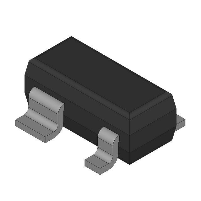
Precision monitoring of +5.0 V (± 5%, ± 10%, ± 20%), +3.3 V (± 5%, ± 10%), +3.0 V (± 10%) and +2.5 V (± 5%) power supplies Manual reset input Offered in two output configurations: CAT811: Active LOW reset CAT812: Active HIGH reset Direct replacements for the MAX811 and MAX812 in applications operating over the industrial temperature range Reset valid down to VCC = 1.0V 6µA power supply current Power supply transient immunity Available in SOT-143 packages with Sn or NiPdAu Green Lead finishes. Industrial temperature range: -40ºC to +85ºC
DESCRIPTION
The CAT811 and CAT812 are microprocessor supervisory circuits that monitor power supplies. The CAT811 and CAT812 are direct replacements for the MAX811 and MAX812 in applications operating over the industrial temperature range; both have a manual reset input. These devices generate a reset signal, which is asserted while the power supply voltage is below a preset threshold level and for at least 140ms after the power supply level has risen above that level. The underlying floating gate technology, AE2(TM) used by Catalyst Semiconductor, makes it possible to offer any custom reset threshold value. Seven industry standard threshold levels are offered to support +5.0V, +3.3V, +3.0V and +2.5V systems. The CAT811 features a RESET push-pull output (active LOW) and the CAT812 features a RESET push-pull output (active HIGH). Fast transients on the power supply are ignored and the output is guaranteed to be in the correct state at Vcc levels as low as 1.0 V. The CAT811/812 are fully specified over the industrial temperature range (-40°C to 85°C) and are available in a compact 4-pin SOT-143 package. For Ordering Information details, see page 10.
APPLICATION
Computers, Servers, Laptops Cable modems Wireless communications Embedded control systems White goods Power meters Intelligent instruments PDAs and handheld equipment
THRESHOLD SUFFIX SELECTOR DESCRIPTION
Nominal Threshold Voltage 4.63V 4.38V 4.00V 3.08V 2.93V 2.63V 2.32V Threshold Suffix Designation L M J T S R Z
PIN CONFIGURATION
GND 1 CAT811 CAT812 ¯¯¯¯¯¯ RESET 2 3 ¯¯¯ MR 4 VCC
© 2010 SCILLC. All rights reserved. Characteristics subject to change without notice
1
Doc. No. MD-3005 Rev. U
�CAT811, CAT812
PIN DESCRIPTION
Pin Number CAT811 CAT812 1 2 — 1 — 2 Name GND ¯¯¯¯¯¯ RESET RESET Description Ground Active LOW reset. ¯¯¯¯¯¯ is asserted if VCC f alls below the reset threshold RESET and remains low for at least 140ms after VCC rises above the reset threshold. Active HIGH reset. RESET is asserted if VCC f alls below the reset threshold and remains high for at least 140ms after VCC rises above the reset threshold. Manual Reset Input. A logic LOW on ¯¯¯ asserts RESET. RESET remains MR active as long as ¯¯¯ is LOW and for 140ms after ¯¯¯ returns HIGH. The MR MR active low input has an internal 20kΩ pull-up resistor. The input should be left open if not used. Power supply voltage that is monitored.
3 4
3 4
¯¯¯ MR VCC
BLOCK DIAGRAM
MR VCC TOLERANCE BIAS RESET & DIGITAL DELAY
VCC
VCC
+ –
RESET
VOLTAGE REFERENCE
CAT811
GND
MR VCC TOLERANCE BIAS RESET & DIGITAL DELAY
VCC
VCC
+ –
RESET
VOLTAGE REFERENCE
CAT812
GND
Doc. No. MD-3005 Rev. U
2
© 2010 SCILLC. All rights reserved. Characteristics subject to change without notice
�CAT811, CAT812
ABSOLUTE MAXIMUM RATINGS (1)
Parameters Any pin with respect to ground Input Current, VCC ¯¯¯¯¯¯ Output Current RESET, RESET Rate of Raise, VCC Continuous Power Dissipations Derate 4mW/ºC above +70ºC (SOT-143) Storage Temperature Operating Ambient Temperature Lead Soldering (10 seconds) Ratings -0.3 to + 6.0 20 20 100 320 -65 to +105 -40 to +85 +300 Units V mA mA V/µs mW ºC ºC ºC
ELECTRICAL OPERATING CHARACTERISTICS
VCC = Full range, TA = -40°C to +85°C unless otherwise noted. Typical values at TA = +25°C and VCC = 5V for the L/M/J versions, VCC = 3.3V for the T/S versions, VCC = 3V for the R version and VCC = 2.5V for the Z version. Parameter VCC Range Supply Current ICC Symbol Conditions TA = 0°C to +70°C TA = -40°C to +85°C TA = -40˚C to +85˚C L Threshold M Threshold J Threshold Reset Threshold Voltage VTH T Threshold S Threshold R Threshold Z Threshold VCC < 5.5V, J/L/M VCC < 3.6V, R/S/T/Z TA = +25°C TA = -40°C to +85°C TA = +25°C TA = -40°C to +85°C TA = +25°C TA = -40°C to +85°C TA = +25°C TA = -40°C to +85°C TA = +25°C TA = -40°C to +85°C TA = +25°C TA = -40°C to +85°C TA = +25°C TA = -40°C to +85°C 4.56 4.50 4.31 4.25 3.93 3.89 3.04 3.00 2.89 2.85 2.59 2.55 2.28 2.25 2.32 2.63 2.93 3.08 4.00 4.38 Min 1.0 1.2 8 6 4.63 T yp Max 5.5 5.5 20 15 4.70 4.75 4.45 4.50 4.06 4.10 3.11 3.15 2.96 3.00 2.66 2.70 2.35 2.38 V Units V µA
Notes: (1) Stresses above those listed under “Absolute Maximum Ratings” may cause permanent damage to the device. These are stress ratings only, and functional operation of the device at these or any other conditions outside of those listed in the operational sections of this specification is not implied. Exposure to any absolute maximum rating for extended periods may affect device performance and reliability.
© 2010 SCILLC. All rights reserved. Characteristics subject to change without notice
3
Doc. No. MD-3005 Rev. U
�CAT811, CAT812
ELECTRICAL OPERATING CHARACTERISTICS (continued)
VCC = Full range, TA = -40°C to +85°C unless otherwise noted. Typical values at TA = +25°C and VCC = 5V for the L/M/J versions, VCC = 3.3V for the T/S versions, VCC = 3V for the R version and VCC = 2.5V for the Z version. Parameter Reset Threshold Tempco VCC to Reset (2) Delay Reset Active Timeout Period ¯¯¯¯¯¯ RESET Output Voltage Low (Push-pull, active LOW, CAT811) ¯¯¯¯¯¯ RESET Output Voltage High (Push-pull, active LOW, CAT811) RESET Output Voltage Low (Push-pull, active HIGH, CAT812) RESET Output Voltage High (Push-pull active HIGH, CAT812) ¯¯¯ Minimum MR Pulse Width ¯¯¯ Glitch MR Immunity ¯¯¯ to RESET MR Propagation Delay tM D VIH ¯¯¯ Input MR Threshold VIL VIH VIL ¯¯¯ Pull-up MR Resistance 10 20 VCC > VIH (MAX), CAT811/812R/S/T/Z 0.7VCC 0.25VCC 75 kΩ VCC = VTH to (VTH - 100mV) TA = -40˚C to +85˚C VCC = VTH min, ISINK = 1.2mA CAT811R/S/T/Z VOL VCC = VTH min, ISINK = 3.2mA CAT811J/L/M VCC > 1.0V, ISINK = 50µA VOH VCC = VTH max, ISOURCE = 500µA CAT811R/S/T/Z VCC = VTH max, ISOURCE = 800µA CAT811J/L/M VCC > VTH max, ISINK = 1.2mA CAT812R/S/T/Z VCC > VTH max, ISINK = 3.2mA CAT812J/L/M 1.8 V < VCC ≤ VTH min, ISOURCE = 150µA 0.8VCC 0.8VCC V VCC - 1.5 0.3 V 0.4 140 Symbol Conditions Min T yp
(1)
Max
Units ppm/˚C µs
30 20 240 400 0.3 0.4 0.3
ms
V
VOL
VOH
V
tM R Note 3 Note 2 VCC > VTH (MAX), CAT811/812L/M/J
10 100 0.5 2.3V 0.8
µs ns µs
V
Notes: (1) Production testing done at TA = +25˚C; limits over temperature guaranteed by design only. ¯¯¯¯¯¯ (2) RESET output for the CAT811; RESET output for the CAT812 (3) Glitches of 100ns or less typically will not generate a reset pulse
Doc. No. MD-3005 Rev. U
4
© 2010 SCILLC. All rights reserved. Characteristics subject to change without notice
�CAT811, CAT812
TYPICAL OPERATING CHARACTERISTICS
VCC = Full range, TA = -40°C to +85°C unless otherwise noted. Typical values at TA = +25°C and VCC = 5V for the L/M/J versions, VCC = 3.3V for the T/S versions, VCC = 3V for the R version and VCC = 2.5V for the Z version.
POWER-UP RESET TIMEOUT VS. TEMPERATURE 260 SUPPLY CURRENT (µA) 240� 220 200� VCC=2.5V 180 160 -50 0 50 100 150 TEMPERATURE (°C) VCC=5V 12� 10� 8� 6� 4� 2� 0 -50 0 50 100 150 TEMPERATURE (°C) VCC=3.6V VCC=5.5V SUPPLY CURRENT VS. TEMPERATURE (NO LOAD, CAT8xxR/S/T/Z)
POWER-UP RESET TIMEOUT (ms)
POWER-DOWN RESET DELAY VS. TEMPERATURE (CAT8xxR/S/T/Z) POWER-DOWN RESET DELAY (s) NORMALIZED THRESHOLD 14 12 10 8� 6 4 2 0 -50 0 50 100 150 1.0002 1 0.9998� 0.9996� 0.9994� 0.9992 0.999� 0.9988 0
NORMALIZED RESET THRESHOLD VS. TEMPERATURE
20
40
60
80
100
120
TEMPERATURE (°C)
TEMPERATURE (°C)
© 2010 SCILLC. All rights reserved. Characteristics subject to change without notice
5
Doc. No. MD-3005 Rev. U
�CAT811, CAT812
DETAILED DESCRIPTION
RESET TIMING The reset signal is asserted LOW for the CAT811 and HIGH for the CAT812 when the power supply voltage falls below the threshold trip voltage and remains asserted for at least 140ms after the power supply voltage has risen above the threshold.
Power 5V Supply Voltage 0V Threshold Voltage Reset Timeout Period 140ms minimum
RESET
5V 0V 5V
CAT811
RESET 0V
CAT812
Figure 1. Reset Timing Diagram VCC T RANSIENT RESPONSE The CAT811/812 protect µPs against brownout failure. Short duration transients of 4µs or less and 100mV amplitude typically do not cause a false RESET. Figure 2 shows the maximum pulse duration of negative-going VCC transients that do not cause a reset condition.
30 TRANSIENT DURATION (s) 25 20 15 10� 5 0 1 CAT8xxM 10 100 1000 CAT8xxZ TAMB = 25°C
As the amplitude of the transient goes further below the threshold (increasing VTH - VCC), the maximum pulse duration decreases. In this test, the VCC starts from an initial voltage of 0.5V above the threshold and drops below it by the amplitude of the overdrive voltage (VTH - VCC).
RESET OVERDRIVE VTH - VCC (mV)
Figure 2. Maximum Transient Duration without Causing a Reset Pulse vs. Reset Comparator Overdrive
Doc. No. MD-3005 Rev. U
6
© 2010 SCILLC. All rights reserved. Characteristics subject to change without notice
�CAT811, CAT812
VALID RESET WITH VCC UNDER 1.0V To ensure that the CAT811 ¯¯¯¯¯¯ pin is in a known RESET state when VCC is under 1.0V, a 100kΩ pull-down resistor between ¯¯¯¯¯¯ pin and GND is RESET recommended; the value is not critical. For the CAT812, a pull-up resistor from RESET pin to VCC is needed.
Power Supply VCC
Power Supply VCC 100kΩ
CAT811
MR RESET GND 100kΩ
CAT812
MR RESET GND
Figure 3. ¯¯¯¯¯¯ Valid with VCC under 1.0V RESET
Figure 4. RESET Valid with VCC under 1.1V
BI-DIRECTIONAL RESET PIN INTERFACING The CAT811/812 can interface with µP/µC bidirectional reset pins by connecting a 4.7kΩ resistor in series with the CAT811/812 reset output and the µP/µC bi-directional reset pin.
BUF Power Supply
Buffered RESET
CAT811
4.7kΩ MR RESET GND
VCC
(for example: 68HC11)
µP
RESET INPUT
CAT811
GND
Bi-directional I/O Pin
Figure 5. Bi-directional Reset Pin Interfacing
© 2010 SCILLC. All rights reserved. Characteristics subject to change without notice
7
Doc. No. MD-3005 Rev. U
�CAT811, CAT812
OTHER SUPERVISORY PRODUCTS
Function W ith 16k Bit Serial EEPROM Memory W atchdog Timer Manual Reset Input Active Low Reset Active High Reset Dual Polarity Reset Outputs Package 8-pin DIP and SOIC 8-pin DIP and SOIC 3-pin SOT-23 and SC70 3-pin SOT-23 and SC70 4-pin SOT-143 4-pin SOT-143 CAT1161/3 CAT1162 CAT809 CAT810 CAT811 CAT812
Doc. No. MD-3005 Rev. U
8
© 2010 SCILLC. All rights reserved. Characteristics subject to change without notice
�CAT811, CAT812
PACKAGE OUTLINE DRAWING
SOT-143 4-Lead (TB)(1)
SYMBOL
MIN
NOM
MAX
A
D e
0.80 0.05 0.75 0.30 0.76 0.08 2.80 2.10 1.20 1.30 1.92 BSC 0.20 BSC 0.40 0.50 0.54 REF 0.25 0° 2.90 0.90
1.22 0.15 1.07 0.50 0.89 0.20 3.04 2.64 1.40
A1 A2 b b2 c
E1 E
D E E1 e e1 L L1 L2 θ
e1
b
0.60
TOP VIEW
8°
A2
A
θ
c
L2
b1
L A1 L1
SIDE VIEW
END VIEW
Notes: (1) All dimensions are in millimeters. Angles in degrees. (2) Complies with JEDEC satndard TO-253.
© 2010 SCILLC. All rights reserved. Characteristics subject to change without notice
9
Doc. No. MD-3005 Rev. U
�CAT811, CAT812
EXAMPLE OF ORDERING INFORMATION (1)
Prefix
CAT
Company ID Product Number 811: Push-Pull/Active Low Output 812: Push-Pull/Active High Output
Device #
811
Suffix
S
Trip Level L: 4.63V M: 4.38V J: 4.00V T: 3.08V S: 2.93V R: 2.63V Z: 2.32V
TB
Package TB: SOT-143
I
-G
Lead Finish Blank: Matte-Tin G: NiPdAu
T10
Tape & Reel T: Tape & Reel 3: 3,000/Reel 10: 10,000/Reel
Temperature Range I = Industrial (-40ºC to 85ºC)
Notes: (1) All packages are RoHS-compliant (Lead-free, Halogen-free). (2) (3) (4) The standard lead finish is NiPdAu. Contact factory for other package availability. This device used in the above example is a CAT811STBI-GT10 (SOT-143 4-Lead, Push-Pull/Active Low Output, trip level of 2.85V to 3.00V, NiPdAu, Tape & Reel, 10,000/Reel) For additional package and temperature options, please contact your nearest ON Semiconductor Sales office.
Doc. No. MD-3005 Rev. U
10
© 2010 SCILLC. All rights reserved. Characteristics subject to change without notice
�CAT811, CAT812
REVISION HISTORY
Date 22-Oct-03 22-Dec-03 22-Mar-04 25-Mar-04 25-Mar-04 28-Sept-04 28-Dec-05 18-Apr-08 5-Nov-08 19-May-10 Rev. L M N O P Q R S T U Description Updated Ordering Information Updated Features Replaced power-up reset timeout vs. temperature graph with updated one Replaced VCC Transient Response graph with updated one General data sheet updates Updated Electrical Characteristics (Reset Active Timeout Period Max) Corrected Pin Configure diagram Minor changes Updated Features Updated Ordering Information Updated Top Marking Add “MD-“ to document number Add Block Diagrams Updated Package Outline Drawing Update Example of Ordering Information Change logo and fine print to ON Semiconductor Update Electrical Operating Characteristics
ON Semiconductor and are registered trademarks of Semiconductor Components Industries, LLC (SCILLC). SCILLC reserves the right to make changes without further notice to any products herein. SCILLC makes no warranty, representation or guarantee regarding the suitability of its products for any particular purpose, nor does SCILLC assume any liability arising out of the application or use of any product or circuit, and specifically disclaims any and all liability, including without limitation special, consequential or incidental damages. “Typical” parameters which may be provided in SCILLC data sheets and/or specifications can and do vary in different applications and actual performance may vary over time. All operating parameters, including “Typicals” must be validated for each customer application by customer's technical experts. SCILLC does not convey any license under its patent rights nor the rights of others. SCILLC products are not designed, intended, or authorized for use as components in systems intended for surgical implant into the body, or other applications intended to support or sustain life, or for any other application in which the failure of the SCILLC product could create a situation where personal injury or death may occur. Should Buyer purchase or use SCILLC products for any such unintended or unauthorized application, Buyer shall indemnify and hold SCILLC and its officers, employees, subsidiaries, affiliates, and distributors harmless against all claims, costs, damages, and expenses, and reasonable attorney fees arising out of, directly or indirectly, any claim of personal injury or death associated with such unintended or unauthorized use, even if such claim alleges that SCILLC was negligent regarding the design or manufacture of the part. SCILLC is an Equal Opportunity/Affirmative Action Employer. This literature is subject to all applicable copyright laws and is not for resale in any manner.
PUBLICATION ORDERING INFORMATION
LITERATURE FULFILLMENT: Literature Distribution Center for ON Semiconductor P.O. Box 5163, Denver, Colorado 80217 USA Phone: 303-675-2175 or 800-344-3860 Toll Free USA/Canada Fax: 303-675-2176 or 800-344-3867 Toll Free USA/Canada Email: orderlit@onsemi.com N. American Technical Support: 800-282-9855 Toll Free USA/Canada Europe, Middle East and Africa Technical Support: Phone: 421 33 790 2910 Japan Customer Focus Center: Phone: 81-3-5773-3850 ON Semiconductor Website: www.onsemi.com Order Literature: http://www.onsemi.com/orderlit For additional information, please contact your local Sales Representative
© 2010 SCILLC. All rights reserved. Characteristics subject to change without notice
11
Doc. No. MD-3005 Rev. U
�