DATA SHEET
www.onsemi.com
System Supervisory Voltage
Reset with Watchdog and
Manual Reset
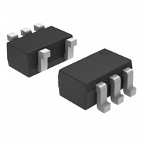
TSOT−23
TD SUFFIX
CASE 419AE
CAT823, CAT824
PIN CONNECTIONS
Description
The CAT823 and CAT824 provide basic reset and monitoring
functions for the electronic systems. Each device monitors the system
voltage and maintains a reset output until that voltage reaches the
device’s specified trip value and then maintains the reset output active
condition until the device’s internal timer, after a minimum timer of
140 ms; to allow the systems power supply to stabilize.
The CAT823 and CAT824 also have a watchdog input which can be
used to monitor a system signal and cause a reset to be issued if the
signal fails to change state prior to a timeout condition.
The CAT823 also provides a manual reset input which can be used
to initiate reset if pulled low. This input can be directly attached to
a push−button or a processor signal.
RESET
GND
•
•
•
•
CAT823
WDI
RESET
GND
1
VCC
CAT824
WDI
RESET
(Top Views)
Automatically Restarts Microprocessor after Power Failure
Monitors Pushbutton for External Override
Accurate Under Voltage System Monitoring
Brownout Detection System Reset for use with 3.0, 3.3, and 5.0 V
Systems
Pin and Function Compatible with the MAX823/24 Products
Operating Range from −40°C to +85°C
Available in TSOT−23 5−lead Package
These Devices are Pb−Free, Halogen Free/BFR Free and are RoHS
Compliant
Applications
•
•
•
•
•
VCC
MR
Features
•
•
•
•
1
MARKING DIAGRAM
XXXMG
G
XXX
M
G
= Specific Device Code
= Date Code
= Pb−Free Package*
(Note: Microdot may be in either location)
ORDERING INFORMATION
Microprocessor and Microcontroller Based Systems
Intelligent Instruments
Control Systems
Critical mP Monitors
Portable Equipment
See detailed ordering and shipping information in the package
dimensions section on page 9 of this data sheet.
PIN FUNCTIONS
Pin Name
RESET
GND
MR
RESET
Function
CMOS Push−Pull Active Low Reset Output
Ground
Manual Reset input – Pulled high Internally by a 52 kW
resistor designed to be driven low by a mechanical
pushbutton, open drain output or CMOS output.
CMOS Push−Pull Active High Reset Output
WDI
Watchdog Timer Input – Designed to be driven by a processor
output or can be disabled by tri−stating or leaving open.
VCC
Power Supply
© Semiconductor Components Industries, LLC, 2012
February, 2022 − Rev. 9
1
Publication Order Number:
CAT823/D
�CAT823, CAT824
WDI*
RESET
VCC
TOLERANCE
BIAS
VCC
VCC
VCC
TIMEOUT
COMPARATOR
LEVEL SENSE
&
TIMER
DIGITAL
DELAY
+
VCC
–
VOLTAGE
REFERENCE
RESET*
52 kW
LEVEL SENSE
&
DEBOUNCE
MR*
* Functions Available by Device
Figure 1. Block Diagram
Device
RESET
CAT823
x
CAT824
x
RESET
x
MR
WDI
x
x
x
Table 1. ABSOLUTE MAXIMUM RATINGS
Parameters
Ratings
Units
6
V
−0.3 to (VCC + 0.3)
V
Input Current, VCC
20
mA
Output Current RESET, RESET
20
Supply Voltage
All other pins
Continuous Power Dissipations (TA = +70°C)
TSOT−23 5−lead (derate 7.1 mW/°C above +70°C)
571
mA
mW
Storage Temperature
−65 to 150
°C
Operating Ambient Temperature
−40 to +85
°C
Lead Soldering (10 seconds max)
+300
°C
ESD Rating: Low Voltage Pins
Human Body Model
Machine Model
2000
200
V
Stresses exceeding those listed in the Maximum Ratings table may damage the device. If any of these limits are exceeded, device functionality
should not be assumed, damage may occur and reliability may be affected.
Table 2. RECOMMENDED OPERATING CONDITIONS
Parameter
Range
Units
VCC (TA = 0°C to +70°C)
1.0 to 5.5
V
VCC (TA = −40°C to +85°C)
1.2 to 5.5
V
All Other Pins
Ambient Temperature
www.onsemi.com
2
−0.1 to (VCC + 0.1)
V
−40 to +85
°C
�CAT823, CAT824
Table 3. ELECTRICAL OPERATING CHARACTERISTICS
(DC Characteristics: VCC = 3.0 V to 5.5 V for M version; VCC = 2.0 V to 3.6 V for the R/S/T/U/Y/Z version, −40°C ≤ TA ≤ +85°C unless
otherwise noted. Typical Values at TA = 25°C and VCC = 5 V for M version; VCC = 3.3 V for the T/S versions; VCC = 3.0 V for the R version;
and VCC = 2.5 V for the U/Y/Z versions.) (Note 1)
Symbol
ICC
VRST
Parameter
Supply Current
Reset Threshold
Conditions
Min
Typ
Max
Units
CAT824 (M Version)
6
17
mA
CAT823 (R/S/T/Y/Z Versions)
CAT824 (M/U Versions)
4
12
CAT82_M at −40°C ≤ TA ≤ +85°C
4.25
4.38
4.50
CAT82_T at −40°C ≤ TA ≤ +85°C
3.00
3.08
3.15
CAT82_S at −40°C ≤ TA ≤ +85°C
2.85
2.93
3.00
CAT82_R at −40°C ≤ TA ≤ +85°C
2.55
2.63
2.70
CAT82_Z at −40°C ≤ TA ≤ +85°C
2.25
2.32
2.38
CAT82_Y at −40°C ≤ TA ≤ +85°C
2.13
2.19
2.25
CAT824U at −40°C ≤ TA ≤ +85°C
1.95
2.00
2.05
Reset Threshold Tempco
Reset Threshold Hysteresis
tRD
VCC to Reset Delay (Note 2)
tRP
Reset Active Timeout Period
VOH
RESET Output High Voltage
40
ppm/°C
CAT82_M
10
mV
CAT82_R/S/T/Y/Z, CAT824U
5
VCC = VTH to (VTH − 100 mV)
20
140
CAT82_M, VCC = VRST max,
ISOURCE = −120 mA
CAT82_T/S/R/Z/Y, CAT824U,
VCC = VRST max, ISOURCE = −30 mA
VOL
ISOURCE
VOH
RESET Output Low Voltage
200
ms
400
ms
V
VCC − 1.5 V
0.8 x VCC
CAT82_M, VCC = VRST min,
ISINK = 3.2 mA
0.4
CAT82_T/S/R/Z/Y, CAT824U,
VCC = VRST min, ISINK = 1.2 mA
0.3
TA = 0°C to +70°C, VCC = 1 V,
VCC falling, ISINK = 50 mA
0.3
TA = TMIN to TMAX, VCC = 1.2 V,
VCC falling, ISINK = 100 mA
0.3
RESET Output
Short−Circuit Current
CAT82_M, Reset = 0 V, VCC = 5.5 V
1.5
CAT82_M, Reset = 0 V, VCC = 3.6 V
0.8
Reset Output Voltage
VCC > 1.8 V, ISOURCE = −150 mA
VOL
V
V
mA
V
0.8 x VCC
CAT824M, VCC = VRST max,
ISINK = 3.2 mA
0.4
CAT824M/U, VCC = VRST max,
ISINK = 1.2 mA
0.3
WATCHDOG INPUT (CAT823 & CAT824)
tWD
Watchdog Timeout Period
tWDI
WDI Pulse Width
VIL
WDI Input Voltage (Note 3)
1.12
VIL = 0.4 V, VIH = 0.8 x VCC
VIH
1.60
3.20
50
s
ns
0.3 x VCC
V
160
mA
0.7 x VCC
WDI Input Current (Note 4)
120
WDI = VCC, Time Average
WDI = 0 V, Time Average
www.onsemi.com
3
−20
−15
�CAT823, CAT824
Table 3. ELECTRICAL OPERATING CHARACTERISTICS (continued)
(DC Characteristics: VCC = 3.0 V to 5.5 V for M version; VCC = 2.0 V to 3.6 V for the R/S/T/U/Y/Z version, −40°C ≤ TA ≤ +85°C unless
otherwise noted. Typical Values at TA = 25°C and VCC = 5 V for M version; VCC = 3.3 V for the T/S versions; VCC = 3.0 V for the R version;
and VCC = 2.5 V for the U/Y/Z versions.) (Note 1)
Symbol
Parameter
Conditions
Min
Typ
Max
Units
0.3 x VCC
V
MANUAL RESET INPUT (CAT823)
MR Input Voltage
VIL
VIH
0.7 x VCC
tPB
MR Pulse Width
tPDLY
1
ms
MR low to Reset Delay
5
MR Noise Immunity
Pulse Width with No Reset
ms
100
MR Pullup Resistance
(internal)
35
52
ns
75
kW
Product parametric performance is indicated in the Electrical Characteristics for the listed test conditions, unless otherwise noted. Product
performance may not be indicated by the Electrical Characteristics if operated under different conditions.
1. Over−temperature limits are guaranteed by design and not production tested.
2. The RESET short−circuit current is the maximum pull−up current when reset is driven low by a bidirectional output.
3. WDI is internally serviced within the watchdog period if WDI is left open.
4. The WDI input current is specified as an average input current when the WDI input is driven high or low. The WDI input if connected to a
three−stated output device can be disabled in the tristate mode as long as the leakage current is less than 10 mA and a maximum capacitance
of less than 200 pF. To clock the WDI input in the active mode the drive device must be able to source or sink at least 200 mA when active.
TYPICAL ELECTRICAL OPERATING CHARACTERISTICS
NORMALIZED RESET THRESHOLD (V)
9
SUPPLY CURRENT (mA)
8
7
6
5
4
3
2
1
−40
−20
0
20
40
60
80
100
120
1.06
1.04
1.02
1.00
0.98
0.96
0.94
−40
−20
0
20
40
60
80
100
TEMPERATURE (°C)
TEMPERATURE (°C)
Figure 2. VCC Supply Current vs. Temperature
Figure 3. Normalized Reset Threshold Voltage
vs. Temperature
www.onsemi.com
4
�CAT823, CAT824
FUNCTIONAL DESCRIPTION
Processor RESET
Manual RESET
The CAT823 detects supply voltage (VCC) conditions that
are below the specified voltage trip value (VRST) and
provide a reset output to maintain correct system operation.
On power−up, RESET (and RESET if available) are kept
active for a minimum delay tRP of 140 ms after the supply
voltage (VCC) rises above VRST to allow the power supply
and processor to stabilize. When VCC drops below the
voltage trip value (VRST), the reset output signals RESET
(and RESET) are pulled active. RESET (and RESET if
available) is specifically designed to provide the reset input
signals for processors. This provides reliable and consistent
operation as power is turned on, off or during brownout
conditions by maintaining the processor operation in known
conditions.
The CAT823 has a Manual Reset (MR) input to allow for
alternative control of the reset outputs. The MR input is
designed for direct connection to a pushbutton (see
Figure 4). The MR input is internally pulled up by 52 kW
resistor and must be pulled low to cause the reset outputs to
go active. Internally, this input is debounced and timed such
that RESET (and RESET) signals of at least 140 ms
minimum will be generated. The min 140 ms tRP delay
commences as the Manual Reset input is released from the
low level (see Figure 5).
RESET
MR
Supply
Voltage
CAT823
VCC
GND
RESET
Figure 4. Pushbutton RESET
tPB
MR
tPDLY
VIH
VIL
tRP
RESET
VOH
VOL
RESET
Figure 5. Timing Diagram – Pushbutton RESET
www.onsemi.com
5
�CAT823, CAT824
Watchdog Timer
used to strobe the watchdog input. The most reliable is a
dedicated I/O output transitioned by a specific software
instruction.
The watchdog can be disabled by floating (or tri−stating)
the WDI input (see Figure 7). If the watchdog is disabled the
WDI pin will be pulled low for the first 7/8th’s of the
watchdog period (tWD) and pulled high for the last 1/8th of
the watchdog period. This pulling low of the WDI input and
then high is used to detect an open or tri−state condition and
will continue to repeat until the WDI input is driven high or
low.
For most efficient operation of devices with the watchdog
function the WDI input should be held low the majority of
the time and only strobed high as required to reset the
watchdog timer.
The CAT823 and CAT824 provide a Watchdog input
(WDI). The watchdog timer function forces RESET (and
RESET in the CAT824) signals active when the WDI input
does not have a transition from low−to−high or high−to−low
within 1.12 seconds. Timeout of the watchdog starts when
RESET (RESET on the CAT824) becomes inactive. If a
transition occurs on the WDI input pin prior to the watchdog
time−out, the watchdog timer is reset and begins to time−out
again. If the watchdog timer is allowed to time−out, then the
reset output(s) will go active for tRP and once released will
repeat the watchdog timeout process.
Figure 6 below shows a typical implementation of a
watchdog function. Any processor signal that repeats
dependant on the normal operation of the processor or
directed by the software operating on the processor can be
WDI
MR
Supply
Voltage
PIC
μC
GND
CAT823
VCC
RESET
DECODER
ADDRESS
MCLR
Figure 6. Watchdog Timer
VCC
Tristate
VCC
RESET
GND
mC
150 kW
CAT823
OUTPUT
MR
WDI
110 kW
Figure 7. Watchdog Disable Circuit
INVALID
STROBE
VALID
STROBE
INDETERMINATE
STROBE
WDI
tWD
MIN.
RESET
Figure 8. Timing Diagram – Strobe Input
www.onsemi.com
6
MAX.
�CAT823, CAT824
VCC
VRST (MAX)
VRST
VRST (MIN)
tRD
RESET
VOH
RESET Slews with VCC
VOL
RESET (CAT824)
Figure 9. Timing Diagram – Power Down
VRST (MAX)
VRST
VRST (MIN)
VCC
tRP
RESET
VOH
RESET
VOL
Figure 10. Timing Diagram – Power Up
www.onsemi.com
7
RESET (CAT824)
�CAT823, CAT824
Application Notes
Output Valid Conditions
The RESET output uses a push−pull output which can
maintain a valid output down to a VCC of 1.0 volts. To sink
current below 0.8 V a resistor can be connected from RESET
to Ground (see Figure 11.) This arrangement will maintain
a valid value on the RESET output during both power up and
down but will draw current when the RESET output is in the
high state. A resistor value of about 100 kW should be
adequate in most situations to maintain a low condition valid
output down to VCC equal to 0 V.
mP’s with Bidirectional Reset Pins
The RESET output can be pulled low by processors like
the 68HC11 allowing for a system reset issued by the
processor. The maximum pullup current that can be sourced
by the CAT82_M is 1.5 mA (and by the CAT82_T/R/S/Z/Y
is 800 mA) allowing the processor to pull the output low even
when the CAT82x is pulling it high.
Power Transients
Generally short duration negative−going transients of less
than 2 ms on the power supply at VRST minimum will not
cause a reset condition. However the lower the voltage of the
transient the shorter the required time to cause a reset output.
These issues can usually be remedied by the proper location
of bypass capacitance on the circuit board.
MR
WDI
CAT823
VCC
100 kW
GND
RESET
mC
RESET
Figure 11. RESET Valid to 0 Volts VCC
www.onsemi.com
8
�CAT823, CAT824
ORDERING INFORMATION
Order Number
NiPdAu
Top Mark
Inputs
Outputs
Voltage
NiPdAu
MR
WDI
RESET
RESET
CAT823TTDI−GT3
3.08 V
ETA
*
*
*
CAT823STDI−GT3
2.93 V
ETA
*
*
*
CAT823RTDI−GT3
2.63 V
ETA
*
*
*
CAT823ZTDI−GT3
2.32 V
ETA
*
*
*
CAT823YTDI−GT3
2.19 V
ETA
*
*
*
CAT824MTDI−GT3
4.38 V
EFA
*
*
*
CAT824UTDI−GT3
2.00 V
EFA
*
*
*
Package
Shipping†
TSOT−23−5
3,000 /
Tape & Reel
TOST−23−5
3,000 /
Tape & Reel
†For information on tape and reel specifications, including part orientation and tape sizes, please refer to our Tape and Reel Packaging
Specifications Brochure, BRD8011/D.
5. All packages are RoHS−compliant (Lead−free, Halogen−free).
6. The standard lead finish is NiPdAu.
7. Contact factory for package availability.
8. For detailed information and a breakdown of device nomenclature and numbering systems, please see the onsemi Device Nomenclature
document, TND310/D.
www.onsemi.com
9
�MECHANICAL CASE OUTLINE
PACKAGE DIMENSIONS
TSOT−23, 5 LEAD
CASE 419AE−01
ISSUE O
DATE 19 DEC 2008
SYMBOL
D
MIN
NOM
A
e
E1
MAX
1.00
A1
0.01
0.05
0.10
A2
0.80
0.87
0.90
b
0.30
c
0.12
E
0.45
0.15
D
2.90 BSC
E
2.80 BSC
E1
1.60 BSC
e
0.95 TYP
L
0.30
L1
0.40
0.20
0.50
0.60 REF
L2
0.25 BSC
0º
θ
8º
TOP VIEW
A2 A
b
q
L
A1
c
L2
L1
SIDE VIEW
END VIEW
Notes:
(1) All dimensions are in millimeters. Angles in degrees.
(2) Complies with JEDEC MO-193.
DOCUMENT NUMBER:
DESCRIPTION:
98AON34392E
TSOT−23, 5 LEAD
Electronic versions are uncontrolled except when accessed directly from the Document Repository.
Printed versions are uncontrolled except when stamped “CONTROLLED COPY” in red.
PAGE 1 OF 1
ON Semiconductor and
are trademarks of Semiconductor Components Industries, LLC dba ON Semiconductor or its subsidiaries in the United States and/or other countries.
ON Semiconductor reserves the right to make changes without further notice to any products herein. ON Semiconductor makes no warranty, representation or guarantee regarding
the suitability of its products for any particular purpose, nor does ON Semiconductor assume any liability arising out of the application or use of any product or circuit, and specifically
disclaims any and all liability, including without limitation special, consequential or incidental damages. ON Semiconductor does not convey any license under its patent rights nor the
rights of others.
© Semiconductor Components Industries, LLC, 2019
www.onsemi.com
�onsemi,
, and other names, marks, and brands are registered and/or common law trademarks of Semiconductor Components Industries, LLC dba “onsemi” or its affiliates
and/or subsidiaries in the United States and/or other countries. onsemi owns the rights to a number of patents, trademarks, copyrights, trade secrets, and other intellectual property.
A listing of onsemi’s product/patent coverage may be accessed at www.onsemi.com/site/pdf/Patent−Marking.pdf. onsemi reserves the right to make changes at any time to any
products or information herein, without notice. The information herein is provided “as−is” and onsemi makes no warranty, representation or guarantee regarding the accuracy of the
information, product features, availability, functionality, or suitability of its products for any particular purpose, nor does onsemi assume any liability arising out of the application or use
of any product or circuit, and specifically disclaims any and all liability, including without limitation special, consequential or incidental damages. Buyer is responsible for its products
and applications using onsemi products, including compliance with all laws, regulations and safety requirements or standards, regardless of any support or applications information
provided by onsemi. “Typical” parameters which may be provided in onsemi data sheets and/or specifications can and do vary in different applications and actual performance may
vary over time. All operating parameters, including “Typicals” must be validated for each customer application by customer’s technical experts. onsemi does not convey any license
under any of its intellectual property rights nor the rights of others. onsemi products are not designed, intended, or authorized for use as a critical component in life support systems
or any FDA Class 3 medical devices or medical devices with a same or similar classification in a foreign jurisdiction or any devices intended for implantation in the human body. Should
Buyer purchase or use onsemi products for any such unintended or unauthorized application, Buyer shall indemnify and hold onsemi and its officers, employees, subsidiaries, affiliates,
and distributors harmless against all claims, costs, damages, and expenses, and reasonable attorney fees arising out of, directly or indirectly, any claim of personal injury or death
associated with such unintended or unauthorized use, even if such claim alleges that onsemi was negligent regarding the design or manufacture of the part. onsemi is an Equal
Opportunity/Affirmative Action Employer. This literature is subject to all applicable copyright laws and is not for resale in any manner.
PUBLICATION ORDERING INFORMATION
LITERATURE FULFILLMENT:
Email Requests to: orderlit@onsemi.com
onsemi Website: www.onsemi.com
◊
TECHNICAL SUPPORT
North American Technical Support:
Voice Mail: 1 800−282−9855 Toll Free USA/Canada
Phone: 011 421 33 790 2910
Europe, Middle East and Africa Technical Support:
Phone: 00421 33 790 2910
For additional information, please contact your local Sales Representative
�