CM2009
VGA Port Companion
Circuit
Product Description
The CM2009 connects between a video graphics controller
embedded in a PC, graphics adapter card or set top box and the VGA
or DVI−I port connector. The CM2009 incorporates ESD protection
for all signals, level shifting for the DDC signals and buffering for the
SYNC signals. ESD protection for the video, DDC and SYNC lines is
implemented with low−capacitance current steering diodes.
All ESD diodes are designed to safely handle the high current spikes
specified by IEC−61000−4−2 Level 4 (±8 kV contact discharge if
CBYP is present, ±4 kV if not). The ESD protection for the DDC signal
pins are designed to prevent “back current” when the device is
powered down while connected to a monitor that is powered up.
Separate positive supply rails are provided for the VIDEO, DDC
and SYNC channels to facilitate interfacing with low voltage video
controller ICs to provide design flexibility in multi−supply−voltage
environments.
Two non−inverting drivers provide buffering for the HSYNC and
VSYNC signals from the video controller IC (SYNC1, SYNC2).
These buffers accept TTL input levels and convert them to CMOS
output levels that swing between Ground and VCC_SYNC, which is
typically 5 V. Additionally, each driver has a series termination resistor
(RT) connected to the SYNC_OUT pin, eliminating the external
termination resistors typically required for the HSYNC and VSYNC
lines of the video cable. There are three versions with different values
of RT to allow termination at typically 65 W (CM2009−00) or 15 W
(CM2009−02).
The 15 W (CM2009−02) version will typically require two external
resistors which can be chosen to exactly match the characteristic
impedance of the SYNC lines of the video cable.
Two N−channel MOSFETs provide the level shifting function
required when the DDC controller is operated at a lower supply
voltage than the monitor. The gate terminals for these MOSFETS
(VCC_DDC) should be connected to the supply rail (typically 3.3 V)
that supplies power to the transceivers of the DDC controller.
Features
• Includes ESD Protection, Level−Shifting, Buffering and
•
•
http://onsemi.com
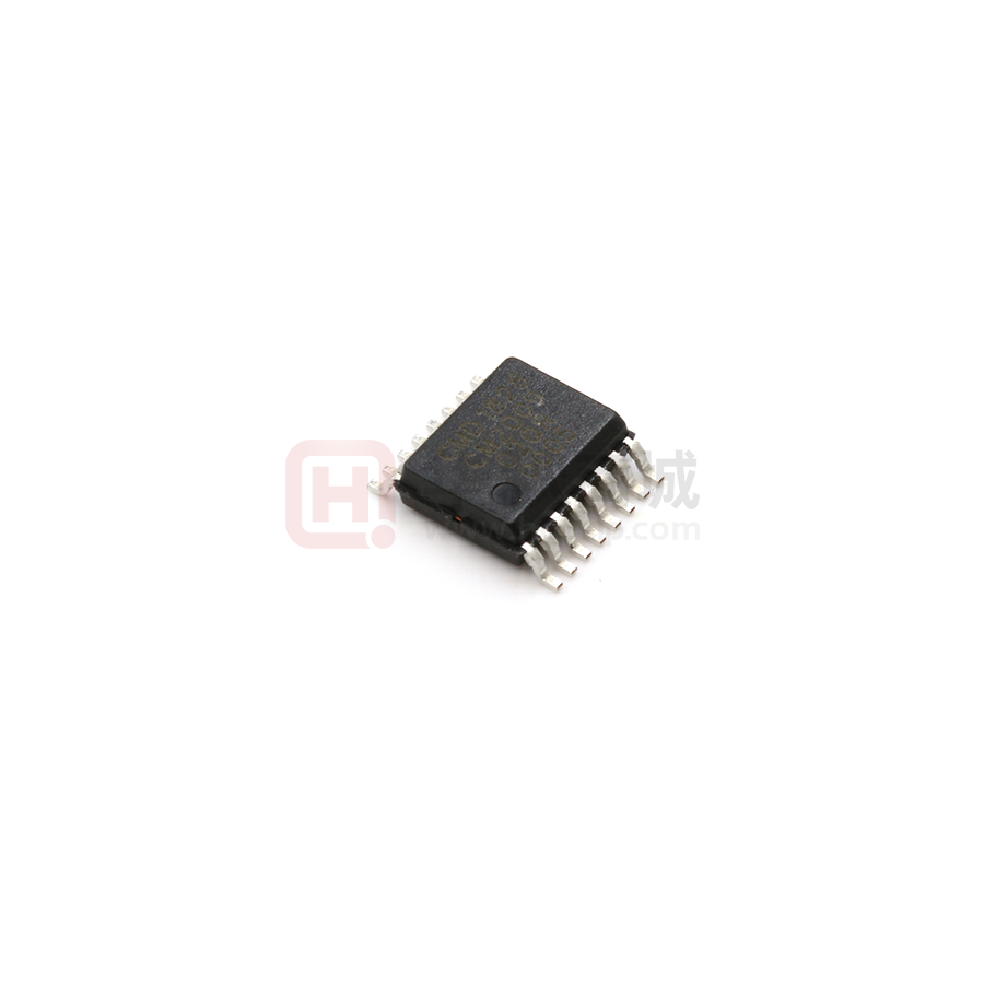
QSOP16
QR SUFFIX
CASE 492
MARKING DIAGRAM
CMD YYWW
CM2009
0xQR
CM2009 0xQR = Specific Device Code
YY
= Year
WW
= Work Week
ORDERING INFORMATION
Device
Package
Shipping†
CM2009−00QR
QSOP−16
(Pb−Free)
2500/Tape & Reel
CM2009−02QR
QSOP−16
(Pb−Free)
2500/Tape & Reel
†For information on tape and reel specifications,
including part orientation and tape sizes, please
refer to our Tape and Reel Packaging Specification
Brochure, BRD8011/D.
• 5 V Drivers for HSYNC and VSYNC Lines
• Integrated Impedance Matching Resistors on Sync Lines
• Bi−directional Level Shifting N−Channel FETs
Sync Impedance Matching
7 Channels of ESD Protection for all VGA Port
Connector Pins Meeting IEC−61000−4−2 Level 4 ESD
Requirements (±8 kV Contact Discharge)
Very Low Loading Capacitance from ESD Protection
Diodes on VIDEO Lines (4 pF Maximum)
Provided for DDC_CLK & DDC_DATA Channels
• Backdrive Protection on DDC Lines
• Compact 16−Lead QSOP Package
• These Devices are Pb−Free and are RoHS Compliant
Applications
• VGA and DVI−I Ports in:
♦
♦
♦
Desktop and Notebook PCs
Graphics Cards
Set Top Boxes
© Semiconductor Components Industries, LLC, 2012
May, 2012 − Rev. 5
1
Publication Order Number:
CM2009/D
�CM2009
SIMPLIFIED ELECTRICAL SCHEMATIC
9
VCC_VIDEO
2
12
VCC_DDC
VIDEO_1
VIDEO_2
VIDEO_3
GND
VCC_SYNC
BYP
8
7
DDC_OUT1
DDC_OUT2
1
3
4
5
RT
RT
6
16
14
DDC_IN1
DDC_IN2
10
SYNC_IN1
SYNC_IN2
13
15
GND
SYNC_OUT2
SYNC_OUT1
11
PACKAGE / PINOUT DIAGRAM
Top View
VCC_SYNC
1
16
SYNC_OUT2
VCC_VIDEO
2
15
SYNC_IN2
VIDEO_1
3
14
SYNC_OUT1
VIDEO_2
4
13
SYNC_IN1
VIDEO_3
5
12
DDC_OUT2
GND
6
11
DDC_IN2
VCC_DDC
7
10
DDC_IN1
BYP
8
9
DDC_OUT1
16 Pin QSOP
Table 1. PIN DESCRIPTIONS
Lead(s)
Name
1
VCC_SYNC
This is an isolated supply input for the SYNC_1 and SYNC_2 level shifters and their associated ESD
protection circuits.
2
VCC_VIDEO
This is a supply pin specifically for the VIDEO_1, VIDEO_2 and VIDEO_3 ESD protection circuits.
3
VIDEO_1
Video signal ESD protection channel. This pin is typically tied one of the video lines between the VGA
controller device and the video connector.
4
VIDEO_2
Video signal ESD protection channel. This pin is typically tied one of the video lines between the VGA
controller device and the video connector.
5
VIDEO_3
Video signal ESD protection channel. This pin is typically tied one of the video lines between the VGA
controller device and the video connector.
6
GND
7
VCC_DDC
8
BYP
9
DDC_OUT1
10
DDC_IN1
Description
Ground reference supply pin.
This is an isolated supply input for the DDC_1 and DDC_2 level−shifting N−FET gates.
This input is used to connect an external 0.2 mF bypass capacitor to the DDC circuits, resulting in an
increased ESD withstand voltage rating for these circuits (±8 kV with vs. ±4 kV without).
DDC signal output. Connects to the video connector side of one of the sync lines.
DDC signal input. Connects to the VGA controller side of one of the sync lines.
http://onsemi.com
2
�CM2009
Table 1. PIN DESCRIPTIONS
Lead(s)
Name
11
DDC_IN2
Description
12
DDC_OUT2
DDC signal output. Connects to the video connector side of one of the sync lines.
13
SYNC_IN1
Sync signal buffer input. Connects to the VGA controller side of one of the sync lines.
14
SYNC_OUT1
15
SYNC_IN2
16
SYNC_OUT2
DDC signal input. Connects to the VGA controller side of one of the sync lines.
Sync signal buffer output. Connects to the video connector side of one of the sync lines.
Sync signal buffer input. Connects to the VGA controller side of one of the sync lines.
Sync signal buffer output. Connects to the video connector side of one of the sync lines.
SPECIFICATIONS
Table 2. ABSOLUTE MAXIMUM RATINGS
Parameter
VCC_VIDEO, VCC_DDC and VCC_SYNC Supply Voltage Inputs
ESD Diode Forward Current (one diode conducting at a time)
DC Voltage at Inputs
VIDEO_1, VIDEO_2, VIDEO_3
DDC_IN1, DDC_IN2
DDC_OUT1, DDC_OUT2
SYNC_IN1, SYNC_IN2
Rating
Units
[GND − 0.5] to +6.0
V
10
mA
[GND − 0.5] to [VCC_VIDEO + 0.5]
[GND − 0.5] to 6.0
[GND − 0.5] to 6.0
[GND − 0.5] to [VCC_SYNC + 0.5]
V
Operating Temperature Range
−40 to +85
Storage Temperature Range
−40 to +150
°C
500
mW
Package Power Rating (TA = 25°C)
°C
Stresses exceeding Maximum Ratings may damage the device. Maximum Ratings are stress ratings only. Functional operation above the
Recommended Operating Conditions is not implied. Extended exposure to stresses above the Recommended Operating Conditions may affect
device reliability.
http://onsemi.com
3
�CM2009
Table 3. ELECTRICAL OPERATING CHARACTERISTICS (Note 1)
Symbol
Max
Units
VCC_VIDEO Supply Current
VCC_VIDEO = 5.0 V; VIDEO inputs at VCC_VIDEO
or GND
10
mA
ICC_DDC
VCC_DDC Supply Current
VCC_DDC = 5.0 V
10
mA
ICC_SYNC
VCC_SYNC Supply Current
VCC_SYNC = 5 V; SYNC inputs at GND or
VCC_SYNC; SYNC outputs unloaded
50
mA
VCC_SYNC = 5 V; SYNC inputs at 3.0 V;
SYNC outputs unloaded
2.0
mA
1.0
V
ICC_VIDEO
Parameter
Conditions
Min
Typ
VF
ESD Diode Forward Voltage
IF = 10 mA
VIH
Logic High Input Voltage
VCC_SYNC = 5.0 V; (Note 2)
VIL
Logic Low Input Voltage
VCC_SYNC = 5.0 V; (Note 2)
VOH
Logic High Output Voltage
IOH = 0 mA, VCC_SYNC = 5.0 V; (Note 2)
VOL
Logic Low Output Voltage
IOL = 0 mA, VCC_SYNC = 5.0 V; (Note 2)
ROUT
SYNC Driver Output Resistance
(CM2009−00 only)
VCC_SYNC = 5.0 V; SYNC Inputs at GND or 3.0 V
65
W
ROUT
SYNC Driver Output Resistance
(CM2009−02 only)
VCC_SYNC = 5.0 V; SYNC Inputs at GND or 3.0 V;
(Note ?)
15
W
VOH−02
Logic High Output Voltage
(CM2009−02 only)
IOH = 24 mA; VCC_SYNC = 5.0 V;
(Note 2)
VOL−02
Logic Low Output Voltage
(CM2009−02 only)
IOL = 24 mA; VCC_SYNC = 5.0 V;
(Note 2)
0.8
V
Input Current
VIDEO Inputs
VCC_VIDEO = 5.0 V; VIN = VCC_VIDEO or GND
±1
mA
VCC_SYNC = 5.0 V; VIN = VCC_SYNC or GND
±1
mA
(VCC_DDC − VDDC_IN) ≤ 0.4 V;
VDDC_OUT = VCC_DDC
10
mA
(VCC_DDC − VDDC_OUT) ≤ 0.4 V;
VDDC_IN = VCC_DDC
10
mA
IIN
SYNC_IN1, SYNC_IN2 Inputs
IOFF
VON
CIN_VID
Level Shifting N−MOSFET ”OFF” State
Leakage Current
2.0
V
0.6
4.85
V
V
0.15
2.0
V
V
Voltage Drop Across Level−shifting
N−MOSFET when “ON”
VCC_DDC = 2.5 V; VS = GND; IDS = 3 mA;
0.18
V
VIDEO Input Capacitance
VCC_VIDEO = 5.0 V; VIN = 2.5 V; f = 1 MHz;
(Note 4)
4
pF
VCC_VIDEO = 2.5 V; VIN = 1.25 V; f = 1 MHz;
(Note 4)
4.5
pF
tPLH
SYNC Driver L => H Propagation Delay
CL = 50 pF; VCC = 5.0 V; Input tR and tF ≤ 5 ns
12
ns
tPHL
SYNC Driver H => L Propagation Delay
CL = 50 pF; VCC = 5.0 V; Input tR and tF ≤ 5 ns
12
ns
tR, tF
SYNC Driver Output Rise & Fall Times
CL = 50 pF; VCC = 5.0 V; Input tR and tF ≤ 5 ns
VESD
ESD Withstand Voltage
VCC_VIDEO = VCC_SYNC = 5 V; (Notes 3, 4 & ?)
4
±8
ns
kV
1. All parameters specified over standard operating conditions unless otherwise noted.
2. These parameters apply only to the SYNC drivers. Note that ROUT = RT + RBUFFER.
3. Per the IEC−61000−4−2 International ESD Standard, Level 4 contact discharge method. BYP, VCC_VIDEO and VCC_SYNC must be bypassed
to GND via a low impedance ground plane with a 0.2 mF, low inductance, chip ceramic capacitor at each supply pin. ESD pulse is applied
between the applicable pins and GND. ESD pulses can be positive or negative with respect to GND. Applicable pins are: VIDEO_1, VIDEO_2,
VIDEO_3, SYNC_OUT1, SYNC_OUT2, DDC_OUT1 and DDC_OUT2. All other pins are ESD protected to the industry standard ±2 kV
Human Body Model (MIL−STD−883, Method 3015). The bypass capacitor at the BYP pin may optionally be omitted, in which case the max.
ESD withstand voltage for the DDC_OUT1 and DDC_OUT2 pins is reduced to ±4 kV.
4. The SYNC_OUT pins on the CM2009−02 are guaranteed for 2 kV HBM ESD protection.
http://onsemi.com
4
�CM2009
APPLICATION INFORMATION
Figure 1. Typical Application Connection Diagram
NOTES:
1. The CM2009 should be placed as close to the VGA or DVI−I connector as possible.
2. The ESD protection channels VIDEO_1, VIDEO_2, VIDEO_3 may be used interchangeably between the R, G, B
signals.
3. If differential video signal routing is used, the RED, BLUE, and GREEN signal lines should be terminated with
external 37.5 W resistors.
4. “VF” are external video filters for the RGB signals.
5. Supply bypass capacitors C1 and C2 must be placed immediately adjacent to the corresponding Vcc pins.
Connections to the Vcc pins and ground plane must be made with minimal length copper traces (preferably less than
5 mm) for best ESD protection.
6. The bypass capacitor for the BYP pin has been omitted in this diagram. This results in a reduction in the maximum
ESD withstand voltage at the DDC_OUT pins from ±8 kV to ±4 kV. If 8 kV ESD protection is required, a 0.2 mF
ceramic bypass capacitor should be connected between BYP and ground.
7. The SYNC buffers may be used interchangeably between HSYNC and VSYNC.
8. The EMI filters at the SYNC_OUT and DDC_OUT pins (C5 to C12, and Ferrite Beads FB1 to FB4) are for reference
only. The component values and filter configuration may be changed to suit the application.
9. The DDC level shifters DDC_IN, DDC_OUT, may be used interchangeably between DDCA_CLK and
DDCA_DATA.
10. R1, R2 are optional. They may be used, if required, to pull the DDC_CLK and DDC_DATA lines to VCC_5V when
no monitor is connected to the VGA connector. If used, it should be noted that “back current” may flow between the
DDC pins and VCC_5V via these resistors when VCC_5V is powered down.
11. For optimal ESD performance with the CM2009−02, an additional clamp device (such as the CMD PACDN042)
should be placed on HSYNC/VSYNC lines between the external matching resistor and the VGA connector.
http://onsemi.com
5
�MECHANICAL CASE OUTLINE
PACKAGE DIMENSIONS
QSOP16
CASE 492−01
ISSUE A
DATE 23 MAR 2011
2X
SCALE 2:1
NOTES:
1. DIMENSIONING AND TOLERANCING PER ASME
Y14.5M, 1994.
2. CONTROLLING DIMENSION: MILLIMETERS.
3. DIMENSION b DOES NOT INCLUDE DAMBAR
PROTRUSION.
4. DIMENSION D DOES NOT INCLUDE MOLD FLASH,
PROTRUSIONS, OR GATE BURRS. MOLD FLASH,
PROTRUSIONS, OR GATE BURRS SHALL NOT EX
CEED 0.005 PER SIDE. DIMENSION E1 DOES NOT
INCLUDE INTERLEAD FLASH OR PROTRUSION. IN
TERLEAD FLASH OR PROTRUSION SHALL NOT EX
CEED 0.005 PER SIDE. D AND E1 ARE DETERMINED
AT DATUM H.
5. DATUMS A AND B ARE DETERMINED AT DATUM H.
0.20 C D
D
16
L2
D
A
9
GAUGE
PLANE
SEATING
PLANE
E
E1
C
L
C
DETAIL A
2X
2X 10 TIPS
0.20 C D
1
8
16X
e
B
b
0.25
A2
0.10 C
0.10 C
A1
16X
C
0.25 C D
M
C A-B D
h x 45 _
A
SEATING
PLANE
M
1.12
9
XXXXXXX
XXXXXXX
YYWWG
6.40
1
8
0.635
PITCH
DOCUMENT NUMBER:
DESCRIPTION:
MILLIMETERS
MIN
MAX
1.35
1.75
0.10
0.25
1.24
---0.20
0.30
0.19
0.25
4.89 BSC
6.00 BSC
3.90 BSC
0.635 BSC
0.22
0.50
0.40
1.27
0.25 BSC
0_
8_
16X
0.42
16
DETAIL A
INCHES
MIN
MAX
0.053
0.069
0.004
0.010
0.049
---0.008
0.012
0.007
0.010
0.193 BSC
0.237 BSC
0.154 BSC
0.025 BSC
0.009
0.020
0.016
0.050
0.010 BSC
0_
8_
GENERIC
MARKING DIAGRAM*
SOLDERING FOOTPRINT
16X
H
DIM
A
A1
A2
b
c
D
E
E1
e
h
L
L2
M
XXXXX
YY
WW
G
= Specific Device Code
= Year
= Work Week
= Pb−Free Package
*This information is generic. Please refer
to device data sheet for actual part
marking. Pb−Free indicator, “G”, may
or not be present.
DIMENSIONS: MILLIMETERS
98AON04472D
QSOP16
Electronic versions are uncontrolled except when accessed directly from the Document Repository.
Printed versions are uncontrolled except when stamped “CONTROLLED COPY” in red.
PAGE 1 OF 1
ON Semiconductor and
are trademarks of Semiconductor Components Industries, LLC dba ON Semiconductor or its subsidiaries in the United States and/or other countries.
ON Semiconductor reserves the right to make changes without further notice to any products herein. ON Semiconductor makes no warranty, representation or guarantee regarding
the suitability of its products for any particular purpose, nor does ON Semiconductor assume any liability arising out of the application or use of any product or circuit, and specifically
disclaims any and all liability, including without limitation special, consequential or incidental damages. ON Semiconductor does not convey any license under its patent rights nor the
rights of others.
© Semiconductor Components Industries, LLC, 2019
www.onsemi.com
�onsemi,
, and other names, marks, and brands are registered and/or common law trademarks of Semiconductor Components Industries, LLC dba “onsemi” or its affiliates
and/or subsidiaries in the United States and/or other countries. onsemi owns the rights to a number of patents, trademarks, copyrights, trade secrets, and other intellectual property.
A listing of onsemi’s product/patent coverage may be accessed at www.onsemi.com/site/pdf/Patent−Marking.pdf. onsemi reserves the right to make changes at any time to any
products or information herein, without notice. The information herein is provided “as−is” and onsemi makes no warranty, representation or guarantee regarding the accuracy of the
information, product features, availability, functionality, or suitability of its products for any particular purpose, nor does onsemi assume any liability arising out of the application or use
of any product or circuit, and specifically disclaims any and all liability, including without limitation special, consequential or incidental damages. Buyer is responsible for its products
and applications using onsemi products, including compliance with all laws, regulations and safety requirements or standards, regardless of any support or applications information
provided by onsemi. “Typical” parameters which may be provided in onsemi data sheets and/or specifications can and do vary in different applications and actual performance may
vary over time. All operating parameters, including “Typicals” must be validated for each customer application by customer’s technical experts. onsemi does not convey any license
under any of its intellectual property rights nor the rights of others. onsemi products are not designed, intended, or authorized for use as a critical component in life support systems
or any FDA Class 3 medical devices or medical devices with a same or similar classification in a foreign jurisdiction or any devices intended for implantation in the human body. Should
Buyer purchase or use onsemi products for any such unintended or unauthorized application, Buyer shall indemnify and hold onsemi and its officers, employees, subsidiaries, affiliates,
and distributors harmless against all claims, costs, damages, and expenses, and reasonable attorney fees arising out of, directly or indirectly, any claim of personal injury or death
associated with such unintended or unauthorized use, even if such claim alleges that onsemi was negligent regarding the design or manufacture of the part. onsemi is an Equal
Opportunity/Affirmative Action Employer. This literature is subject to all applicable copyright laws and is not for resale in any manner.
PUBLICATION ORDERING INFORMATION
LITERATURE FULFILLMENT:
Email Requests to: orderlit@onsemi.com
onsemi Website: www.onsemi.com
◊
TECHNICAL SUPPORT
North American Technical Support:
Voice Mail: 1 800−282−9855 Toll Free USA/Canada
Phone: 011 421 33 790 2910
Europe, Middle East and Africa Technical Support:
Phone: 00421 33 790 2910
For additional information, please contact your local Sales Representative
�


 工商网监
湘ICP备2023018690号
工商网监
湘ICP备2023018690号

