ON Semiconductor
Is Now
To learn more about onsemi™, please visit our website at
www.onsemi.com
onsemi and and other names, marks, and brands are registered and/or common law trademarks of Semiconductor Components Industries, LLC dba “onsemi” or its affiliates and/or
subsidiaries in the United States and/or other countries. onsemi owns the rights to a number of patents, trademarks, copyrights, trade secrets, and other intellectual property. A listing of onsemi
product/patent coverage may be accessed at www.onsemi.com/site/pdf/Patent-Marking.pdf. onsemi reserves the right to make changes at any time to any products or information herein, without
notice. The information herein is provided “as-is” and onsemi makes no warranty, representation or guarantee regarding the accuracy of the information, product features, availability, functionality,
or suitability of its products for any particular purpose, nor does onsemi assume any liability arising out of the application or use of any product or circuit, and specifically disclaims any and all
liability, including without limitation special, consequential or incidental damages. Buyer is responsible for its products and applications using onsemi products, including compliance with all laws,
regulations and safety requirements or standards, regardless of any support or applications information provided by onsemi. “Typical” parameters which may be provided in onsemi data sheets and/
or specifications can and do vary in different applications and actual performance may vary over time. All operating parameters, including “Typicals” must be validated for each customer application
by customer’s technical experts. onsemi does not convey any license under any of its intellectual property rights nor the rights of others. onsemi products are not designed, intended, or authorized
for use as a critical component in life support systems or any FDA Class 3 medical devices or medical devices with a same or similar classification in a foreign jurisdiction or any devices intended for
implantation in the human body. Should Buyer purchase or use onsemi products for any such unintended or unauthorized application, Buyer shall indemnify and hold onsemi and its officers, employees,
subsidiaries, affiliates, and distributors harmless against all claims, costs, damages, and expenses, and reasonable attorney fees arising out of, directly or indirectly, any claim of personal injury or death
associated with such unintended or unauthorized use, even if such claim alleges that onsemi was negligent regarding the design or manufacture of the part. onsemi is an Equal Opportunity/Affirmative
Action Employer. This literature is subject to all applicable copyright laws and is not for resale in any manner. Other names and brands may be claimed as the property of others.
�CMPWR101
250 mA SmartORt Regulator
with VAUX Switch
Product Description
The ON Semiconductor’s SmartORt CMPWR101 is a low dropout
regulator that delivers up to 250 mA of load current at a fixed 3.3 V
output. An internal threshold level (typically 4.1 V) is used to prevent
the regulator from being operated below dropout voltage. The device
continuously monitors the input supply and will automatically disable
the regulator when VCC falls below the threshold level. When the
regulator is disabled, a low impedance, fully integrated switch is
enabled which allows the output to be directly powered from an
auxiliary 3.3 V supply.
When VCC is restored to a level above the select threshold, the low
impedance switch is disabled and the regulator is once again enabled.
All the necessary control circuitry needed to provide a smooth and
automatic transition between the supplies has been incorporated. This
allows VCC to be dynamically switched without loss of output voltage.
An output logic signal, DRIVE, is active LOW whenever the
internal regulator is disabled.
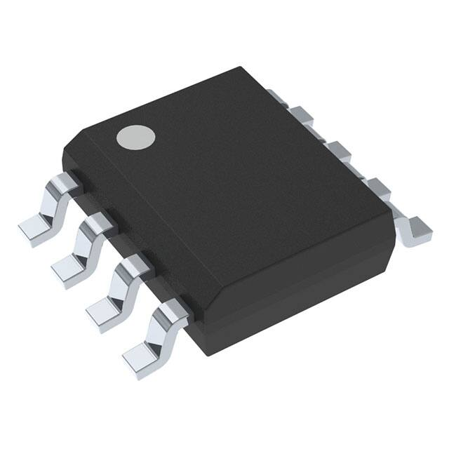
The CMPWR101 is housed in a 8−pin SOIC package and is
available with RoHS compliant lead−free finishing.
Features
•
•
•
•
•
•
•
•
•
•
http://onsemi.com
SIOC 8
R SUFFIX
CASE 751BD
MARKING DIAGRAM
CMPWR 101R
CMPWR 101R = CMPWR101R
Automatic Detection of VCC Input Supply
Glitch−Free Output During Supply Transitions
Built−In Hysteresis During Supply Selection
250 mA Output Maximum Load Current
Fully Integrated VAUX Switch
Overload Current Protection
Short Circuit Current Protection
Operates from Either VCC or VAUX
8−Pin SOIC Package
These Devices are Pb−Free and are RoHS Compliant
ORDERING INFORMATION
Device
Package
Shipping†
CMPWR101R
SOIC
(Pb−Free)
2500/Tape & Reel
†For information on tape and reel specifications,
including part orientation and tape sizes, please
refer to our Tape and Reel Packaging Specification
Brochure, BRD8011/D.
Applications
•
•
•
•
PCI Adapter Cards
Network Interface Cards (NICs)
Dual Power Systems
Systems with Standby Capabilities
© Semiconductor Components Industries, LLC, 2011
April, 2011 − Rev. 4
1
Publication Order Number:
CMPWR101/D
�CMPWR101
TYPICAL APPLICATION CIRCUIT
SIMPLIFIED ELECTRICAL SCHEMATIC
VCC
CMPWR101
5V
VCC
VAUX
+ CIN
3.3 V
1 mF
VCC
DRIVE
VAUX
VOUT
GND
+
VDESELECT -
DRIVE
3.3 V/250 mA
0.2 W
+ COUT
VREF
3.3 V
-
VOUT
VAUX
4 mF
DRIVE
+
4.1 V
VOUT
ENABLE
GND
GND
PACKAGE / PINOUT DIAGRAM
Top View
VCC
1
8
DRIVE
VAUX
2
7
VOUT
VAUX
3
6
VOUT
GND
4
5
N/C
8−Pin SOIC
Table 1. PIN DESCRIPTIONS
Pin(s)
Name
Description
1
VCC
VCC is the power source for the internal regulator and is monitored continuously by an internal controller
circuit. Whenever VCC exceeds VCCSEL (4.25 V typically), the internal regulator will be enabled and deliver
a fixed 3.3 V at VOUT.
When VCC falls below VCCDES (4.10 V typically), the regulator will be disabled. Internal loading on this pin is
typically 0.6 mA when the regulator is enabled, which reduces to 0.1 mA whenever the regulator is disabled. If
VCC falls below the voltage on the VAUX pin, the VCC loading will further reduce to only a few microamperes.
During a VCC power−up or power−down sequence, there will be an effective step increase in VCC line current
when the regulator is enabled/disabled. This line current transient will cause a voltage disturbance at the VCC
pin. The magnitude of the disturbance will be directly proportional to the effective power supply source
impedance being delivered to the VCC input.
A built−in hysteresis voltage of 150 mV has been incorporated to minimize any chatter during supply
changeover. It is recommended that the power supply connected to the VCC input should have a source
resistance of less than 0.25 W to minimize the event of chatter during the enabling/disabling of the regulator.
If the VCC pin is within a few inches of the main input filter, a capacitor may not be necessary. Otherwise an
input filter capacitor in the range of 1 mF to 10 mF will help to lower the effective source impedance.
2−3
VAUX
VAUX is the auxiliary power source. When selected, (VCC < VCCDES), the auxiliary supply is directly connected
to VOUT, via the low impedance (0.3 W typically) fully integrated switch.
The internal loading on this pin is typically less than 10 mA and will increase to 100 mA if VCC falls below the
voltage on VAUX.
When VAUX = 0 V, the VCCDES voltage is inhibited which prevents the regulator from being disabled.
4
GND
GND is the negative reference for all voltages. The current that flows in the ground connection is very low
(typically 0.6 mA) and has minimal variation over all load conditions.
5
NC
6−7
VOUT
8
DRIVE
NC is an unconnected pin which is electrically isolated from the internal circuitry.
VOUT is the regulator output voltage connection used to power the load. An output capacitor of 4.7 mF is used
to provide the necessary phase compensation, thereby preventing oscillation. The capacitor also helps to
minimize the peak output disturbance during power supply changeover.
DRIVE is a CMOS output logic signal (Active Low) referenced to the VCC supply. This output is taken low
whenever the internal regulator is not enabled. This output is intended only as a control signal for external
circuitry.
http://onsemi.com
2
�CMPWR101
SPECIFICATIONS
Table 2. ABSOLUTE MAXIMUM RATINGS
Parameter
ESD Protection (HBM)
Pin Input Voltages
VCC
VAUX
DRIVE
Rating
Units
±2000
V
V
[GND − 0.5] to +6.0
[GND − 0.5] to +4.0
[GND − 0.5] to [VCC + 0.5]
Storage Temperature Range
−40 to +150
Operating Temperature Range
Ambient
Junction
°C
°C
0 to +70
0 to +125
Power Dissipation (Note 1)
0.5
W
Stresses exceeding Maximum Ratings may damage the device. Maximum Ratings are stress ratings only. Functional operation above the
Recommended Operating Conditions is not implied. Extended exposure to stresses above the Recommended Operating Conditions may affect
device reliability.
1. The power rating is based on a printed circuit board heat spreading capability equivalent to 2 square inches of copper connected to the GND
pins. Typical multi−layer boards using power plane construction will provide this heat spreading ability without the need for additional
dedicated copper area. (Please consult with factory for thermal evaluation assistance).
Table 3. STANDARD OPERATING CONDITIONS
Parameter
Rating
Units
VCC
5.0 ±0.5
V
VAUX
3.3 ±0.3
V
Ambient Operating Temperature Range
0 to +70
°C
Load Current
0 to 250
mA
CEXT
4.7 ±20%
mF
Table 4. ELECTRICAL OPERATING CHARACTERISTICS (Note 2)
Symbol
VOUT
ILIM
Parameter
Regulator Output Voltage
Conditions
0 mA < ILOAD < 250 mA
Regulator Current Limit
Min
Typ
Max
3.135
3.300
3.465
275
VCCSEL
VCC Select Voltage
Regulator Enabled
VCCDES
VCC Deselect Voltage
Regulator Disabled
VCCHYST
Hysteresis Voltage
(Note 3)
VR LOAD
Load Regulation
VCC = 5 V, 5 mA < ILOAD < 250 mA
VR LINE
Line Regulation
ILOAD = 5 mA; 4.5 V < VCC < to 5.5 V
RSW
VAUX Switch Resistance
VCCDES > VCC, VAUX = 3.3 V
IRCC
IRAUX
VCC Reverse Leakage
VAUX Reverse Leakage
VAUX = 3.3 V, VCC = 0 V
VAUX = 0 V, VCC = 5 V
IGND
Ground Current
IAUX
V
mA
4.30
3.90
Units
4.45
V
4.10
V
0.20
V
20
mV
2
mV
0.25
0.40
W
2
2
50
50
mA
VCC < VCCDES, ILOAD = 0 mA
VCC > VCCSEL, ILOAD = 0 mA
VCC > VCCSEL, ILOAD = 250 mA
0.20
0.60
0.70
0.40
1.00
1.20
mA
VAUX Supply Current
VAUX > VCC
VCC > VAUX
0.20
0.02
0.40
0.10
mA
ROH
DRIVE Pull−up Resistance
RPULLUP to VCC, VCC > VCCSEL
4.0
8.0
kW
ROL
DRIVE Pull−down Resistance
RPULLDOWN to GND, VCCDES > VCC
0.1
0.4
kW
2. Operating Characteristics are over Standard Operating Conditions unless otherwise specified.
3. The hysteresis defines the maximum level of acceptable disturbance on VCC during switching. It is recommended that the VCC source
impedance be kept below 0.25 W to ensure the switching disturbance remains below the hysteresis during select/deselect transitions. An
input capacitor may be required to help minimize the switching transient.
http://onsemi.com
3
�CMPWR101
PERFORMANCE INFORMATION
CMPWR101 Typical DC Characteristics (nominal conditions unless specified otherwise)
Figure 1. Supply Current vs. Voltage
(VAUX = 3.3 V)
Figure 2. Switch Resistance vs. Supply Voltage
Figure 3. Ground Current vs. Output Load
Figure 4. Line Regulation
(1% and 100& Rated Load)
Figure 5. Load Regulation
Figure 6. Dropout Voltage with Load Current
http://onsemi.com
4
�CMPWR101
PERFORMANCE INFORMATION (Cont’d)
CMPWR101 Transient Characteristics (nominal conditions unless specified otherwise)
(VCC source resistance set to 0.2 W)
Figure 7. VCC Cold Start Power Up
(VAUX = 0 V)
Figure 8. VCC Complete Power Down
(VAUX = 0 V)
Figure 9. VCC Power Up
(VAUX = 3.3 V)
Figure 10. VCC Power Down
(VAUX = 3.3 V)
Figure 11. Load Transient (10% to 90%)
Step Response
Figure 12. Line Transient (1 VPP)
Step Response
http://onsemi.com
5
�CMPWR101
PERFORMANCE INFORMATION (Cont’d)
CMPWR101 Typical Thermal Characteristics
The overall junction to ambient thermal resistance (qJA)
for device power dissipation (PD) consists primarily of two
paths in series. The first path is the junction to the case (qJC)
which is defined by the package style, and the second path
is case to ambient (qCA) thermal resistance which is
dependent on board layout. The final operating junction
temperature for any set of conditions can be estimated by the
following thermal equation:
T JUNC + T AMB ) P D(q JC) ) P D(q CA)
+ T AMB ) P D(q JA)
The CMPWR101 uses a standard SOIC package. When
this package is mounted on a double−sided printed circuit
board with two square inches of copper allocated for “heat
spreading”, the resulting qJA is 85°C/W.
Based on a maximum power dissipation of 0.43 W
(1.7 V x 250 mA) with an ambient of 70°C, the resulting
junction temperature will be:
Figure 13. Regulator VOUT vs. TAMB (250 mA Load)
T JUNC + T AMB ) P D(q JA)
+ 70° C ) 0.4�W�(80° CńD)
+ 70° C ) 37° C + 103° C
Thermal characteristics were measured using
a double−sided board with two square inches of copper area
connected to the GND pin for “heat spreading”.
Measurements showing performance up to junction
temperature of 125°C were performed under light load
conditions (5 mA). This allows the ambient temperature to
be representative of the internal junction temperature.
NOTE: Note: The use of multi−layer board construction
with separate ground and power planes will
further enhance the overall thermal
performance. In the event of no copper area
being dedicated for heat spreading, a multi−layer
board construction, using only the minimum size
pad layout, will provide the CMPWR101 with
an overall qJA of 100°C/W which allows up to
500 mW to be safely dissipated.
Figure 14. Deselect Threshold vs. TJUNCT
Figure 15. Switch Resistance vs. Ambient
Temperature
http://onsemi.com
6
�CMPWR101
PACKAGE DIMENSIONS
SOIC 8, 150 mils
CASE 751BD−01
ISSUE O
E1
E
SYMBOL
MIN
A
1.35
1.75
A1
0.10
0.25
b
0.33
0.51
c
0.19
0.25
D
4.80
5.00
E
5.80
6.20
E1
3.80
4.00
MAX
1.27 BSC
e
PIN # 1
IDENTIFICATION
NOM
h
0.25
0.50
L
0.40
1.27
θ
0º
8º
TOP VIEW
D
h
A1
θ
A
c
e
b
L
SIDE VIEW
END VIEW
Notes:
(1) All dimensions are in millimeters. Angles in degrees.
(2) Complies with JEDEC MS-012.
SmartOR is a trademark of Semiconductor Components Industries, LLC (SCILLC).
ON Semiconductor and
are registered trademarks of Semiconductor Components Industries, LLC (SCILLC). SCILLC reserves the right to make changes without further notice
to any products herein. SCILLC makes no warranty, representation or guarantee regarding the suitability of its products for any particular purpose, nor does SCILLC assume any liability
arising out of the application or use of any product or circuit, and specifically disclaims any and all liability, including without limitation special, consequential or incidental damages.
“Typical” parameters which may be provided in SCILLC data sheets and/or specifications can and do vary in different applications and actual performance may vary over time. All
operating parameters, including “Typicals” must be validated for each customer application by customer’s technical experts. SCILLC does not convey any license under its patent rights
nor the rights of others. SCILLC products are not designed, intended, or authorized for use as components in systems intended for surgical implant into the body, or other applications
intended to support or sustain life, or for any other application in which the failure of the SCILLC product could create a situation where personal injury or death may occur. Should
Buyer purchase or use SCILLC products for any such unintended or unauthorized application, Buyer shall indemnify and hold SCILLC and its officers, employees, subsidiaries, affiliates,
and distributors harmless against all claims, costs, damages, and expenses, and reasonable attorney fees arising out of, directly or indirectly, any claim of personal injury or death
associated with such unintended or unauthorized use, even if such claim alleges that SCILLC was negligent regarding the design or manufacture of the part. SCILLC is an Equal
Opportunity/Affirmative Action Employer. This literature is subject to all applicable copyright laws and is not for resale in any manner.
PUBLICATION ORDERING INFORMATION
LITERATURE FULFILLMENT:
Literature Distribution Center for ON Semiconductor
P.O. Box 5163, Denver, Colorado 80217 USA
Phone: 303−675−2175 or 800−344−3860 Toll Free USA/Canada
Fax: 303−675−2176 or 800−344−3867 Toll Free USA/Canada
Email: orderlit@onsemi.com
N. American Technical Support: 800−282−9855 Toll Free
USA/Canada
Europe, Middle East and Africa Technical Support:
Phone: 421 33 790 2910
Japan Customer Focus Center
Phone: 81−3−5773−3850
http://onsemi.com
7
ON Semiconductor Website: www.onsemi.com
Order Literature: http://www.onsemi.com/orderlit
For additional information, please contact your local
Sales Representative
CMPWR101/D
�