ON Semiconductor
Is Now
To learn more about onsemi™, please visit our website at
www.onsemi.com
onsemi and and other names, marks, and brands are registered and/or common law trademarks of Semiconductor Components Industries, LLC dba “onsemi” or its affiliates and/or
subsidiaries in the United States and/or other countries. onsemi owns the rights to a number of patents, trademarks, copyrights, trade secrets, and other intellectual property. A listing of onsemi
product/patent coverage may be accessed at www.onsemi.com/site/pdf/Patent-Marking.pdf. onsemi reserves the right to make changes at any time to any products or information herein, without
notice. The information herein is provided “as-is” and onsemi makes no warranty, representation or guarantee regarding the accuracy of the information, product features, availability, functionality,
or suitability of its products for any particular purpose, nor does onsemi assume any liability arising out of the application or use of any product or circuit, and specifically disclaims any and all
liability, including without limitation special, consequential or incidental damages. Buyer is responsible for its products and applications using onsemi products, including compliance with all laws,
regulations and safety requirements or standards, regardless of any support or applications information provided by onsemi. “Typical” parameters which may be provided in onsemi data sheets and/
or specifications can and do vary in different applications and actual performance may vary over time. All operating parameters, including “Typicals” must be validated for each customer application
by customer’s technical experts. onsemi does not convey any license under any of its intellectual property rights nor the rights of others. onsemi products are not designed, intended, or authorized
for use as a critical component in life support systems or any FDA Class 3 medical devices or medical devices with a same or similar classification in a foreign jurisdiction or any devices intended for
implantation in the human body. Should Buyer purchase or use onsemi products for any such unintended or unauthorized application, Buyer shall indemnify and hold onsemi and its officers, employees,
subsidiaries, affiliates, and distributors harmless against all claims, costs, damages, and expenses, and reasonable attorney fees arising out of, directly or indirectly, any claim of personal injury or death
associated with such unintended or unauthorized use, even if such claim alleges that onsemi was negligent regarding the design or manufacture of the part. onsemi is an Equal Opportunity/Affirmative
Action Employer. This literature is subject to all applicable copyright laws and is not for resale in any manner. Other names and brands may be claimed as the property of others.
�CS51411DEMO/D
Demonstration Note for
CS51411/3 5.0 V-16 V to
3.3 V/1.0 A Buck Regulator
http://onsemi.com
DEMONSTRATION NOTE
Description
The CS51411 demonstration board is a 1.0 A/3.3 V buck
regulator running at 260 kHz (CS51411) or 520 kHz
(CS51413). The switching frequency can be synchronized to
a higher frequency through feeding clock signals to the SYNC
input. Driving SHDNB input low shuts down the converter
output and minimizes the power consumption. The regulator
has superior line and load regulation due to the use of V2
control. This control method also enhances the load transient
response.
Features
• V2 Control for Superior Line and Load Regulation
• Small Board Space Requiring Only 1.0 × 0.7 in.2
• Total of 11 Components Including IC
• Shutdown Mode Disables the Output and Reduces the
Operating Current
• Frequency Synchronization to Higher Frequency
• 1.5 A Peak Current Protection which Folds Back 30%
During Overload Conditions
• Built–In Soft Start to Eliminate Any In–Rush Current
• High Energy Transfer Efficiency of 83% at 1.0 A Load
• Line Regulation Better Than 0.1%
• Load Regulation Better Than 0.4%
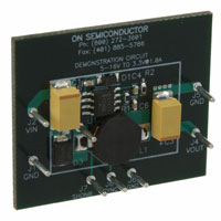
Figure 1. CS51411/3 Demonstration Board
Semiconductor Components Industries, LLC, 2002
January, 2002 – Rev. 1
1
Publication Order Number:
CS51411DEMO/D
�CS51411DEMO/D
ABSOLUTE MAXIMUM RATINGS
Pin Name
Maximum Voltage
Maximum Current
VIN
16 V
2.0 A
VO
16 V
2.0 A
SHDNB
7.0 V
1.0 mA
SYNC
7.0 V
1.0 mA
ELECTRICAL CHARACTERISTICS (TA = 25°C, 5.0 V ≤ VIN ≤ 16 V, 0.1 A ≤ IOUT ≤ 1.0 A, unless otherwise specified.)
Characteristic
Test Conditions
Typ
Unit
–
4.0
%
Output Voltage
Voltage Accuracy
Line Regulation
IOUT = 1.0 A
0.1
%
Load Regulation
VIN = 5.0 V
0.3
%
Minimum Load
–
0.1
A
Transient Response
–
3.0
%
10
µs
–
5.0
ms
–
3.3
V
290 to 470
575 to 900
kHz
kHz
Transient Response Time
Load toggle between 0.1 A and 1.0 A
Startup Time
Input Voltage
Start Threshold
Sync and Shutdown
Sync Frequency
CS51411
CS51413
Minimum Sync Threshold Voltage
–
1.0
V
Minimum Shutdown Threshold Voltage
–
0.3
V
Maximum Shutdown Bias Current
–
12
µA
General
Switching Frequency
CS51411
CS51413
260
520
kHz
kHz
Efficiency
ILOAD = 100 mA
ILOAD = 1.0 A
77.5
83
%
%
100
µA
Shutdown Current
–
http://onsemi.com
2
�CS51411DEMO/D
D1
1N4148
J2
VIN 4–16 V
C2
100 µF
C5
0.1 µF
2
C1
0.1 µF
1
VIN
BOOST
VSW
J1
GND
5
L1
15 µH
3
J3
SWNODE
CS51411/3
SYNC
J4
VOUT 3.3 V
SHDNB
VC
VFB
GND
8
7
6
4
C6
3300 pF
D3
B230DKT_ND
C4
0.1 µF
C3
100 µF
R1
205 Ω
R2
127 Ω
J8
GND
J6
SYNC
J5
GND
J7
SHDNB
Figure 2. Application Diagram
Operation Guidelines
1. Connect input voltage between J2 and J1 on the left
side of the board. The maximum input voltage is
limited by the voltage rating of the input capacitor.
2. Connect the load between J4 and J5. The regulator
requires 100 mA as minimum load. Without this
minimum load, the output may exceed the regulation
voltage.
3. Connect shutdown signal between J7 and J8. When
the voltage on this input is below 0.3 V, the regulator
enters a sleep mode. Pull this input high or leave it
open if not used.
4. The sync signal can be applied between J6 and J8. The
amplitude of the sync pulses needs to be greater than
1.0 V. The duty cycle can vary from 10% to 90%.
Leave it open if not used.
approximately equal to VIN. Now the voltage of the
Boost pin, which connects to C1, is equal to VIN + VO.
Diode D1 is reverse biased. The Boost pin voltage
provides adequate base current to the power transistor,
which lowers VCE(SAT) and improves the energy
transfer efficiency.
2. Soft Start: The soft–start is implemented on the VC pin.
During the startup, the limited source current (25 µA)
of the error amplifier charges the VC pin capacitor. The
rising slope of the VC pin voltage clamps the duty cycle
through the PWM comparator. The VC pin voltage
eventually settles down to a voltage roughly equal to the
reference voltage 1.27 V. Therefore, the startup time can
be easily calculated.
3. Feedback Network: V2 control relies on the output
ripple to provide pulse width modulation. When the
output ripple is inadequate, pulse skipping or
instability may be observed. Adding a capacitor C6 in
parallel with R1 provides a low impedance pass for the
output ripple. Therefore, the output ripple is not
attenuated by the resistor divider. The use of this
capacitor is optional.
Theory Of Operation
1. Boost Strapping Circuit: The boost strapping circuit,
made of C1 and D1, provides a voltage higher than the
input voltage to drive the power transistor (inside IC)
into saturation. The operation of the boost strapping
circuit works as follows. When the power transistor
turns off, diode D3 turns on and pulls the VSW node to
ground. Diode D1 is forward biased, and the output
voltage charges C1 to VO. When the power transistor
turns on, the VSW node is pulled high and is
Please see data sheet for more description on regulator
operation and component selection (document number
CS51411/D available through the Literature Distribution
Center or via our website at http://www.onsemi.com).
http://onsemi.com
3
�CS51411DEMO/D
TYPICAL PERFORMANCE CHARACTERISTICS
3.290
3.300
3.289
3.295
3.287
Output Voltage
Output Voltage
3.288
3.286
3.285
3.284
3.283
3.290
3.285
3.282
3.281
3.280
3.280
5
6
7
8
9
10
11
12
13
14
15
16
0.10 0.20 0.30 0.40 0.50 0.60 0.70 0.80 0.90 1.00
Input Voltage
Output Current
Figure 3. Line Regulation
Figure 4. Load Regulation
88
87
86
Efficiency
85
84
83
82
81
80
79
78
77
0.10 0.20
0.30 0.40 0.50 0.60 0.70 0.80 0.90 1.00
Output Current
Figure 5. Efficiency vs. Output Current
BILL OF MATERIALS
Ref. Designator
Vendor
Part Number
Type
PC/Board
C1, C4, C5
DIGIKEY
PCC1762CT–ND
0.1 µF CERAMIC
3
C2, C3
AVX
TAJE107K016R
100 µF TANTALUM
2
C6
DIGIKEY
PCC1778CT–ND
3300 pF CERAMIC
1
D1
DIGIKEY
LL4148CT–ND
DIODE
1
D3
DIGIKEY
B230DICT–ND
2.0 A SCHOTTKY
1
J1–J8
DIGIKEY
V1055
TEST POINT
8
L1
COILTRONICS
UP2.8B150
15 µH INDUCTOR
1
R1
DIGIKEY
P205CTRND
205 Ω RESISTOR
1
R2
DIGIKEY
P127CTRND
127 Ω RESISTOR
1
U1
ON SEMICONDUCTOR
CS51411/3
CONTROLLER
1
http://onsemi.com
4
�CS51411DEMO/D
DRAWINGS OF LAYERS
Figure 6. Top Copper
Figure 7. Bottom Copper
Figure 8. Top Silk
http://onsemi.com
5
�CS51411DEMO/D
Notes
http://onsemi.com
6
�CS51411DEMO/D
Notes
http://onsemi.com
7
�CS51411DEMO/D
V2 is a trademark of Switch Power, Inc.
ON Semiconductor and
are trademarks of Semiconductor Components Industries, LLC (SCILLC). SCILLC reserves the right to make changes
without further notice to any products herein. SCILLC makes no warranty, representation or guarantee regarding the suitability of its products for any particular
purpose, nor does SCILLC assume any liability arising out of the application or use of any product or circuit, and specifically disclaims any and all liability,
including without limitation special, consequential or incidental damages. “Typical” parameters which may be provided in SCILLC data sheets and/or
specifications can and do vary in different applications and actual performance may vary over time. All operating parameters, including “Typicals” must be
validated for each customer application by customer’s technical experts. SCILLC does not convey any license under its patent rights nor the rights of others.
SCILLC products are not designed, intended, or authorized for use as components in systems intended for surgical implant into the body, or other applications
intended to support or sustain life, or for any other application in which the failure of the SCILLC product could create a situation where personal injury or
death may occur. Should Buyer purchase or use SCILLC products for any such unintended or unauthorized application, Buyer shall indemnify and hold
SCILLC and its officers, employees, subsidiaries, affiliates, and distributors harmless against all claims, costs, damages, and expenses, and reasonable
attorney fees arising out of, directly or indirectly, any claim of personal injury or death associated with such unintended or unauthorized use, even if such claim
alleges that SCILLC was negligent regarding the design or manufacture of the part. SCILLC is an Equal Opportunity/Affirmative Action Employer.
PUBLICATION ORDERING INFORMATION
Literature Fulfillment:
Literature Distribution Center for ON Semiconductor
P.O. Box 5163, Denver, Colorado 80217 USA
Phone: 303–675–2175 or 800–344–3860 Toll Free USA/Canada
Fax: 303–675–2176 or 800–344–3867 Toll Free USA/Canada
Email: ONlit@hibbertco.com
JAPAN: ON Semiconductor, Japan Customer Focus Center
4–32–1 Nishi–Gotanda, Shinagawa–ku, Tokyo, Japan 141–0031
Phone: 81–3–5740–2700
Email: r14525@onsemi.com
ON Semiconductor Website: http://onsemi.com
For additional information, please contact your local
Sales Representative.
N. American Technical Support: 800–282–9855 Toll Free USA/Canada
http://onsemi.com
8
CS51411DEMO/D
�