CS5171BSTEVB
CS5171/3 3.3 V to 5.0 V/
400 mA Boost Regulator
Evaluation Board User's
Manual
http://onsemi.com
EVAL BOARD USER’S MANUAL
Description
Features
• Current Mode Control with Pulse-By-Pulse Current
The CS5171/3 demo board is configured as a compact, low
profile and efficient boost regulator. This board allows initial
evaluation of the performance of the CS5171 (260 kHz) or
the CS5173 (520 kHz) 1.5 A boost regulator IC. The
demonstration circuit converts 3.3 V to 5.0 V with a
maximum load current of 400 mA.
The high integration level of the CS5171 minimizes the
external component count to 10. A high-frequency oscillator
built into CS5171 allows the use of all surface mount
components, greatly reducing the size and height of the
circuit. Using a TTL-compatible pulse train, one can
increase and synchronize the switching frequency to almost
twice the built-in frequency.
This regulator can also be put into a sleep mode. The 5.0 V
output is disabled and the circuit consumes minimum
current. The inherent protection features of the CS5171
ensure that the power supply can survive power-on and
heavy load conditions.
•
•
•
•
•
•
•
•
•
Limit
Easy External Sync Function
Power Down Mode Consuming Maximum 50 mA
Small Board Space Requiring Only 0.7 × 0.7 in.2
Low Profile with Component Height Less Than 0.1 in.
High Energy Transfer Efficiency
Excellent Line and Load Regulation
Fast Transient Response
Minimum Output Voltage Ripple
High Reliability with All Ceramic Capacitors
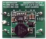
Figure 1. CS5171 Demonstration Board
© Semiconductor Components Industries, LLC, 2012
January, 2012 − Rev. 1
1
Publication Order Number:
EVBUM2054/D
�CS5171BSTEVB
3.3 V
5.0 V
CS5171
Boost
Regulator
SS
GND
GND
Figure 2. Application Diagram
Table 1. ABSOLUTE MAXIMUM RATINGS
Pin Name
Maximum Voltage
Maximum Current
3.3 V
6.3 V
3.0 A
SS
40 V
1.0 mA
5.0 V
6.3 V
400 mA
Stresses exceeding Maximum Ratings may damage the device. Maximum Ratings are stress ratings only. Functional operation above the
Recommended Operating Conditions is not implied. Extended exposure to stresses above the Recommended Operating Conditions may affect
device reliability.
Table 2. ELECTRICAL CHARACTERISTICS (TA = 25°C, VIN = 3.3 V, 60 mA ≤ IOUT ≤ 400 mA; unless otherwise specified.)
Test Conditions
Characteristic
Output Voltage
IOUT = 60 mA
IOUT = 400 mA
Frequency
−
Min
Typ
Max
Units
−
−
4.966
4.963
−
−
V
235
260
290
kHz
Duty Cycle
IOUT = 60 mA
IOUT = 400 mA
−
−
34
48
−
−
%
Efficiency
IOUT = 60 mA
IOUT = 400 mA
−
−
82
78
−
−
%
Line Regulation
3.0 V < VIN < 4.0 V
−
1.5
−
mV/V
Shutdown Current
VC < 0.8 V, VSS = 0 V
−
12
50
mA
Startup Time
From VCC = 1.0 V to IOUT = 400 mA
−
5.6
−
ms
Transient Response Time
From IOUT = 200 mA to IOUT = 400 mA,
VO at Steady State
−
85
−
ms
−
280
−
500
kHz
Sync Range
Sync Pulse Transition Threshold
Rise Time = 20 ns
SS Bias Current
SS = 0 V
SS = 3.3 V
Shutdown Threshold
−
Shutdown Delay
SS = 5.0 V to 0 V, VC < 0.8 V
2.5
−
−
V
−
−
−3.0
3.0
−10
10
mA
0.6
1.3
2.0
V
−
80
300
ms
Table 3. PIN DESCRIPTION
Pin Name
Description
3.3 V
Input voltage pin. Connect this pin to a 3.3 V supply. The maximum voltage rating on this pin is determined by
the rating of the input capacitor.
5.0 V
Output voltage pin. The maximum current drawn from this pin is 400 mA, limited by the inductor. The maximum
voltage rating on this pin is determined by the rating of the output capacitors.
SS
GND
This is a multi-function pin. Apply a TTL pulse train to this pin to sync the switching frequency up to almost twice
the inherent frequency. Pull this pin below 1.2 V to disable the output voltage and leave the board in sleep mode.
Ground pin. There are two ground pins for input and output.
http://onsemi.com
2
�CS5171BSTEVB
R2
1.6 k
1
2
C1
0.01 mF
C2
220 pF
3
4
J1
VC
VSW
FB
PGND
CS5171
NC
AGND
SS
VCC
J4
8
D1
MA10705CT
7
6
L1
22 mH
5
C5
10 mF
C3216X5RJ106M
TP4_220
J2
VIN
3.3 V
R1
4.99 k
R3
560
+5.0 V
C6
10 mF
C3216X5RJ106M
C7
10 mF
C3216X5RJ106M
C4
0.1 mF
PCC1762−ND
J5
J3
GND
GND
Figure 3. Schematic
Operation Guidelines
• The +3.3 V (J2) and GND (J3) input terminals are
located on the left side of the board. Simple alligator or
banana clip connections are needed to power up the
demo board.
• The SS input terminal (J1) is also located on the left
side of the board. Similar connections are required to
input this TTL-compatible logic signal.
• The +5.0 V (J4) and GND (J5) output terminals are
located on the right side of the board. Connect the load
between these two terminals. Never short these
terminals since the IC has no way to protect against a
short in a boost regulator. Place the probe right on the
anode of D1 to examine the output voltage.
• To examine start-up, lift the SS pin above shutdown
threshold. This signal will turn on the IC and enable the
output. The duty cycle and switching frequency are best
observed at the VSW pin.
Theory of Operation
Current Mode Control
The CS5171 incorporates a current mode control scheme,
in which the PWM ramp signal is derived from the power
switch current. This ramp signal is compared to the output
of the error amplifier to control the on-time of the power
switch. The oscillator is only used here as a fixed frequency
clock to ensure a constant operational frequency. At the
beginning of each switching cycle, the clock signal turns on
the internal power switch and the VSW pin voltage is equal
to the saturation voltage of the switch. Since the VSW pin
voltage is applied across the inductor, its current increases
linearly. The current is sensed through an emitter resistor
within the IC. When the current signal reaches the error
amplifier output at the VC pin, the power switch turns off and
inductor current starts to fall. The catch diode D1 is
forward-biased to conduct inductor current. The VSW pin
voltage is now equal to the output voltage plus the diode
forward voltage. Upon the arrival of the next switching
cycle, the power switch turns on again to repeat the same
operation.
This control scheme features several advantages over the
conventional voltage mode controller. First, derived directly
from the inductor, the ramp signal responds immediately to
variations in line voltage, reducing the response time caused
by the output filter and error amplifier delay found in voltage
mode control. The second benefit comes from inherent
pulse-by-pulse current limit by merely clamping the peak
switching current. Finally, since current mode commands an
output current rather than voltage, the filter offers only a
single pole to the feedback loop. This allows both simple
compensation and high bandwidth.
Without discrediting its apparent merits, current mode
control also comes with its own peculiar problems, namely,
subharmonic oscillation at duty cycles over 50%. The
Efficiency (%)
90
80
70
0.01 0.06 0.11 0.16 0.21 0.26 0.31 0.36 0.41 0.46
Current (A)
Figure 4. Efficiency vs. Current
http://onsemi.com
3
�CS5171BSTEVB
switching frequency to a fraction of its nominal value,
reducing the minimum duty cycle, which is otherwise limited
by the minimum on time of the switch. The peak current
during this phase is clamped by the internal current limit.
When the FB pin voltage rises above 0.4 V, the frequency
increases to its nominal value, and the peak current begins
to decrease as the output approaches the regulation voltage.
The overshoot of the output voltage is prevented by the
active pull-on, by which the sink current of the error
amplifier is increased once an overvoltage condition is
detected. The overvoltage condition is defined as when the
FB pin voltage is 50 mV greater than the reference voltage.
CS5171 solves this problem with internal slope
compensation, which adds an artificial ramp to the current
signal. A proper slope is selected to improve circuit stability
without sacrificing the advantages of current mode control.
Short Circuit Condition
When a short circuit condition occurs in a boost circuit,
the IC runs at minimum duty cycle and the diode conducts
for most of the switching period. Since there is no way to
balance the flux of the inductor the inductor current will
eventually saturate, causing excessive current to be drawn
from the input power supply. Since control ICs do not have
the means to limit output current, an external current limit
circuit, such as a fuse or relay, should be added to protect the
IC, inductor and catch diode.
Sync and Shutdown
A TTL-compatible logic input at the S/S pin is capable of
synchronizing the CS5171 up to 500 kHz. As shown in
Figure 6, a rising edge on the SS pin voltage turns on the
power switch, and also resets the oscillator. The duty cycle
of the sync pulse can vary from 10% to 90% without altering
the function. A logic low sustained for typically 80 ms at the
SS pin shuts down the IC and reduces the supply current to
about 30 mA. When the pin is not used, leave it floating.
Start Up
The boost regulator experiences start up transition on
either powering up the VCC pin or pulling up the SS pin. The
difference is that the former generates a high initial current,
which quickly charges the output capacitors to the input
voltage. The start up waveform shown in Figure 5 was
recorded after the 3.3 V input supply was turned on. These
waveforms clearly show the various phases in this power up
transition.
Sync
Current
Ramp
VSW
Figure 6. Timing Diagram of Sync and Shutdown
Design Guidelines
Design Specifications
VIN = 3.3 V ± 10%
VO = 5.0 V ± 5.0%
Maximum Load = 400 mA
Switching Frequency = 260 kHz
Design Output Filter
The resonant frequency of the output filter should be less
than fSW/50, in order to effectively filter out the switching
frequency. The inductor value is selected to keep the current
ripple low according to the equation in Table 4. For the
purposes of this demonstration board, we will select the
maximum ripple current to be 200 mA. Therefore, we
choose an inductor that is 22 mH. Allowing a 5% tolerance
on the output voltage, the maximum output voltage ripple is
25 mV. Using the equation for output voltage ripple and
neglecting the ESR term, the capacitor must be at least 10 mF.
Select the output capacitor to be 20 mF.
The resonant frequency is equal to:
Figure 5. Startup Waveforms
When the VCC voltage is below the minimum supply
voltage, the VSW pin is in high impedance. Therefore,
current conducts directly from the input power source to the
output through the inductor and diode. Once VCC reaches
approximately 1.5 V, the internal power switch briefly turns
on. This is a part of the CS5171’s normal operation. The
turn−on of the power switch accounts for the initial current
swing.
When the VC pin voltage rises above the threshold, the
internal power switch starts to switch and a voltage pulse can
be seen at the VSW pin. Detecting a low output voltage at the
FB pin, the built-in frequency shift feature reduces the
fO +
http://onsemi.com
4
1
+ 7.0 kHz
2p Ǹ(L)(C)
�CS5171BSTEVB
low EMI. The saturation current is 1.1 A and RMS current
rating is 1.0 A.
In a boost converter, the output capacitor sees pulsed
current, which causes significant output ripple on the ESR
of the output capacitor. Ceramic capacitors have the lowest
ESR compared with electrolytic and tantalum capacitors, at
the expense of high cost. Here two 10 mF ceramic capacitors
are used in parallel to double the capacitance. The ESR of
these capacitors is negligible, so the output ripple comes
almost entirely from the charging/discharging of the output
capacitance, as shown in Figure 7. The output ripple is
calculated using the equation in Table 4.
VO(RP) = 48 mV.
Table 4. Formulas for Calculation of Electrical
Parameters in a Boost Regulator
(Assuming Continuous Conduction Mode)
Parameter
Symbol
Formula
Duty Cycle
D
VO ) VF * VIN
VO ) VF * VSAT
Input Current
IIN
ILOAD
1*D
Average Inductor
Current
IL(AVE)
IIN
Inductor Current
Ripple
IL(RP)
VIN * VSAT D
L
fSW
Peak Inductor
Current
IL(PK)
ILOAD(MAX) IL(RP)
)
2
1 * DMAX
Average Switch
Current
ISW(AVE)
ILOAD D
1*D
Peak Switch
Current
ISW(PK)
IL(PK)
Open Switch
Voltage
VSW
VO ) VF
Average Diode
Current
ID(AVE)
ILOAD
Peak Diode
Current
ID(PK)
IL(PK)
VR
VO * VSAT
Diode Reverse
Voltage
Output Ripple
Voltage
VO(RP)
Output Capacitor RMS Current
IC(RMS)
VO * VIN
1
ȡ
VO
fSW COȣ
ILOADȧ V
ȧ
O
Ȣ) VIN ESR
Ȥ
V * VIN
ILOAD Ǹ O
VIN
Figure 7. Output Voltage Ripple and Inductor Current
Select Diode
The diode in a boost converter conducts when the power
switch is turned off. The average diode current is equal to the
load current. The peak reverse voltage of the diode is equal
to the output voltage. Schottky diodes have fast switching
speed and low forward voltage. The diode selected for this
design has a 1.5 A DC current rating and reverse breakdown
voltage of 30 V. An ultra-fast diode is recommended for high
temperature application.
VO = Output Voltage
VIN = Input Voltage
ILOAD = Load Current
CO = Output Capacitance
ESR = Output Capacitor’s Equivalent Series Resistance
fSW = Switching Frequency 260 kHz
VSAT = Power Switch Saturation Voltage (0.6 V typical)
VF = Diode Forward Voltage, 0.5 V for Schottky Diodes and
0.8 V for Ultrafast Recovery Diodes
Compensate the Error Amplifier
Knowing the inductor value, we can calculate the
following parameters using the formulas in Table 4:
DMAX = 50%;
DMIN = 37.4%;
Maximum IIN = 800 mA;
Maximum IL(AVE) = 800 mA;
IL(RP) = 190 mA;
Maximum IL(PK) = 990 mA.
The goal of frequency compensation is to achieve the best
transient response and DC regulation while ensuring the
stability of the system. A typical compensation network, as
shown in Figure 8, provides a two pole, one zero frequency
characteristic. This is further illustrated in the Bode plot
shown in Figure 9.
The DC gain of a transconductance error amplifier can be
calculated as follows:
GainDC + Gm
The inductor’s saturation current rating shall be higher
than IL(PK). If ripple current is small, IL(AVE) is
approximately equal to the RMS current and shall be less
than inductor’s RMS current rating. Coiltronics’ THIN-PAC
inductor is selected for its low profile and its toroidal core for
RO
where:
Gm = error amplifier transconductance;
RO = error amplifier output resistance ≈ 1.0 MΩ.
http://onsemi.com
5
�CS5171BSTEVB
This frequency is low enough to provide over 45_ of phase
lead at 10 kHz to ensure stability. At the same time, the time
constant of C1 × R1 = 51 ms is not too slow to degrade
transient performance. The response of the converter to a
load step can be observed in the “Typical Performance
Characteristics” section in Figure 15.
The low frequency pole, fP1, is determined by the error
amplifier output resistance and C1:
VSW
R1
5.0 k
C2
200 p
CS5171
C1
0.01 m
GND
1
fZ1 +
2pC1R
Figure 8. Typical Compensation Network
DC Gain
O
+ 15 Hz
The second pole, fP2, located in the high frequency range,
can be placed at the output filter’s ESR zero or at half the
switching frequency. Selection of the second pole below the
switching frequency will help to filter out the switching
noises. Here we use 200 pF such that this pole, determined
by C2 and R1, is at:
fP1
fZ1
1
fZ2 +
+ 160 kHz
2pC2R1
fP2
Gain
(dB)
Select Input Capacitors
In boost circuits, the inductor becomes part of the input
filter. In continuous conduction mode, the input current
waveform is triangular and does not contain a large pulsed
current. This reduces the requirements imposed on the input
capacitor selection. The product of this inductor ripple
current and the input capacitor’s ESR determines the VIN
ripple. In this design, a 0.1 mF ceramic cap is used in parallel
with a 10 mF ceramic cap, providing a total capacitance of
10.1 mF. As discussed earlier, the ESR of these capacitors is
negligible, so the VIN ripple is almost entirely due to the
charging and discharging of the capacitors, as shown in
Figure 10.
Frequency (LOG)
Figure 9. Frequency Response of Typical
Compensation Network
A high DC gain is desirable for achieving accurate line and
load regulation. The CS5171 has DC gain of about 60 dB.
The next step is to pick the crossover frequency of the
open loop frequency response. This frequency is typically
set between fSW/10 and fSW/20. We use the 10 kHz as the
crossover frequency in this design. The output capacitors
and load create a pole whose frequency is determined by:
1
fZ1 +
+
2pCRL
2p
1
20 m
12.5
+ 637 Hz
At 10 kHz, this pole generates –31 dB gain on the power
stage. In order to make the loop crossover at 10 kHz, the
error amplifier must provide 31 dB gain. Knowing this, we
can then determine the value of the resistor R1 in Figure 8.
R1 +
31 dB
[ 5.0 k
Gm
C1 and R1 create a zero to provide adequate phase margin
on the crossover frequency. Here we used 0.01 mF capacitor
such that the zero is located at:
1
fZ1 +
+ 3.2 kHz
2pC1R1
Figure 10. Full Load Input Ripple Voltage Waveforms
http://onsemi.com
6
�CS5171BSTEVB
TYPICAL PERFORMANCE CHARACTERISTICS
Figure 11. Full Load Operating Waveforms
Figure 12. Minimum Load Operating Waveforms
Figure 13. Full Load 500 kHz Operating
Waveforms
Figure 14. Minimum Load 500 kHz Operating
Waveforms
Figure 15. Transient Load
http://onsemi.com
7
�CS5171BSTEVB
Table 5. BILL OF MATERIALS
Ref. Des.
Vendor
Part Number
Type
PC/Board
Value
C1
Digikey
PCC1750−ND
Ceramic Cap
1
0.01 mF
C2
Digikey
PCC221ACVCT−ND
Ceramic Cap
1
220 pF
C4
Digikey
PCC1762−ND
Ceramic Cap
1
0.1 mF
C5−C7
TDK
C3216X5RJ106M
Ceramic Cap
3
10 mF
J1
Digikey
5002K−ND
Test Point
1
N/A
N/A
J2−J5
Digikey
V1055
Test Point
4
L1
Coiltronics
TP4_220
Inductor
1
22 mH
R1
Digikey
P4.99KHCT−ND
Resistor
1
4.99 kW
R2
Digikey
P1.6KGCT−ND
Resistor
1
1.6 kW
R3
Digikey
P560GCT−ND
Resistor
1
560 W
D1
Digikey
MA10705CT−ND
Schottky Diode
1
N/A
U1
ON Semiconductor
CS5171/3
Controller
1
N/A
http://onsemi.com
8
�onsemi,
, and other names, marks, and brands are registered and/or common law trademarks of Semiconductor Components Industries, LLC dba “onsemi” or its affiliates
and/or subsidiaries in the United States and/or other countries. onsemi owns the rights to a number of patents, trademarks, copyrights, trade secrets, and other intellectual property. A
listing of onsemi’s product/patent coverage may be accessed at www.onsemi.com/site/pdf/Patent−Marking.pdf. onsemi is an Equal Opportunity/Affirmative Action Employer. This
literature is subject to all applicable copyright laws and is not for resale in any manner.
The evaluation board/kit (research and development board/kit) (hereinafter the “board”) is not a finished product and is not available for sale to consumers. The board is only intended
for research, development, demonstration and evaluation purposes and will only be used in laboratory/development areas by persons with an engineering/technical training and familiar
with the risks associated with handling electrical/mechanical components, systems and subsystems. This person assumes full responsibility/liability for proper and safe handling. Any
other use, resale or redistribution for any other purpose is strictly prohibited.
THE BOARD IS PROVIDED BY ONSEMI TO YOU “AS IS” AND WITHOUT ANY REPRESENTATIONS OR WARRANTIES WHATSOEVER. WITHOUT LIMITING THE FOREGOING,
ONSEMI (AND ITS LICENSORS/SUPPLIERS) HEREBY DISCLAIMS ANY AND ALL REPRESENTATIONS AND WARRANTIES IN RELATION TO THE BOARD, ANY
MODIFICATIONS, OR THIS AGREEMENT, WHETHER EXPRESS, IMPLIED, STATUTORY OR OTHERWISE, INCLUDING WITHOUT LIMITATION ANY AND ALL
REPRESENTATIONS AND WARRANTIES OF MERCHANTABILITY, FITNESS FOR A PARTICULAR PURPOSE, TITLE, NON−INFRINGEMENT, AND THOSE ARISING FROM A
COURSE OF DEALING, TRADE USAGE, TRADE CUSTOM OR TRADE PRACTICE.
onsemi reserves the right to make changes without further notice to any board.
You are responsible for determining whether the board will be suitable for your intended use or application or will achieve your intended results. Prior to using or distributing any systems
that have been evaluated, designed or tested using the board, you agree to test and validate your design to confirm the functionality for your application. Any technical, applications or
design information or advice, quality characterization, reliability data or other services provided by onsemi shall not constitute any representation or warranty by onsemi, and no additional
obligations or liabilities shall arise from onsemi having provided such information or services.
onsemi products including the boards are not designed, intended, or authorized for use in life support systems, or any FDA Class 3 medical devices or medical devices with a similar
or equivalent classification in a foreign jurisdiction, or any devices intended for implantation in the human body. You agree to indemnify, defend and hold harmless onsemi, its directors,
officers, employees, representatives, agents, subsidiaries, affiliates, distributors, and assigns, against any and all liabilities, losses, costs, damages, judgments, and expenses, arising
out of any claim, demand, investigation, lawsuit, regulatory action or cause of action arising out of or associated with any unauthorized use, even if such claim alleges that onsemi was
negligent regarding the design or manufacture of any products and/or the board.
This evaluation board/kit does not fall within the scope of the European Union directives regarding electromagnetic compatibility, restricted substances (RoHS), recycling (WEEE), FCC,
CE or UL, and may not meet the technical requirements of these or other related directives.
FCC WARNING – This evaluation board/kit is intended for use for engineering development, demonstration, or evaluation purposes only and is not considered by onsemi to be a finished
end product fit for general consumer use. It may generate, use, or radiate radio frequency energy and has not been tested for compliance with the limits of computing devices pursuant
to part 15 of FCC rules, which are designed to provide reasonable protection against radio frequency interference. Operation of this equipment may cause interference with radio
communications, in which case the user shall be responsible, at its expense, to take whatever measures may be required to correct this interference.
onsemi does not convey any license under its patent rights nor the rights of others.
LIMITATIONS OF LIABILITY: onsemi shall not be liable for any special, consequential, incidental, indirect or punitive damages, including, but not limited to the costs of requalification,
delay, loss of profits or goodwill, arising out of or in connection with the board, even if onsemi is advised of the possibility of such damages. In no event shall onsemi’s aggregate liability
from any obligation arising out of or in connection with the board, under any theory of liability, exceed the purchase price paid for the board, if any.
The board is provided to you subject to the license and other terms per onsemi’s standard terms and conditions of sale. For more information and documentation, please visit
www.onsemi.com.
PUBLICATION ORDERING INFORMATION
LITERATURE FULFILLMENT:
Email Requests to: orderlit@onsemi.com
onsemi Website: www.onsemi.com
◊
TECHNICAL SUPPORT
North American Technical Support:
Voice Mail: 1 800−282−9855 Toll Free USA/Canada
Phone: 011 421 33 790 2910
www.onsemi.com
1
Europe, Middle East and Africa Technical Support:
Phone: 00421 33 790 2910
For additional information, please contact your local Sales Representative
�