CS8221
Micropower 5.0 V, 100 mA
Low Dropout Linear
Regulator
The CS8221 is a precision 5.0 V, 100 mA micropower voltage
regulator with very low quiescent current (60 mA typical at 100 mA
load). The 5.0 V output is accurate within ±2.0% and supplies 100 mA
of load current with a maximum dropout voltage of only 600 mV.
The regulator is protected against reverse battery, short circuit,
overvoltage, and over temperature conditions. The device can withstand
74 V peak transients making it suitable for use in automotive
environments. The CS8221 is pin for pin compatible with the LM2931.
Features
•
1
12
Low Quiescent Current (60 mA @ 100 mA Load)
5.0 V ±2.0% Output
100 mA Output Current Capability
Internally Fused Leads in SO−8 Package
Fault Protection
− +74 V Peak Transient Voltage
− −15 V Reverse Voltage
− Short Circuit
− Thermal Shutdown
These are Pb−Free Devices
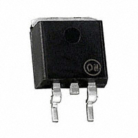
SO−8
DF SUFFIX
CASE 751
8
D2PAK−3
DP SUFFIX
CASE 418AB
3
PIN CONNECTIONS AND
MARKING INDIAGRAM
VOUT
GND
GND
1
SO−8
CS822
ALYW1
G
•
•
•
•
•
http://onsemi.com
NC
8
VIN
GND
GND
NC
D2PAK−3
Tab = GND
CS
Pin 1. VIN
8221
2. GND
AWLYWWG
3. VOUT
1
CS8221 = Specific Device Code
A
= Assembly Location
WL, L = Wafer Lot
Y
= Year
WW, W = Work Week
G or G = Pb−Free Package
ORDERING INFORMATION*
Device
Package
Shipping†
CS8221YDFR8G
SO−8
(Pb−Free)
2500/Tape & Reel
CS8221YDP3G
D2PAK−3
(Pb−Free)
50 Units/Rail
CS8221YDPR3G
D2PAK−3
(Pb−Free)
750/Tape & Reel
*Contact your local sales representative for TO−92
package option.
†For information on tape and reel specifications,
including part orientation and tape sizes, please
refer to our Tape and Reel Packaging Specification
Brochure, BRD8011/D.
© Semiconductor Components Industries, LLC, 2008
October, 2008 − Rev. 9
1
Publication Order Number:
CS8221/D
�CS8221
VOUT
VIN
Current Source
(Circuit Bias)
Over Voltage
Shutdown
Current Limit
Sense
+
−
Error
Amplifier
Thermal
Protection
GND
Bandgap
Reference
Figure 1. Block Diagram
ABSOLUTE MAXIMUM RATINGS*
Rating
Value
Unit
Junction Temperature Range, TJ
−40 to +150
°C
Storage Temperature Range, TSTORAGE
−55 to +150
°C
Internally Limited
−
−15, 74
V
−0.5 to 26
V
Internally Limited
−
2.0
kV
230 peak
°C
Power Dissipation
Peak Transient Voltage (60 V Load Dump @ VIN = 14 V)
Input Operating Range
Output Current
Electrostatic Discharge (Human Body Model)
Lead Temperature Soldering:
Reflow (Note 1)
Stresses exceeding Maximum Ratings may damage the device. Maximum Ratings are stress ratings only. Functional operation above the
Recommended Operating Conditions is not implied. Extended exposure to stresses above the Recommended Operating Conditions may affect
device reliability.
1. 60 seconds maximum above 183°.
*The maximum package power dissipation must be observed.
http://onsemi.com
2
�CS8221
ELECTRICAL CHARACTERISTICS (6.0 ≤ VIN ≤ 26 V, IOUT = 1.0 mA, −40°C ≤ TJ ≤ 125°C unless otherwise noted.)
Characteristic
Test Conditions
Min
Typ
Max
Unit
Output Voltage, VOUT
9.0 V < VIN < 26 V, 100 mA ≤ IOUT ≤ 100 mA
6.0 V ≤ VIN ≤ 26 V, 100 mA ≤ IOUT ≤ 100 mA
4.9
4.85
5.0
5.0
5.1
5.15
V
V
Dropout Voltage (VIN − VOUT)
IOUT = 100 mA
IOUT = 100 mA
−
−
400
100
600
150
mV
mV
Load Regulation
VIN = 14 V, 100 mA ≤ IOUT ≤ 100 mA,
−
5.0
50
mV
Line Regulation
6.0 V < V < 26 V, IOUT = 1.0 mA
−
5.0
50
mV
Quiescent Current, (IQ)
IOUT = 100 mA, VIN = 6.0 V
IOUT = 50 mA
IOUT = 100 mA
−
−
−
60
4.0
12
120
6.0
20
mA
mA
mA
Ripple Rejection
7.0 ≤ VIN ≤ 17 V, IOUT = 100 mA, f = 120 Hz
60
75
−
dB
−
125
200
−
mA
40
125
−
mA
150
180
−
°C
30
34
38
V
Output Stage
Current Limit
Short Circuit Output Current
VOUT = 0 V
Thermal Shutdown (Note 2)
−
Overvoltage Shutdown
VOUT ≤ 1.0 V
2. This parameter is guaranteed by design, but not parametrically tested in production.
PACKAGE LEAD DESCRIPTION
PACKAGE LEAD #
SO−8
D2PAK−3
LEAD SYMBOL
1
3
VOUT
5.0 V, ±2.0%, 100 mA Output.
2, 3, 6, 7
2
GND
Ground.
4
−
NC
No Connection.
5
−
NC
No Connection.
8
1
VIN
Input Voltage.
FUNCTION
TYPICAL PERFORMANCE CHARACTERISTICS
1000
Unstable
Region
CVOUT = 1 mF / 10 mF
100
ESR (W)
Stable Region
10
CVOUT = 1 mF
1
CVOUT = 10 mF
0.1
Unstable Region
0.01
0
10
20
30 40 50 60
70
IOUT OUTPUT CURRENT
80
Figure 2. CS8221 Output Stability
http://onsemi.com
3
90
100
�CS8221
CIRCUIT DESCRIPTION
VOLTAGE REFERENCE AND OUTPUT CIRCUITRY
Should the junction temperature of the power device
exceed 180°C (typ) the power transistor is turned off.
Thermal shutdown is an effective means to prevent die
overheating since the power transistor is the principle heat
source in the IC.
Output Stage Protection
The output stage is protected against overvoltage, short
circuit and thermal runaway conditions (Figure 3).
> 30 V
VOUT
VIN
C1 *
0.1 mF
VIN
VOUT
CS8221
C2**
10 mF
GND
IOUT
Load
Dump
Short
Circuit
*C1 is required if regulator is far from the power source filter.
Thermal
Shutdown
**C2 is required for stability.
Figure 3. Typical Circuit Waveforms for Output
Stage Protection
Figure 4. Application and Test Diagram
If the input voltage rises above 30 V, the output shuts
down. This response protects the internal circuitry and
enables the IC to survive unexpected voltage transients.
APPLICATION NOTES
Step 2: With the input voltage at its maximum value,
increase the load current slowly from zero to full load while
observing the output for any oscillations. If no oscillations
are observed, the capacitor is large enough to ensure a stable
design under steady state conditions.
Step 3: Increase the ESR of the capacitor from zero using
the decade box and vary the load current until oscillations
appear. Record the values of load current and ESR that cause
the greatest oscillation. This represents the worst case load
conditions for the regulator at low temperature.
Step 4: Maintain the worst case load conditions set in
step 3 and vary the input voltage until the oscillations
increase. This point represents the worst case input voltage
conditions.
Step 5: If the capacitor is adequate, repeat steps 3 and 4
with the next smaller valued capacitor. A smaller capacitor
will usually cost less and occupy less board space. If the
output oscillates within the range of expected operating
conditions, repeat steps 3 and 4 with the next larger standard
capacitor value.
Step 6: Test the load transient response by switching in
various loads at several frequencies to simulate its real
working environment. Vary the ESR to reduce ringing.
Step 7: Increase the temperature to your highest operating
temperature. Vary the load current as instructed in step 5 to
test for any oscillations.
STABILITY CONSIDERATIONS
The output or compensation capacitor helps determine
three main characteristics of a linear regulator: start−up
delay, load transient response and loop stability.
The capacitor value and type should be based on cost,
availability, size and temperature constraints. A tantalum or
aluminum electrolytic capacitor is best, since a film or
ceramic capacitor with almost zero ESR can cause
instability. The aluminum electrolytic capacitor is the least
expensive solution, but, if the circuit operates at low
temperatures (−25°C to −40°C), both the value and ESR of
the capacitor will vary considerably. The capacitor
manufacturers data sheet usually provides this information.
The value for the output capacitor COUT shown in Figure
4 should work for most applications, however it is not
necessarily the optimized solution.
To determine an acceptable value for COUT for a particular
application, start with a tantalum capacitor of the
recommended value and work towards a less expensive
alternative part.
Step 1: Place the completed circuit with a tantalum
capacitor of the recommended value in an environmental
chamber at the lowest specified operating temperature and
monitor the outputs with an oscilloscope. A decade box
connected in series with the capacitor will simulate the
higher ESR of an aluminum capacitor. Leave the decade box
outside the chamber, the small resistance added by the
longer leads is negligible.
http://onsemi.com
4
�CS8221
HEAT SINKS
Once the minimum capacitor value with the maximum
ESR is found, a safety factor should be added to allow for the
tolerance of the capacitor and any variations in regulator
performance. Most good quality aluminum electrolytic
capacitors have a tolerance of ± 20% so the minimum value
found should be increased by at least 50% to allow for this
tolerance plus the variation which will occur at low
temperatures. The ESR of the capacitor should be less than
50% of the maximum allowable ESR found in step 3 above.
A heat sink effectively increases the surface area of the
package to improve the flow of heat away from the IC and
into the surrounding air.
Each material in the heat flow path between the IC and the
outside environment will have a thermal resistance. Like
series electrical resistances, these resistances are summed to
determine the value of RΘJA.
RQJA + RQJC ) RQCS ) RQSA
where:
RΘJC = the junction−to−case thermal resistance,
RΘCS = the case−to−heatsink thermal resistance, and
RΘSA = the heatsink−to−ambient thermal resistance.
RΘJC appears in the package section of the data sheet. Like
RΘJA, it too is a function of package type. RΘCS and RΘSA
are functions of the package type, heatsink and the interface
between them. These values appear in heat sink data sheets
of heat sink manufacturers.
CALCULATING POWER DISSIPATION IN A SINGLE
OUTPUT LINEAR REGULATOR
The maximum power dissipation for a single output
regulator (Figure 5) is:
PD(max) + NJVIN(max) * VOUT(min)NjIOUT(max) ) VIN(max)IQ
(1)
where:
VIN(max) is the maximum input voltage,
VOUT(min) is the minimum output voltage,
IOUT(max) is the maximum output current for the
application, and
IQ is the quiescent current the regulator consumes at
IOUT(max).
Once the value of PD(max) is known, the maximum
permissible value of RΘJA can be calculated:
RQJA +
150C * TA
PD
(2)
The value of RΘJA can then be compared with those in the
package section of the data sheet. Those packages with
RΘJA’s less than the calculated value in equation 2 will keep
the die temperature below 150°C.
In some cases, none of the packages will be sufficient to
dissipate the heat generated by the IC, and an external
heatsink will be required.
IIN
IOUT
VIN
(3)
VOUT
CS8221
IQ
Figure 5. Single Output Regulator With Key
Performance Parameters Labeled
SMART REGULATOR is a registered trademark of Semiconductor Components Industries, LLC (SCILLC).
http://onsemi.com
5
�MECHANICAL CASE OUTLINE
PACKAGE DIMENSIONS
D2PAK−3
CASE 418AB
ISSUE B
DATE 18 NOV 2019
A
SCALE 1:1
B
A
E
L1
SEATING
PLANE
0.10
A
B A
NOTES:
1. DIMENSIONING AND TOLERANCING PER ASME
Y14.5M, 1994.
2. CONTROLLING DIMENSION: INCHES.
3. DIMENSIONS D AND E DO NOT INCLUDE MOLD
FLASH AND GATE PROTRUSIONS. MOLD FLASH
AND GATE PROTRUSIONS NOT TO EXCEED
0.005 MAXIMUM PER SIDE. THESE DIMENSIONS
TO BE MEASURED AT DATUM H.
4. THERMAL PAD CONTOUR OPTIONAL WITHIN
DIMENSIONS E, L1, D1, AND E1. DIMENSIONS
D1 AND E1 ESTABLISH A MINIMUM MOUNTING
SURFACE FOR THE THERMAL PAD.
M
E1
c2
E/2
M
D1
D
DETAIL C
H
c
A
e
3X
b
0.13
M
B A
VIEW A−A
B
M
H
SEATING
PLANE
A1
L3
RECOMMENDED
MOUNTING FOOTPRINT*
L
0.424
GAUGE
PLANE
DIM
A
A1
b
c
c2
D
D1
E
E1
e
H
L
L1
L3
M
INCHES
MIN
MAX
0.170
0.180
0.000
0.010
0.026
0.036
0.017
0.026
0.045
0.055
0.325
0.368
0.270
−−−
0.380
0.420
0.245
−−−
0.100 BSC
0.580
0.620
0.090
0.110
−−−
0.066
0.010 BSC
0°
8°
MILLIMETERS
MIN
MAX
4.32
4.57
0.00
0.25
0.66
0.91
0.43
0.66
1.14
1.40
8.25
9.53
6.86
−−−
9.65
10.67
6.22
−−−
2.54 BSC
14.73
15.75
2.29
2.79
−−−
1.68
0.25 BSC
0°
8°
GENERIC
MARKING DIAGRAM*
M
DETAIL C
XX
XXXXXXXXX
AWLYYWWG
0.310
0.631
XXX
A
WL
YY
WW
G
0.180
3X
0.100
PITCH
0.040
DIMENSIONS: MILLIMETERS
*This information is generic. Please refer to
device data sheet for actual part marking.
Pb−Free indicator, “G” or microdot “ G”,
may or may not be present.
*For additional information on our Pb−Free strategy and soldering
details, please download the ON Semiconductor Soldering and
Mounting Techniques Reference Manual, SOLDERRM/D.
DOCUMENT NUMBER:
STATUS:
98AON14121D
ON SEMICONDUCTOR STANDARD
NEW STANDARD:
© Semiconductor Components Industries, LLC, 2002
October, DESCRIPTION:
2002 − Rev. 0
D2PAK−3
= Specific Device Code
= Assembly Location
= Wafer Lot
= Year
= Work Week
= Pb−Free Package
http://onsemi.com
1
Electronic versions are uncontrolled except when
accessed directly from the Document Repository. Printed
versions are uncontrolled except when stamped
“CONTROLLED COPY” in red.
Case Outline Number:
PAGE 1 OFXXX
2
�DOCUMENT NUMBER:
98AON14121D
PAGE 2 OF 2
ISSUE
REVISION
DATE
O
RELEASED FOR PRODUCTION. REQ. BY J. KEISER
18 DEC 2003
A
CHANGES RELATED TO CARSEM TO SEREMBAN TRANSFER. REDREW TO
JEDEC STANDARDS. ADDED SOLDER FOOTPRINT. REQ. BY B. FONTES.
16 SEP 2009
ON Semiconductor and
are registered trademarks of Semiconductor Components Industries, LLC (SCILLC). SCILLC reserves the right to make changes without further notice
to any products herein. SCILLC makes no warranty, representation or guarantee regarding the suitability of its products for any particular purpose, nor does SCILLC assume any liability
arising out of the application or use of any product or circuit, and specifically disclaims any and all liability, including without limitation special, consequential or incidental damages.
“Typical” parameters which may be provided in SCILLC data sheets and/or specifications can and do vary in different applications and actual performance may vary over time. All
operating parameters, including “Typicals” must be validated for each customer application by customer’s technical experts. SCILLC does not convey any license under its patent rights
nor the rights of others. SCILLC products are not designed, intended, or authorized for use as components in systems intended for surgical implant into the body, or other applications
intended to support or sustain life, or for any other application in which the failure of the SCILLC product could create a situation where personal injury or death may occur. Should
Buyer purchase or use SCILLC products for any such unintended or unauthorized application, Buyer shall indemnify and hold SCILLC and its officers, employees, subsidiaries, affiliates,
and distributors harmless against all claims, costs, damages, and expenses, and reasonable attorney fees arising out of, directly or indirectly, any claim of personal injury or death
associated with such unintended or unauthorized use, even if such claim alleges that SCILLC was negligent regarding the design or manufacture of the part. SCILLC is an Equal
Opportunity/Affirmative Action Employer. This literature is subject to all applicable copyright laws and is not for resale in any manner.
© Semiconductor Components Industries, LLC, 2009
September, 2009 − Rev. 01A
Case Outline Number:
418AB
�MECHANICAL CASE OUTLINE
PACKAGE DIMENSIONS
SOIC−8 NB
CASE 751−07
ISSUE AK
8
1
SCALE 1:1
−X−
DATE 16 FEB 2011
NOTES:
1. DIMENSIONING AND TOLERANCING PER
ANSI Y14.5M, 1982.
2. CONTROLLING DIMENSION: MILLIMETER.
3. DIMENSION A AND B DO NOT INCLUDE
MOLD PROTRUSION.
4. MAXIMUM MOLD PROTRUSION 0.15 (0.006)
PER SIDE.
5. DIMENSION D DOES NOT INCLUDE DAMBAR
PROTRUSION. ALLOWABLE DAMBAR
PROTRUSION SHALL BE 0.127 (0.005) TOTAL
IN EXCESS OF THE D DIMENSION AT
MAXIMUM MATERIAL CONDITION.
6. 751−01 THRU 751−06 ARE OBSOLETE. NEW
STANDARD IS 751−07.
A
8
5
S
B
0.25 (0.010)
M
Y
M
1
4
−Y−
K
G
C
N
X 45 _
SEATING
PLANE
−Z−
0.10 (0.004)
H
M
D
0.25 (0.010)
M
Z Y
S
X
J
S
8
8
1
1
IC
4.0
0.155
XXXXX
A
L
Y
W
G
IC
(Pb−Free)
= Specific Device Code
= Assembly Location
= Wafer Lot
= Year
= Work Week
= Pb−Free Package
XXXXXX
AYWW
1
1
Discrete
XXXXXX
AYWW
G
Discrete
(Pb−Free)
XXXXXX = Specific Device Code
A
= Assembly Location
Y
= Year
WW
= Work Week
G
= Pb−Free Package
*This information is generic. Please refer to
device data sheet for actual part marking.
Pb−Free indicator, “G” or microdot “G”, may
or may not be present. Some products may
not follow the Generic Marking.
1.270
0.050
SCALE 6:1
INCHES
MIN
MAX
0.189
0.197
0.150
0.157
0.053
0.069
0.013
0.020
0.050 BSC
0.004
0.010
0.007
0.010
0.016
0.050
0 _
8 _
0.010
0.020
0.228
0.244
8
8
XXXXX
ALYWX
G
XXXXX
ALYWX
1.52
0.060
0.6
0.024
MILLIMETERS
MIN
MAX
4.80
5.00
3.80
4.00
1.35
1.75
0.33
0.51
1.27 BSC
0.10
0.25
0.19
0.25
0.40
1.27
0_
8_
0.25
0.50
5.80
6.20
GENERIC
MARKING DIAGRAM*
SOLDERING FOOTPRINT*
7.0
0.275
DIM
A
B
C
D
G
H
J
K
M
N
S
mm Ǔ
ǒinches
*For additional information on our Pb−Free strategy and soldering
details, please download the ON Semiconductor Soldering and
Mounting Techniques Reference Manual, SOLDERRM/D.
STYLES ON PAGE 2
DOCUMENT NUMBER:
DESCRIPTION:
98ASB42564B
SOIC−8 NB
Electronic versions are uncontrolled except when accessed directly from the Document Repository.
Printed versions are uncontrolled except when stamped “CONTROLLED COPY” in red.
PAGE 1 OF 2
onsemi and
are trademarks of Semiconductor Components Industries, LLC dba onsemi or its subsidiaries in the United States and/or other countries. onsemi reserves
the right to make changes without further notice to any products herein. onsemi makes no warranty, representation or guarantee regarding the suitability of its products for any particular
purpose, nor does onsemi assume any liability arising out of the application or use of any product or circuit, and specifically disclaims any and all liability, including without limitation
special, consequential or incidental damages. onsemi does not convey any license under its patent rights nor the rights of others.
© Semiconductor Components Industries, LLC, 2019
www.onsemi.com
�SOIC−8 NB
CASE 751−07
ISSUE AK
DATE 16 FEB 2011
STYLE 1:
PIN 1. EMITTER
2. COLLECTOR
3. COLLECTOR
4. EMITTER
5. EMITTER
6. BASE
7. BASE
8. EMITTER
STYLE 2:
PIN 1. COLLECTOR, DIE, #1
2. COLLECTOR, #1
3. COLLECTOR, #2
4. COLLECTOR, #2
5. BASE, #2
6. EMITTER, #2
7. BASE, #1
8. EMITTER, #1
STYLE 3:
PIN 1. DRAIN, DIE #1
2. DRAIN, #1
3. DRAIN, #2
4. DRAIN, #2
5. GATE, #2
6. SOURCE, #2
7. GATE, #1
8. SOURCE, #1
STYLE 4:
PIN 1. ANODE
2. ANODE
3. ANODE
4. ANODE
5. ANODE
6. ANODE
7. ANODE
8. COMMON CATHODE
STYLE 5:
PIN 1. DRAIN
2. DRAIN
3. DRAIN
4. DRAIN
5. GATE
6. GATE
7. SOURCE
8. SOURCE
STYLE 6:
PIN 1. SOURCE
2. DRAIN
3. DRAIN
4. SOURCE
5. SOURCE
6. GATE
7. GATE
8. SOURCE
STYLE 7:
PIN 1. INPUT
2. EXTERNAL BYPASS
3. THIRD STAGE SOURCE
4. GROUND
5. DRAIN
6. GATE 3
7. SECOND STAGE Vd
8. FIRST STAGE Vd
STYLE 8:
PIN 1. COLLECTOR, DIE #1
2. BASE, #1
3. BASE, #2
4. COLLECTOR, #2
5. COLLECTOR, #2
6. EMITTER, #2
7. EMITTER, #1
8. COLLECTOR, #1
STYLE 9:
PIN 1. EMITTER, COMMON
2. COLLECTOR, DIE #1
3. COLLECTOR, DIE #2
4. EMITTER, COMMON
5. EMITTER, COMMON
6. BASE, DIE #2
7. BASE, DIE #1
8. EMITTER, COMMON
STYLE 10:
PIN 1. GROUND
2. BIAS 1
3. OUTPUT
4. GROUND
5. GROUND
6. BIAS 2
7. INPUT
8. GROUND
STYLE 11:
PIN 1. SOURCE 1
2. GATE 1
3. SOURCE 2
4. GATE 2
5. DRAIN 2
6. DRAIN 2
7. DRAIN 1
8. DRAIN 1
STYLE 12:
PIN 1. SOURCE
2. SOURCE
3. SOURCE
4. GATE
5. DRAIN
6. DRAIN
7. DRAIN
8. DRAIN
STYLE 13:
PIN 1. N.C.
2. SOURCE
3. SOURCE
4. GATE
5. DRAIN
6. DRAIN
7. DRAIN
8. DRAIN
STYLE 14:
PIN 1. N−SOURCE
2. N−GATE
3. P−SOURCE
4. P−GATE
5. P−DRAIN
6. P−DRAIN
7. N−DRAIN
8. N−DRAIN
STYLE 15:
PIN 1. ANODE 1
2. ANODE 1
3. ANODE 1
4. ANODE 1
5. CATHODE, COMMON
6. CATHODE, COMMON
7. CATHODE, COMMON
8. CATHODE, COMMON
STYLE 16:
PIN 1. EMITTER, DIE #1
2. BASE, DIE #1
3. EMITTER, DIE #2
4. BASE, DIE #2
5. COLLECTOR, DIE #2
6. COLLECTOR, DIE #2
7. COLLECTOR, DIE #1
8. COLLECTOR, DIE #1
STYLE 17:
PIN 1. VCC
2. V2OUT
3. V1OUT
4. TXE
5. RXE
6. VEE
7. GND
8. ACC
STYLE 18:
PIN 1. ANODE
2. ANODE
3. SOURCE
4. GATE
5. DRAIN
6. DRAIN
7. CATHODE
8. CATHODE
STYLE 19:
PIN 1. SOURCE 1
2. GATE 1
3. SOURCE 2
4. GATE 2
5. DRAIN 2
6. MIRROR 2
7. DRAIN 1
8. MIRROR 1
STYLE 20:
PIN 1. SOURCE (N)
2. GATE (N)
3. SOURCE (P)
4. GATE (P)
5. DRAIN
6. DRAIN
7. DRAIN
8. DRAIN
STYLE 21:
PIN 1. CATHODE 1
2. CATHODE 2
3. CATHODE 3
4. CATHODE 4
5. CATHODE 5
6. COMMON ANODE
7. COMMON ANODE
8. CATHODE 6
STYLE 22:
PIN 1. I/O LINE 1
2. COMMON CATHODE/VCC
3. COMMON CATHODE/VCC
4. I/O LINE 3
5. COMMON ANODE/GND
6. I/O LINE 4
7. I/O LINE 5
8. COMMON ANODE/GND
STYLE 23:
PIN 1. LINE 1 IN
2. COMMON ANODE/GND
3. COMMON ANODE/GND
4. LINE 2 IN
5. LINE 2 OUT
6. COMMON ANODE/GND
7. COMMON ANODE/GND
8. LINE 1 OUT
STYLE 24:
PIN 1. BASE
2. EMITTER
3. COLLECTOR/ANODE
4. COLLECTOR/ANODE
5. CATHODE
6. CATHODE
7. COLLECTOR/ANODE
8. COLLECTOR/ANODE
STYLE 25:
PIN 1. VIN
2. N/C
3. REXT
4. GND
5. IOUT
6. IOUT
7. IOUT
8. IOUT
STYLE 26:
PIN 1. GND
2. dv/dt
3. ENABLE
4. ILIMIT
5. SOURCE
6. SOURCE
7. SOURCE
8. VCC
STYLE 29:
PIN 1. BASE, DIE #1
2. EMITTER, #1
3. BASE, #2
4. EMITTER, #2
5. COLLECTOR, #2
6. COLLECTOR, #2
7. COLLECTOR, #1
8. COLLECTOR, #1
STYLE 30:
PIN 1. DRAIN 1
2. DRAIN 1
3. GATE 2
4. SOURCE 2
5. SOURCE 1/DRAIN 2
6. SOURCE 1/DRAIN 2
7. SOURCE 1/DRAIN 2
8. GATE 1
DOCUMENT NUMBER:
DESCRIPTION:
98ASB42564B
SOIC−8 NB
STYLE 27:
PIN 1. ILIMIT
2. OVLO
3. UVLO
4. INPUT+
5. SOURCE
6. SOURCE
7. SOURCE
8. DRAIN
STYLE 28:
PIN 1. SW_TO_GND
2. DASIC_OFF
3. DASIC_SW_DET
4. GND
5. V_MON
6. VBULK
7. VBULK
8. VIN
Electronic versions are uncontrolled except when accessed directly from the Document Repository.
Printed versions are uncontrolled except when stamped “CONTROLLED COPY” in red.
PAGE 2 OF 2
onsemi and
are trademarks of Semiconductor Components Industries, LLC dba onsemi or its subsidiaries in the United States and/or other countries. onsemi reserves
the right to make changes without further notice to any products herein. onsemi makes no warranty, representation or guarantee regarding the suitability of its products for any particular
purpose, nor does onsemi assume any liability arising out of the application or use of any product or circuit, and specifically disclaims any and all liability, including without limitation
special, consequential or incidental damages. onsemi does not convey any license under its patent rights nor the rights of others.
© Semiconductor Components Industries, LLC, 2019
www.onsemi.com
�onsemi,
, and other names, marks, and brands are registered and/or common law trademarks of Semiconductor Components Industries, LLC dba “onsemi” or its affiliates
and/or subsidiaries in the United States and/or other countries. onsemi owns the rights to a number of patents, trademarks, copyrights, trade secrets, and other intellectual property.
A listing of onsemi’s product/patent coverage may be accessed at www.onsemi.com/site/pdf/Patent−Marking.pdf. onsemi reserves the right to make changes at any time to any
products or information herein, without notice. The information herein is provided “as−is” and onsemi makes no warranty, representation or guarantee regarding the accuracy of the
information, product features, availability, functionality, or suitability of its products for any particular purpose, nor does onsemi assume any liability arising out of the application or use
of any product or circuit, and specifically disclaims any and all liability, including without limitation special, consequential or incidental damages. Buyer is responsible for its products
and applications using onsemi products, including compliance with all laws, regulations and safety requirements or standards, regardless of any support or applications information
provided by onsemi. “Typical” parameters which may be provided in onsemi data sheets and/or specifications can and do vary in different applications and actual performance may
vary over time. All operating parameters, including “Typicals” must be validated for each customer application by customer’s technical experts. onsemi does not convey any license
under any of its intellectual property rights nor the rights of others. onsemi products are not designed, intended, or authorized for use as a critical component in life support systems
or any FDA Class 3 medical devices or medical devices with a same or similar classification in a foreign jurisdiction or any devices intended for implantation in the human body. Should
Buyer purchase or use onsemi products for any such unintended or unauthorized application, Buyer shall indemnify and hold onsemi and its officers, employees, subsidiaries, affiliates,
and distributors harmless against all claims, costs, damages, and expenses, and reasonable attorney fees arising out of, directly or indirectly, any claim of personal injury or death
associated with such unintended or unauthorized use, even if such claim alleges that onsemi was negligent regarding the design or manufacture of the part. onsemi is an Equal
Opportunity/Affirmative Action Employer. This literature is subject to all applicable copyright laws and is not for resale in any manner.
PUBLICATION ORDERING INFORMATION
LITERATURE FULFILLMENT:
Email Requests to: orderlit@onsemi.com
onsemi Website: www.onsemi.com
◊
TECHNICAL SUPPORT
North American Technical Support:
Voice Mail: 1 800−282−9855 Toll Free USA/Canada
Phone: 011 421 33 790 2910
Europe, Middle East and Africa Technical Support:
Phone: 00421 33 790 2910
For additional information, please contact your local Sales Representative
�


 工商网监
湘ICP备2023018690号
工商网监
湘ICP备2023018690号