CS8371 8.0 V/1.0 A, 5.0 V/250 mA Dual Regulator with Independent Output Enables and NOCAPt
The CS8371 is an 8.0 V/5.0 V dual output linear regulator. The 8.0 V ±5.0% output sources 1.0 A, while the 5.0 V ±5.0% output sources 250 mA. Each output is controlled by its own ENABLE lead. Setting the ENABLE input high turns on the associated regulator output. Holding both ENABLE inputs low puts the IC into sleep mode where current consumption is less than 10 mA. The regulator is protected against overvoltage, short−circuit and thermal runaway conditions. The device can withstand 45 V load dump transients making suitable for use in automotive environments. ON’s proprietary NOCAP solution is the first technology which allows the output to be stable without the use of an external capacitor. The CS8371 is available in a 7 lead TO−220 package with copper tab. The tab can be connected to a heatsink if necessary.
Features http://onsemi.com
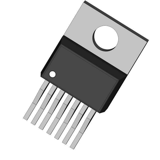
TO−220 SEVEN LEAD T SUFFIX CASE 821E
1 7
1
TO−220 SEVEN LEAD TVA SUFFIX CASE 821J
PIN CONNECTIONS AND MARKING DIAGRAM
Tab = GND Pin 1. ENABLE1 2. ENABLE2 3. VOUT2 4. GND 5. Sense 6. VCC 7. VOUT1
• Two Regulated Outputs − 8.0 V ±5.0%; 1.0 A − 5.0 V ±5.0%; 250 mA • Independent ENABLE for Each Output • Seperate Sense Feedback Lead for 8.0 V Output • < 10 mA Sleep Mode Current • Fault Protection − Overvoltage Shutdown − +45 V Peak Transient Voltage − Short Circuit − Thermal Shutdown • CMOS Compatible, Low Current ENABLE Inputs • Pb−Free Packages are Available*
CS 8371 AWLYWWG
CS 8371 AWLYWWG
A WL Y WW G
= Assembly Location = Wafer Lot = Year = Work Week = Pb−Free Package
ORDERING INFORMATION
Device CS8371ET7 CS8371ET7G Package TO−220 STRAIGHT TO−220 STRAIGHT (Pb−Free) TO−220 VERTICAL TO−220 VERTICAL (Pb−Free) Shipping 50 Units/Rail 50 Units/Rail
CS8371ETVA7 CS8371ETVA7G
50 Units/Rail 50 Units/Rail
*For additional information on our Pb−Free strategy and soldering details, please download the ON Semiconductor Soldering and Mounting Techniques Reference Manual, SOLDERRM/D.
© Semiconductor Components Industries, LLC, 2006
1
June, 2006 − Rev. 12
Publication Order Number: CS8371/D
�CS8371
VCC
Overvoltage Shutdown
VOUT1
Current Limit
ENABLE1
− +
1.2 V
Pre−Regulator Bias Generator
+ −
Sense
NOCAP
Trimmed Bandgap Voltage Reference
Thermal Shutdown
ENABLE2
− +
1.2 V
− +
VOUT2
Current Limit
GND
Figure 1. Block Diagram
MAXIMUM RATINGS
Rating Power Dissipation ENABLE Input Voltage Range Load Current (8.0 V Regulator) Load Current (5.0 V Regulator) Transient Peak Voltage (31 V Load Dump @ 14 V VCC) Storage Temperature Range Junction Temperature Range Lead Temperature Soldering: Wave Solder (through hole styles only) (Note 1) Value Internally Limited −0.6 to +10 Internally Limited Internally Limited 45 −65 to +150 −40 to +150 260 peak Unit − V − − V °C °C °C
Stresses exceeding Maximum Ratings may damage the device. Maximum Ratings are stress ratings only. Functional operation above the Recommended Operating Conditions is not implied. Extended exposure to stresses above the Recommended Operating Conditions may affect device reliability. 1. 10 second maximum.
http://onsemi.com
2
�CS8371
ELECTRICAL CHARACTERISTICS: (−40°C ≤ TA ≤ +85°C, 10.5 V ≤ VCC ≤ 16 V, ENABLE1 = ENABLE2 = 5.0 V, IOUT1 = IOUT2 = 5.0 mA, unless otherwise stated.)
Characteristic PRIMARY OUTPUT (VOUT1) Output Voltage Line Regulation Load Regulation Sleep Mode Quiescent Current Quiescent Current Dropout Voltage Quiescent Bias Current IOUT1 = 1.0 A 10.5 V ≤ VCC ≤ 26 V 5.0 mA ≤ IOUT1 ≤ 1.0 A VCC = 14 V, ENABLE1 = ENABLE2 = 0 V VCC = 14 V, IOUT1 = 1.0 A, IOUT2 = 250 mA IOUT1 = 250 mA IOUT1 = 1.0 A IOUT1 = 5.0 mA, ENABLE2 = 0 V, VCC = 14 V, IQ = ICC − IOUT1 IOUT1 = 1.0 A, ENABLE2 = 0 V, VCC = 14 V, IQ = ICC − IOUT1 f = 120 Hz, VCC = 14 V with 1.0 VPP AC, COUT = 0 mF f = 10 kHz, VCC = 14 V with 1.0 VPP AC, COUT = 0 mF f = 20 kHz, VCC = 14 V with 1.0 VPP AC, COUT = 0 mF VCC = 16 V 5.0 mA ≤ IREG1 ≤ 1.0 A 10 Hz − 100 kHz 7.60 − − 0 − − − − 8.00 − − 0.2 − − − − − 8.40 50 150 10.0 30 1.2 1.5 10 22 V mV mV mA mA V V mA mA Test Conditions Min Typ Max Unit
Ripple Rejection
− − − 1.1 − −
90 74 68 − − 300
− − − 2.5 6.0 −
dB dB dB A V mVrms
Current Limit Overshoot Voltage Output Noise SECONDARY OUTPUT (VOUT2) Output Voltage Line Regulation Load Regulation Dropout Voltage Quiescent Bias Current
IOUT2 = 250 mA 7.0 V ≤ VCC ≤ 26 V 5.0 mA ≤ IOUT2 ≤ 250 mA IOUT2 = 5.0 mA IOUT2 = 250 mA IOUT2 = 5.0 mA, ENABLE1 = 0 V, VCC = 14 V, IQ = ICC − IOUT2 IOUT2 = 250 mA, ENABLE1 = 0 V, VCC = 14 V, IQ = ICC − IOUT2 f = 120 Hz, VCC = 14 V with 1.0 VPP AC, COUT = 0 mF f = 10 kHz, VCC = 14 V with 1.0 VPP AC, COUT = 0 mF f = 20 kHz, VCC = 14 V with 1.0 VPP AC, COUT = 0 mF VCC = 16 V 5.0 mA ≤ IREG2 ≤ 250 mA 10 Hz − 100 kHz
4.75 − − − − −
5.00 − − − − − −
5.25 40 100 2.2 2.5 7.0 8.0
V mV mV V V mA mA
Ripple Rejection
− − − 270 − −
90 75 67 − − 170
− − − 600 4.3 −
dB dB dB mA V mVrms
Current Limit Overshoot Voltage Output Noise ENABLE FUNCTION (ENABLE) Input Current Input Voltage PROTECTION CIRCUITRY ESD Threshold Overvoltage Shutdown Thermal Shutdown Thermal Hysteresis
VCC = 14 V, 0 V ≤ ENABLE ≤ 5.5 V Low High
−150 0 2.0
− − −
150 0.8 5.0
mA V V
Human Body Model − Guaranteed by Design −
±2.0 24 150 −
±4.0 − 180 30
− 30 − −
kV V °C °C
http://onsemi.com
3
�CS8371
PACKAGE PIN DESCRIPTION
PACKAGE LEAD # 7 Lead TO−220 1 2 3 4 5 6 7 LEAD SYMBOL ENABLE1 ENABLE2 VOUT2 GND Sense VCC VOUT1 FUNCTION ENABLE control for the 8.0 V, 1.0 A output. ENABLE control for the 5.0 V, 250 mA output. 5.0 V ±5.0%, 250 mA regulated output. Ground. Sense feedback for the primary 8.0 V output. Supply voltage, usually from battery. 8.0 V ±5.0%, 1.0 A regulated output.
TYPICAL PERFORMANCE CHARACTERISTICS
8.05 8.04 8.03 Output Voltage (V) 8.02 8.01 8.00 7.99 7.98 7.97 7.96 7.95
−40 −20 0 20 40 60 80 100 120 140 VIN = 14 V IOUT = 1.0 A
5.00
Output Voltage (V)
4.95
VIN = 14 V IOUT = 250 mA
4.90
4.85
−40 −20 0 20 40 60 80 100 120 140
Ambient Temperature (°C)
Ambient Temperature (°C)
Figure 2. Regulator 1 Output Voltage
2.0 1.8 1.6 Dropout Voltage (V) 1.4 1.2 1.0 0.8 0.6 0.4 0.2 0
0 100 200 300 400 500 600 700 800 900 1000 25°C −40°C 85°C
Figure 3. Regulator 2 Output Voltage
2.5
2.0 Dropout Voltage (V)
−40°C
1.5
25°C
85°C
1.0
0.5
0
0 50 100 150 200 250
Output Current (mA)
Output Current (mA)
Figure 4. Regulator 1 Dropout Voltage
Figure 5. Regulator 2 Dropout Voltage
http://onsemi.com
4
�CS8371
TYPICAL PERFORMANCE CHARACTERISTICS
10 9 Reg 1 Output Voltage (V) 8 7 6 5 4 3 2 1 0
0 1 2 3 VIN = 14 V TA = 25°C
10 9 Reg 2 Output Voltage (V) 8 7 6 5 4 3 2 1 0
0 100 200 300 400 500 VIN = 14 V TA = 25°C
Reg 1 Output Current (A)
Reg 2 Output Current (mA)
Figure 6. Regulator 1 Current Limit
9.0 8.5 Quiescent Current (mA0 8.0 7.5 7.0 6.5 6.0 5.5 5.0 4.5 4.0
−40 −20 0 20 40 60 80 Enable 1 = 5.0 V Enable 2 = 5.0 V VIN = 14 V IOUT1 = 1.0 A IOUT2 = 250 mA
Figure 7. Regulator 2 Current Limit
1.0 0.9 Quiescent Current (mA) 0.8 0.7 0.6 0.5 0.4 0.3 0.2 0.1 0
−40 −20 0 20 40 60 80 Enable 1 = 0 V Enable 2 = 0 V VIN = 14 V
Ambient Temperature (°C)
Ambient Temperature (°C)
Figure 8. Quiescent Current
6.0 5.5 Quiescent Current (mA) 5.0 4.5
IOUT = 5.0 mA IOUT = 1.0 A Enable 1 = 5.0 V Enable 2 = 0 V VIN = 14 V
Figure 9. Quiescent Current
4.0 3.8 Quiescent Current (mA) 3.6 3.4 3.2 3.0 2.8 2.6 2.4 2.2
IOUT = 5.0 mA IOUT = 250 mA Enable 1 = 0 V Enable 2 = 5.0 V VIN = 14 V
4.0 3.5 3.0
−40
−20
0
20
40
60
80
2.0
−40
−20
0
20
40
60
80
Ambient Temperature (°C)
Ambient Temperature (°C)
Figure 10. Regulator 1 Quiescent Current
Figure 11. Regulator 2 Quiescent Current
http://onsemi.com
5
�CS8371
TYPICAL PERFORMANCE CHARACTERISTICS
8.020
VIN = 14 V
5.02
VIN = 14 V
8.015 Output Voltage (V) Output Voltage (V) 8.010 8.005 8.000 7.995 7.990 7.985 7.980
0 100 200 300 400 500 600 700 800 900 1000 25°C −40°C 85°C
5.01 5.00 4.99 4.98 4.97 4.96 4.95 4.94
0 50 100 150 200 250 −40°C 85°C 25°C
Output Current (mA)
Output Current (mA)
Figure 12. Regulator 1 Load Regulation
Figure 13. Regulator 2 Load Regulation
Reg 1 Output Voltage (V)
8 7 6 5 4 3 2 1 0 5 4 3 2 1 0
0
Reg 2 Output Voltage (V)
COUT = 0 mF TA = 25°C IOUT = 5.0 mA
8 7 6 5 4 3 2 1 0 5 4 3 2 1 0
0
COUT = 0 mF TA = 25°C IOUT = 5.0 mA
Enable 1 (V)
1
2
3
4
5
6
7
8
9
10
11
12
Enable 2 (V)
1
2
3
4
5
6
7
8
9
10
11
12
Time (ms)
Time (ms)
Figure 14. Regulator 1 Startup
Input Voltage (V) Output Voltage Deviation (V) Input Voltage (V) Output Voltage Deviation (V)
Figure 15. Regulator 2 Startup
2 1 0 −1 −2
COUT = 0 mF TA = 25°C
0.6 0.4 0.2 0 −0.2 −0.4 −0.6
COUT = 0 mF TA = 25°C
16 14 12 10
0 100 200 300 400 500 600
16 14 12 10
0 100 200 300 400 500 600
Time (ns)
Time (ns)
Figure 16. Regulator 1 Line Transient Response
Figure 17. Regulator 2 Line Transient Response
http://onsemi.com
6
�CS8371
TYPICAL PERFORMANCE CHARACTERISTICS
Load Current (mA) Output Voltage Deviation (mV) Load Current (mA) Output Voltage Deviation (V)
3 2 1 0 −1 −2 −3
VIN = 14 V COUT = 0 mF TA = 25°C
+500
VIN = 14 V COUT = 0 mF TA = 25°C
0
−500
1000 5
0 5 10 15 20 25 30
250 5
0 5 10 15 20 25 30
Time (ms)
Time (ms)
Figure 18. Regulator 1 Load Transient Response
Figure 19. Regulator 2 Load Transient Response
100 Ripple Rejection (dB)
TA = 25°C VIN = 14 V COUT = 0 mF
100 Ripple Rejection (dB)
TA = 25°C VIN = 14 V COUT = 0 mF
80
80
60
60
40
40
20
1 10 100 1k 10k 100k 1M
20
1 10 100 1k 10k 100k 1M
Frequency (Hz)
Frequency (Hz)
Figure 20. Regulator 1 Ripple Rejection
Figure 21. Regulator 2 Ripple Rejection
5 Output Capacitor ESR (W)
TA = 25°C VIN = 14 V RESR ≤ 1.6 W IOUT = 5.0 mA to 1.0 A
1
Unstable Region
0
.01 0.1 1 10 100 1000
Output Capacitor Size (mF)
Figure 22. Regulator 1 Stability
http://onsemi.com
7
�CS8371
DEFINITION OF TERMS Dropout Voltage − The input−output voltage differential at which the circuit ceases to regulate against further reduction in input voltage. Measured when the output voltage has dropped 100 mV from the nominal value obtained at 14 V input, dropout voltage is dependent upon load current and junction temperature. Current Limit − Peak current that can be delivered to the output. Input Voltage − The DC voltage applied to the input terminals with respect to ground. Input Output Differential − The voltage difference between the unregulated input voltage and the regulated output voltage for which the regulator will operate. Line Regulation − The change in output voltage for a change in the input voltage. The measurement is made under conditions of low dissipation or by using pulse techniques such that the average chip temperature is not significantly affected. Load Regulation − The change in output voltage for a change in load current at constant chip temperature. Long Term Stability − Output voltage stability under accelerated life−test conditions after 1000 hours with maximum rated voltage and junction temperature. Output Noise Voltage − The rms AC voltage at the output, with constant load and no input ripple, measured over a specified frequency range. Quiescent Current − The part of the positive input current that does not contribute to the positive load current. The regulator ground lead current. Ripple Rejection − The ratio of the peak−to−peak input ripple voltage to the peak−to−peak output ripple voltage. Temperature Stability of VOUT − The percentage change in output voltage for a thermal variation from room temperature to either temperature extreme.
C1* 0.1 mF
VIN
VOUT1
8.0 V
Control
ENABLE1 ENABLE2
CS8371
5.0 V VOUT2 GND
Tuner IC
* C1 is required if the regulator is far from the power source filter.
Figure 23. Applications Circuit
APPLICATION NOTES With seperate control of each output channel, the CS8371 is ideal for applications where each load must be switched independently. In an automotive radio, the 8.0 V output drives the displays and tape drive motors while the 5.0 V output supplies the Tuner IC and memory.
Stability Considerations/NOCAP
Normally a low dropout or quasi−low dropout regulator (or any type requiring a slow lateral PNP in the control loop) necessitates a large external compensation capacitor at the output of the IC. The external capacitor is also used to curtail overshoot, determine startup delay time and load transient response. Traditional LDO regulators typically have low unity gain bandwidth, display overshoot and poor ripple rejection. Compensation is also an issue because the high frequency
load capacitor value, ESR (Equivalent Series Resistance) and board layout parasitics all can create oscillations if not properly accounted for. NOCAP is an ON Semiconductor exclusive output stage which internally compensates the LDO regulator over temperature, load and line variations without the need for an expensive external capacitor. It incorporates high gain (>80 dB) and large unity gain bandwidth (>100 kHz) while maintaining many of the characteristics of a single−pole amplifier (large phase margin and no overshoot). NOCAP is ideally suited for slow switching or steady loads. If the load displays large transient current requirements, such as with high frequency microprocessors, an output storage capacitor may be needed. Some large capacitor and small capacitor ESR values at the output may
http://onsemi.com
8
�CS8371
cause small signal oscillations at the output. This will depend on the load conditions. With these types of loads, a traditional output stage may be better suited for proper operation. Output 1 employs NOCAP. Refer to the plots in the Typical Performance Characteristics section for appropriate output capacitor selections for stability if an external capacitor is required by the switching characteristics of the load. Output 2 has a Darlington NPN−type output structure and is inherently stable with any type of capacitive load or no capacitor at all.
Calculating Power Dissipation in a Dual Output Linear Regulator
In some cases, none of the packages will be sufficient to dissipate the heat generated by the IC, and an external heatsink will be required.
IIN VIN IOUT1 VOUT1
SMART REGULATOR®
Control Features
IOUT2 VOUT2
IQ
The maximum power dissipation for a dual output regulator (Figure 24) is
PD(max) + VIN(max) * VOUT1(min) IOUT1(max) ) VIN(max) * VOUT2(min) IOUT2(max) ) VIN(max)IQ (1)
Figure 24. Dual Output Regulator With Key Performance Parameters Labeled. Heat Sinks
where: VIN(max) is the maximum input voltage, VOUT1(min) is the minimum output voltage from VOUT1, VOUT2(min) is the minimum output voltage from VOUT2, IOUT1(max) is the maximum output current, for the application, IOUT2(max) is the maximum output current, for the application, and IQ is the quiescent current the regulator consumes at IOUT(max). Once the value of PD(max) is known, the maximum permissible value of RqJA can be calculated:
RqJA + 150°C * TA PD
(2)
A heat sink effectively increases the surface area of the package to improve the flow of heat away from the IC and into the surrounding air. Each material in the heat flow path between the IC and the outside environment will have a thermal resistance. Like series electrical resistances, these resistances are summed to determine the value of RqJA:
RqJA + RqJC ) RqCS ) RqSA
(3)
where: RqJC = the junction−to−case thermal resistance, RqCS = the case−to−heatsink thermal resistance, and RqSA = the heatsink−to−ambient thermal resistance. RqJC appears in the package section of the data sheet. Like RqJA, it too is a function of package type. RqCS and RqSA are functions of the package type, heatsink and the interface between them. These values appear in heat sink data sheets of heat sink manufacturers.
The value of RqJA can be compared with those in the package section of the data sheet. Those packages with RqJA’s less than the calculated value in equation 2 will keep the die temperature below 150°C.
PACKAGE THERMAL DATA Parameter RqJC RqJA Typical Typical TO−220 SEVEN LEAD 2.4 50 Unit °C/W °C/W
http://onsemi.com
9
�CS8371
PACKAGE DIMENSIONS
7 LEAD, TO−220 T SUFFIX CASE 821E−04 ISSUE D
Q
NOTES: 1. DIMENSIONING AND TOLERANCING PER ANSI Y14.5M, 1982. 2. CONTROLLING DIMENSION: INCH. 3. DIMENSION D DOES NOT INCLUDE DAMBAR PROTRUSION. ALLOWABLE PROTRUSION SHALL BE 0.003 (0.076) TOTAL IN EXCESS OF THE D DIMENSION AT MAXIMUM MATERIAL CONDITION. 4. 821E−01 THRU 821−03 OBSOLETE, NEW STANDARD 821E−04.
A G B
L U K
OPTIONAL CHAMFER
D
175 _
DIM A B C D G H J K L M Q U V
M M
SEATING PLANE
C V M J
H
INCHES MIN MAX 0.600 0.610 0.386 0.403 0.170 0.180 0.028 0.037 0.045 0.055 0.088 0.102 0.018 0.026 1.028 1.042 0.355 0.365 5 _ NOM 0.142 0.148 0.490 0.501 0.045 0.055
MILLIMETERS MIN MAX 15.24 15.49 9.80 10.23 4.32 4.56 0.71 0.94 1.15 1.39 2.24 2.59 0.46 0.66 26.11 26.47 9.02 9.27 5 _ NOM 3.61 3.75 12.45 12.72 1.15 1.39
7 LEAD, TO−220 TVA SUFFIX CASE 821J−02 ISSUE A
−T− C −Q− B E
NOTES: 1. DIMENSIONING AND TOLERANCING PER ANSI Y14.5M, 1982. 2. CONTROLLING DIMENSION: INCH. 3. DIMENSION D DOES NOT INCLUDE INTERCONNECT BAR (DAMBAR) PROTRUSION. DIMENSION D INCLUDING PROTRUSION SHALL NOT EXCEED 10.92 (0.043) MAXIMUM. INCHES MIN MAX 0.560 0.590 0.385 0.415 0.160 0.190 0.023 0.037 0.045 0.055 0.540 0.555 0.050 BSC 0.570 0.595 0.014 0.022 0.785 0.800 0.322 0.337 0.073 0.088 0.090 0.115 0.146 0.156 0.289 0.304 0.164 0.179 0.460 0.475 3° MILLIMETERS MIN MAX 14.22 14.99 9.77 10.54 4.06 4.82 0.58 0.94 1.14 1.40 13.72 14.10 1.27 BSC 14.48 15.11 0.36 0.56 19.94 20.32 8.18 8.56 1.85 2.24 2.28 2.91 3.70 3.95 7.34 7.72 4.17 4.55 11.68 12.07 3°
W U A HF L K M
D 0.356 (0.014)
M
7 PL
TQ
M
N S G J R
DIM A B C D E F G H J K L M N Q R S U W
http://onsemi.com
10
�CS8371
NOCAP is a trademark of Semiconductor Components Industries, LLC (SCILLC). SMART REGULATOR are registered trademarks of Semiconductor Components Industries, LLC (SCILLC).
ON Semiconductor and are registered trademarks of Semiconductor Components Industries, LLC (SCILLC). SCILLC reserves the right to make changes without further notice to any products herein. SCILLC makes no warranty, representation or guarantee regarding the suitability of its products for any particular purpose, nor does SCILLC assume any liability arising out of the application or use of any product or circuit, and specifically disclaims any and all liability, including without limitation special, consequential or incidental damages. “Typical” parameters which may be provided in SCILLC data sheets and/or specifications can and do vary in different applications and actual performance may vary over time. All operating parameters, including “Typicals” must be validated for each customer application by customer’s technical experts. SCILLC does not convey any license under its patent rights nor the rights of others. SCILLC products are not designed, intended, or authorized for use as components in systems intended for surgical implant into the body, or other applications intended to support or sustain life, or for any other application in which the failure of the SCILLC product could create a situation where personal injury or death may occur. Should Buyer purchase or use SCILLC products for any such unintended or unauthorized application, Buyer shall indemnify and hold SCILLC and its officers, employees, subsidiaries, affiliates, and distributors harmless against all claims, costs, damages, and expenses, and reasonable attorney fees arising out of, directly or indirectly, any claim of personal injury or death associated with such unintended or unauthorized use, even if such claim alleges that SCILLC was negligent regarding the design or manufacture of the part. SCILLC is an Equal Opportunity/Affirmative Action Employer. This literature is subject to all applicable copyright laws and is not for resale in any manner.
PUBLICATION ORDERING INFORMATION
LITERATURE FULFILLMENT: Literature Distribution Center for ON Semiconductor P.O. Box 5163, Denver, Colorado 80217 USA Phone: 303−675−2175 or 800−344−3860 Toll Free USA/Canada Fax: 303−675−2176 or 800−344−3867 Toll Free USA/Canada Email: orderlit@onsemi.com N. American Technical Support: 800−282−9855 Toll Free USA/Canada Europe, Middle East and Africa Technical Support: Phone: 421 33 790 2910 Japan Customer Focus Center Phone: 81−3−5773−3850 ON Semiconductor Website: www.onsemi.com Order Literature: http://www.onsemi.com/orderlit For additional information, please contact your local Sales Representative
http://onsemi.com
11
CS8371/D
�


 工商网监
湘ICP备2023018690号
工商网监
湘ICP备2023018690号
