D45C12 (PNP),
D44C12 (NPN)
Complementary Silicon
Power Transistor
The D45C12 and D44C12 are for general purpose driver or medium
power output stages in CW or switching applications.
Features
•
•
•
•
http://onsemi.com
4.0 AMPERE COMPLEMENTARY
SILICON POWER
TRANSISTORS 80 VOLTS
Low Collector−Emitter Saturation Voltage − 0.5 V (Max)
High ft for Good Frequency Response
Low Leakage Current
Pb−Free Packages are Available*
ÎÎÎÎÎÎÎÎÎÎÎÎÎÎÎÎÎÎÎ
ÎÎÎÎÎÎÎÎÎÎÎÎÎÎÎÎÎÎÎ
ÎÎÎÎÎÎÎÎÎÎÎÎ
ÎÎÎÎÎÎÎÎÎÎ
ÎÎÎÎÎÎÎÎÎÎÎÎÎÎÎÎÎÎÎÎÎÎ
ÎÎÎÎÎÎÎÎÎÎÎÎÎÎÎÎÎÎÎÎÎÎ
ÎÎÎÎÎÎÎÎÎÎÎÎÎÎÎÎÎÎÎÎÎÎ
ÎÎÎÎÎÎÎÎÎÎÎÎÎÎÎÎÎÎÎÎÎÎ
ÎÎÎÎÎÎÎÎÎÎÎÎÎÎÎÎÎÎÎÎÎÎ
ÎÎÎÎÎÎÎÎÎÎÎÎÎÎÎÎÎÎÎÎÎÎ
ÎÎÎÎÎÎÎÎÎÎÎÎÎÎÎÎÎÎÎÎÎÎ
ÎÎÎÎÎÎÎÎÎÎÎÎ
ÎÎÎ
ÎÎÎÎÎ
ÎÎ
ÎÎÎÎÎÎÎÎÎÎÎÎÎÎÎÎÎÎÎÎÎÎ
ÎÎÎÎÎÎÎÎÎÎÎÎÎÎÎÎÎÎÎ
ÎÎÎÎÎÎÎÎÎÎÎÎÎÎÎÎÎÎÎ
ÎÎÎÎÎÎÎÎÎÎÎÎÎÎÎÎÎÎÎ
ÎÎÎÎÎÎÎÎÎÎÎÎÎÎÎÎÎÎÎ
ÎÎÎÎÎÎÎÎÎÎÎÎÎÎÎÎÎÎÎ
ÎÎÎÎÎÎÎÎÎÎÎÎ
ÎÎÎÎÎÎÎÎÎÎ
ÎÎÎÎÎÎÎÎÎÎÎÎ
ÎÎÎ
ÎÎÎÎÎ
ÎÎ
ÎÎÎÎÎÎÎÎÎÎÎÎÎÎÎÎÎÎÎÎÎÎ
ÎÎÎÎÎÎÎÎÎÎÎÎÎÎÎÎÎÎÎÎÎÎ
ÎÎÎÎÎÎÎÎÎÎÎÎÎÎÎÎÎÎÎÎÎÎ
ÎÎÎÎÎÎÎÎÎÎÎÎÎÎÎÎÎÎÎÎÎÎ
ÎÎÎÎÎÎÎÎÎÎÎÎÎÎÎÎÎÎÎÎÎÎ
4
MAXIMUM RATINGS
Rating
Symbol
Value
Unit
Collector−Emitter Voltage
VCEO
80
Vdc
Collector−Emitter Voltage
VCES
90
Vdc
Emitter Base Voltage
VEB
5.0
Vdc
Collector Current − Continuous
Peak (Note 1)
IC
4.0
6.0
Adc
Total Power Dissipation @ TC = 25°C
Total Power Dissipation @ TA = 25°C
PD
30
1.67
W
W/°C
TJ, Tstg
−55 to 150
°C
Operating and Storage Junction
Temperature Range
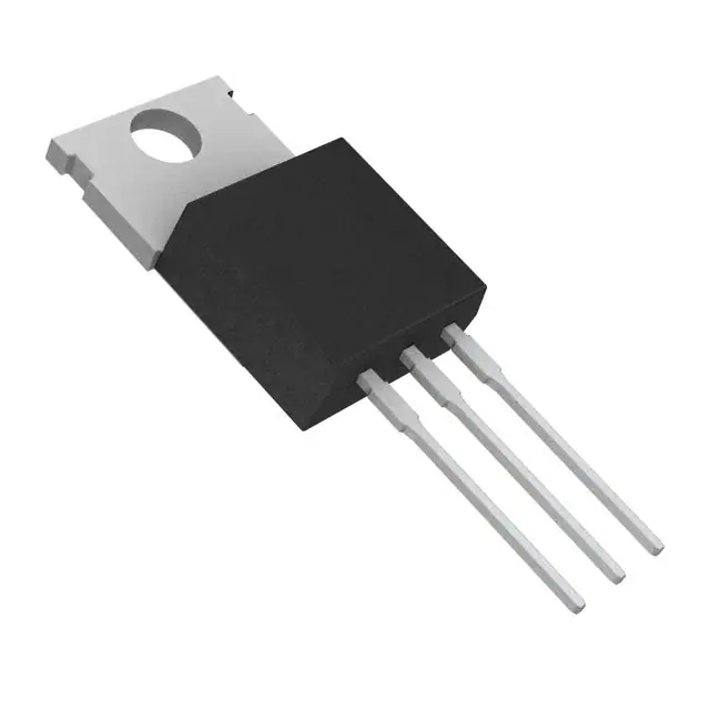
TO−220AB
CASE 221A
STYLE 1
1
2
3
MARKING DIAGRAM
& PIN ASSIGNMENT
4
Collector
Stresses exceeding Maximum Ratings may damage the device. Maximum
Ratings are stress ratings only. Functional operation above the Recommended
Operating Conditions is not implied. Extended exposure to stresses above the
Recommended Operating Conditions may affect device reliability.
THERMAL CHARACTERISTICS
Characteristic
Thermal Resistance,
Junction−to−Case
Thermal Resistance,
Junction−to−Ambient
Maximum Lead Temperature for Soldering
Purposes: 1/8 in from Case for 5 Sec
Symbol
Max
Unit
RqJC
4.2
°C/W
RqJA
75
°C/W
TL
275
°C
1. Pulse Width v 6.0 ms, Duty Cycle v 50%.
D4xC12G
AYWW
1
Base
3
Emitter
2
Collector
x
A
Y
WW
G
= 4 or 5
= Assembly Location
= Year
= Work Week
= Pb−Free Package
ORDERING INFORMATION
*For additional information on our Pb−Free strategy and soldering details, please
download the ON Semiconductor Soldering and Mounting Techniques
Reference Manual, SOLDERRM/D.
© Semiconductor Components Industries, LLC, 2011
October, 2011 − Rev. 3
1
See detailed ordering and shipping information in the package
dimensions section on page 2 of this data sheet.
Publication Order Number:
D45C12/D
�D45C12 (PNP), D44C12 (NPN)
ÎÎÎÎÎÎÎÎÎÎÎÎÎÎÎÎÎÎÎÎÎÎÎÎÎÎÎÎÎÎÎÎÎ
ÎÎÎÎÎÎÎÎÎÎÎÎÎÎÎÎÎÎÎÎÎÎÎÎÎÎÎÎÎÎÎÎÎ
ÎÎÎÎÎÎÎÎÎÎÎÎÎÎÎÎÎÎÎÎÎÎÎÎÎÎÎÎÎÎÎÎÎ
ÎÎÎÎÎÎÎÎÎÎÎÎÎÎÎÎÎÎÎÎÎÎ
ÎÎÎÎÎÎÎÎÎÎÎÎÎÎÎ
ÎÎÎÎÎÎÎÎÎÎÎÎÎÎÎÎÎÎÎÎÎÎ
ÎÎÎÎ
ÎÎÎÎ
ÎÎÎÎ
ÎÎÎ
ÎÎÎÎÎÎÎÎÎÎÎÎÎÎÎÎÎÎÎÎÎÎÎÎÎÎÎÎÎÎÎÎÎÎÎÎÎ
ÎÎÎÎÎÎÎÎÎÎÎÎÎÎÎÎÎÎÎÎÎÎ
ÎÎÎÎ
ÎÎÎÎ
ÎÎÎÎ
ÎÎÎ
ÎÎÎÎÎÎÎÎÎÎÎÎÎÎÎÎÎÎÎÎÎÎÎÎÎÎÎÎÎÎÎÎÎÎÎÎÎ
ÎÎÎÎÎÎÎÎÎÎÎÎÎÎÎÎÎÎÎÎÎÎÎÎÎÎÎÎÎÎÎÎÎ
ÎÎÎÎÎÎÎÎÎÎÎÎÎÎÎÎÎÎÎÎÎÎÎÎÎÎÎÎÎÎÎÎÎ
ÎÎÎÎÎÎÎÎÎÎÎÎÎÎÎÎÎÎÎÎÎÎ
ÎÎÎÎÎÎÎÎÎÎÎÎÎÎÎÎ
ÎÎÎÎÎÎÎÎÎÎÎÎÎÎÎÎÎÎÎÎÎÎÎÎÎÎÎÎÎÎÎÎÎÎÎÎÎÎ
ÎÎÎÎÎÎÎÎÎÎÎÎÎÎÎÎÎÎÎÎÎÎÎÎÎÎÎÎÎÎÎÎÎ
ÎÎÎÎÎÎÎÎÎÎÎÎÎÎÎÎÎÎÎÎÎÎÎÎÎÎÎÎÎÎÎÎÎ
ÎÎÎÎÎÎÎÎÎÎÎÎÎÎÎÎÎÎÎÎÎÎ
ÎÎÎÎÎÎÎÎÎÎÎÎÎÎÎÎ
ÎÎÎÎÎÎÎÎÎÎÎÎÎÎÎÎÎÎÎÎÎÎÎÎÎÎÎÎÎÎÎÎÎÎÎÎÎÎ
ÎÎÎÎÎÎÎÎÎÎÎÎÎÎÎÎÎÎÎÎÎÎÎÎÎÎÎÎÎÎÎÎÎÎÎÎÎÎ
ÎÎÎÎÎÎÎÎÎÎÎÎÎÎÎÎÎÎÎÎÎÎÎÎÎÎÎÎÎÎÎÎÎÎÎÎÎÎ
ÎÎÎÎÎÎÎÎÎÎÎÎÎÎÎÎÎÎÎÎÎÎÎÎÎÎÎÎÎÎÎÎÎ
ÎÎÎÎÎÎÎÎÎÎÎÎÎÎÎÎÎÎÎÎÎÎÎÎÎÎÎÎÎÎÎÎÎ
ÎÎÎÎÎÎÎÎÎÎÎÎÎÎÎÎÎÎÎÎÎÎ
ÎÎÎÎÎÎÎÎÎÎÎÎÎÎÎÎ
ÎÎÎÎÎÎÎÎÎÎÎÎÎÎÎÎÎÎÎÎÎÎÎÎÎÎÎÎÎÎÎÎÎÎÎÎÎÎ
ÎÎÎÎÎÎÎÎÎÎÎÎÎÎÎÎÎÎÎÎÎÎÎÎÎÎÎÎÎÎÎÎÎÎÎÎÎÎ
ÎÎÎÎÎÎÎÎÎÎÎÎÎÎÎÎÎÎÎÎÎÎÎÎÎÎÎÎÎÎÎÎÎ
ÎÎÎÎÎÎÎÎÎÎÎÎÎÎÎÎÎÎÎÎÎÎÎÎÎÎÎÎÎÎÎÎÎ
ÎÎÎÎÎÎÎÎÎÎÎÎÎÎÎÎÎÎÎÎÎÎ
ÎÎÎÎÎÎÎÎÎÎÎÎÎÎÎÎ
ÎÎÎÎÎÎÎÎÎÎÎÎÎÎÎÎÎÎÎÎÎÎ
ÎÎÎÎ
ÎÎÎ
ÎÎÎ
ÎÎÎ
ÎÎÎ
ÎÎÎÎÎÎÎÎÎÎÎÎÎÎÎÎÎÎÎÎÎÎÎÎÎÎÎÎÎÎÎÎÎÎÎÎÎÎ
ÎÎÎÎÎÎÎÎÎÎÎÎÎÎÎÎÎÎÎÎÎÎÎÎÎÎÎÎÎÎÎÎÎ
ÎÎÎÎÎÎÎÎÎÎÎÎÎÎÎÎÎÎÎÎÎÎÎÎÎÎÎÎÎÎÎÎÎ
ÎÎÎÎÎÎÎÎÎÎÎÎÎÎÎÎÎÎÎÎÎÎÎÎÎÎÎÎÎÎÎÎÎ
ÎÎÎÎÎÎÎÎÎÎÎÎÎÎÎÎÎÎÎÎÎÎ
ÎÎÎÎÎÎÎÎÎÎÎÎÎÎÎÎ
ÎÎÎÎÎÎÎÎÎÎÎÎÎÎÎÎÎÎÎÎÎÎÎÎÎÎÎÎÎÎÎÎÎÎÎÎÎÎ
ÎÎÎÎÎÎÎÎÎÎÎÎÎÎÎÎÎÎÎÎÎÎÎÎÎÎÎÎÎÎÎÎÎÎÎÎÎÎ
ÎÎÎÎÎÎÎÎÎÎÎÎÎÎÎÎÎÎÎÎÎÎÎÎÎÎÎÎÎÎÎÎÎÎÎÎÎÎ
ELECTRICAL CHARACTERISTICS (TJ = 25°C unless otherwise noted)
Characteristic
Symbol
DC Current Gain
(VCE = 1.0 Vdc, IC = 0.2 Adc)
(VCE = 1.0 Vdc, IC = 1.0 Adc)
(VCE = 1.0 Vdc, IC = 2.0 Adc)
Min
Max
40
20
20
120
−
−
Unit
hFE
−
ELECTRICAL CHARACTERISTICS (TC = 25°C unless otherwise noted)
Characteristic
Symbol
Min
Typ
Max
Unit
Collector Cutoff Current (VCE = Rated VCES, VBE = 0)
ICES
−
−
0.1
mA
Emitter Cutoff Current (VEB = 5.0 Vdc)
IEBO
−
−
10
mA
Collector−Emitter Saturation Voltage (IC = 1.0 Adc, IB = 50 mAdc)
VCE(sat)
−
0.135
0.5
Vdc
Base−Emitter Saturation Voltage (IC = 1.0 Adc, IB = 100 mAdc)
VBE(sat)
−
0.85
1.3
Vdc
Ccb
−
125
−
pF
fT
−
40
−
MHz
td + tr
−
50
75
ns
Storage Time (IC = 1.0 Adc, IB1 = IB2 = 0.1 Adc)
ts
−
350
550
ns
Fall Time (IC = 1.0 Adc, IB1 = IB2 = 0.1 Adc)
tf
−
50
75
ns
OFF CHARACTERISTICS
ON CHARACTERISTICS
DYNAMIC CHARACTERISTICS
Collector Capacitance (VCB = 10 Vdc, f = 1.0 MHz)
Gain Bandwidth Product (IC = 20 mA, VCE = 4.0 Vdc, f = 20 MHz)
SWITCHING TIMES
Delay and Rise Times (IC = 1.0 Adc, IB1 = 0.1 Adc)
ORDERING INFORMATION
Device
Shipping†
Package
D45C12
TO−220AB
D45C12G
TO−220AB
(Pb−Free)
D44C12
TO−220AB
D44C12G
TO−220AB
(Pb−Free)
50 Units / Rail
†For information on tape and reel specifications, including part orientation and tape sizes, please refer to our Tape and Reel Packaging
Specifications Brochure, BRD8011/D.
200
IC, COLLECTOR CURRENT (AMPS)
hFE, DC CURRENT GAIN
VCE = 1.0 Vdc
TJ = 25°C
100
90
80
70
60
50
40
30
20
0.04
0.07 0.1
0.2 0.3 0.4
0.7 1.0
IC, COLLECTOR CURRENT (AMPS)
2.0
10
5.0
3.0
2.0
0.1 ms
dc
1.0
0.5
0.3
0.2
0.1
1.0 ms
TC ≤ 70°C
DUTY CYCLE ≤ 50%
0.05
0.03
0.02
0.01
1.0
3.0 4.0
1.0 ms
10 ms
Figure 1. Typical DC Current Gain
50
5.0 7.0 10
20 30
2.0 3.0
VCE, COLLECTOR-EMITTER VOLTAGE (VOLTS)
70 100
Figure 2. Maximum Rated Forward Bias
Safe Operating Area
http://onsemi.com
2
�MECHANICAL CASE OUTLINE
PACKAGE DIMENSIONS
TO−220
CASE 221A
ISSUE AK
DATE 13 JAN 2022
SCALE 1:1
STYLE 1:
PIN 1.
2.
3.
4.
BASE
COLLECTOR
EMITTER
COLLECTOR
STYLE 2:
PIN 1.
2.
3.
4.
BASE
EMITTER
COLLECTOR
EMITTER
STYLE 3:
PIN 1.
2.
3.
4.
CATHODE
ANODE
GATE
ANODE
STYLE 4:
PIN 1.
2.
3.
4.
MAIN TERMINAL 1
MAIN TERMINAL 2
GATE
MAIN TERMINAL 2
STYLE 5:
PIN 1.
2.
3.
4.
GATE
DRAIN
SOURCE
DRAIN
STYLE 6:
PIN 1.
2.
3.
4.
ANODE
CATHODE
ANODE
CATHODE
STYLE 7:
PIN 1.
2.
3.
4.
CATHODE
ANODE
CATHODE
ANODE
STYLE 8:
PIN 1.
2.
3.
4.
CATHODE
ANODE
EXTERNAL TRIP/DELAY
ANODE
STYLE 9:
PIN 1.
2.
3.
4.
GATE
COLLECTOR
EMITTER
COLLECTOR
STYLE 10:
PIN 1.
2.
3.
4.
GATE
SOURCE
DRAIN
SOURCE
STYLE 11:
PIN 1.
2.
3.
4.
DRAIN
SOURCE
GATE
SOURCE
STYLE 12:
PIN 1.
2.
3.
4.
MAIN TERMINAL 1
MAIN TERMINAL 2
GATE
NOT CONNECTED
DOCUMENT NUMBER:
DESCRIPTION:
98ASB42148B
TO−220
Electronic versions are uncontrolled except when accessed directly from the Document Repository.
Printed versions are uncontrolled except when stamped “CONTROLLED COPY” in red.
PAGE 1 OF 1
onsemi and
are trademarks of Semiconductor Components Industries, LLC dba onsemi or its subsidiaries in the United States and/or other countries. onsemi reserves
the right to make changes without further notice to any products herein. onsemi makes no warranty, representation or guarantee regarding the suitability of its products for any particular
purpose, nor does onsemi assume any liability arising out of the application or use of any product or circuit, and specifically disclaims any and all liability, including without limitation
special, consequential or incidental damages. onsemi does not convey any license under its patent rights nor the rights of others.
© Semiconductor Components Industries, LLC, 2019
www.onsemi.com
�onsemi,
, and other names, marks, and brands are registered and/or common law trademarks of Semiconductor Components Industries, LLC dba “onsemi” or its affiliates
and/or subsidiaries in the United States and/or other countries. onsemi owns the rights to a number of patents, trademarks, copyrights, trade secrets, and other intellectual property.
A listing of onsemi’s product/patent coverage may be accessed at www.onsemi.com/site/pdf/Patent−Marking.pdf. onsemi reserves the right to make changes at any time to any
products or information herein, without notice. The information herein is provided “as−is” and onsemi makes no warranty, representation or guarantee regarding the accuracy of the
information, product features, availability, functionality, or suitability of its products for any particular purpose, nor does onsemi assume any liability arising out of the application or use
of any product or circuit, and specifically disclaims any and all liability, including without limitation special, consequential or incidental damages. Buyer is responsible for its products
and applications using onsemi products, including compliance with all laws, regulations and safety requirements or standards, regardless of any support or applications information
provided by onsemi. “Typical” parameters which may be provided in onsemi data sheets and/or specifications can and do vary in different applications and actual performance may
vary over time. All operating parameters, including “Typicals” must be validated for each customer application by customer’s technical experts. onsemi does not convey any license
under any of its intellectual property rights nor the rights of others. onsemi products are not designed, intended, or authorized for use as a critical component in life support systems
or any FDA Class 3 medical devices or medical devices with a same or similar classification in a foreign jurisdiction or any devices intended for implantation in the human body. Should
Buyer purchase or use onsemi products for any such unintended or unauthorized application, Buyer shall indemnify and hold onsemi and its officers, employees, subsidiaries, affiliates,
and distributors harmless against all claims, costs, damages, and expenses, and reasonable attorney fees arising out of, directly or indirectly, any claim of personal injury or death
associated with such unintended or unauthorized use, even if such claim alleges that onsemi was negligent regarding the design or manufacture of the part. onsemi is an Equal
Opportunity/Affirmative Action Employer. This literature is subject to all applicable copyright laws and is not for resale in any manner.
PUBLICATION ORDERING INFORMATION
LITERATURE FULFILLMENT:
Email Requests to: orderlit@onsemi.com
onsemi Website: www.onsemi.com
◊
TECHNICAL SUPPORT
North American Technical Support:
Voice Mail: 1 800−282−9855 Toll Free USA/Canada
Phone: 011 421 33 790 2910
Europe, Middle East and Africa Technical Support:
Phone: 00421 33 790 2910
For additional information, please contact your local Sales Representative
�