Is Now Part of
To learn more about ON Semiconductor, please visit our website at
www.onsemi.com
Please note: As part of the Fairchild Semiconductor integration, some of the Fairchild orderable part numbers
will need to change in order to meet ON Semiconductor’s system requirements. Since the ON Semiconductor
product management systems do not have the ability to manage part nomenclature that utilizes an underscore
(_), the underscore (_) in the Fairchild part numbers will be changed to a dash (-). This document may contain
device numbers with an underscore (_). Please check the ON Semiconductor website to verify the updated
device numbers. The most current and up-to-date ordering information can be found at www.onsemi.com. Please
email any questions regarding the system integration to Fairchild_questions@onsemi.com.
ON Semiconductor and the ON Semiconductor logo are trademarks of Semiconductor Components Industries, LLC dba ON Semiconductor or its subsidiaries in the United States and/or other countries. ON Semiconductor owns the rights to a number
of patents, trademarks, copyrights, trade secrets, and other intellectual property. A listing of ON Semiconductor’s product/patent coverage may be accessed at www.onsemi.com/site/pdf/Patent-Marking.pdf. ON Semiconductor reserves the right
to make changes without further notice to any products herein. ON Semiconductor makes no warranty, representation or guarantee regarding the suitability of its products for any particular purpose, nor does ON Semiconductor assume any liability
arising out of the application or use of any product or circuit, and specifically disclaims any and all liability, including without limitation special, consequential or incidental damages. Buyer is responsible for its products and applications using ON
Semiconductor products, including compliance with all laws, regulations and safety requirements or standards, regardless of any support or applications information provided by ON Semiconductor. “Typical” parameters which may be provided in ON
Semiconductor data sheets and/or specifications can and do vary in different applications and actual performance may vary over time. All operating parameters, including “Typicals” must be validated for each customer application by customer’s
technical experts. ON Semiconductor does not convey any license under its patent rights nor the rights of others. ON Semiconductor products are not designed, intended, or authorized for use as a critical component in life support systems or any FDA
Class 3 medical devices or medical devices with a same or similar classification in a foreign jurisdiction or any devices intended for implantation in the human body. Should Buyer purchase or use ON Semiconductor products for any such unintended
or unauthorized application, Buyer shall indemnify and hold ON Semiconductor and its officers, employees, subsidiaries, affiliates, and distributors harmless against all claims, costs, damages, and expenses, and reasonable attorney fees arising out
of, directly or indirectly, any claim of personal injury or death associated with such unintended or unauthorized use, even if such claim alleges that ON Semiconductor was negligent regarding the design or manufacture of the part. ON Semiconductor
is an Equal Opportunity/Affirmative Action Employer. This literature is subject to all applicable copyright laws and is not for resale in any manner.
�DF005S - DF10S
Bridge Rectifiers
Features
Description
• Maximum Surge Rating: IFSM = 50 A
I2t = 10 A2Sec
• Optimized VF: Typical 0.94 V at 1.5 A, 25°C
• Glass Passivated Junctions
• Lead Free Compliant to EU RoHS 2002/95/EU Directives
• Green Molding Compound: IEC61249
• Qualified with IR Reflow and Wave Soldering
• UL Certified, UL #E258596
With the ever-pressing need to improve power supply
efficiency, improve surge rating, improve reliability, and
reduce size, the DFxS family sets a standard in performance.
The design offers an surge rating of 50 A. This is important when improving reliability and increasing efficiency.
High efficiency designs strive to reduce circuit resistance, which, unfortunately can result in increased
inrush surge. As such high surge current ratings can be
required to maintain or improve reliability.
The design also offers better efficiency by achieving a
1.5 A VF of 1.1 V maximum at 25°C. This lower VF also
supports cooler and more efficient operation.
Finally, the DFxS achieves all this in a SDIP surface
mount form factor, reducing board space and volumetric
requirements vs. competitive devices.
~
+
IN
OUT
~
-
SDIP
Ordering Information
Part Number
Top Mark
Package
Packing Method
DF005S
DF005S
SDIP 4L
Tape and Reel
DF01S
DF01S
SDIP 4L
Tape and Reel
DF02S
DF02S
SDIP 4L
Tape and Reel
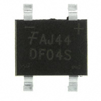
DF04S
DF04S
SDIP 4L
Tape and Reel
DF06S
DF06S
SDIP 4L
Tape and Reel
DF08S
DF08S
SDIP 4L
Tape and Reel
DF10S
DF10S
SDIP 4L
Tape and Reel
© 1998 Fairchild Semiconductor Corporation
DF005S - DF10S Rev. 1.5
www.fairchildsemi.com
DF005S - DF10S — Bridge Rectifiers
May 2015
�Stresses exceeding the absolute maximum ratings may damage the device. The device may not function or be operable above the recommended operating conditions and stressing the parts to these levels is not recommended. In addition, extended exposure to stresses above the recommended operating conditions may affect device reliability. The
absolute maximum ratings are stress ratings only. Values are at TA = 25°C unless otherwise noted.
Value
Symbol
Parameter
VRRM
Maximum Repetitive Reverse Voltage
50
100
200
400
600
800
1000
V
VRMS
Maximum RMS Bridge Input Voltage
35
70
140
280
420
560
700
V
VDC
DC Reverse Voltage at Rated IR
50
100
200
400
600
800
1000
V
IF(AV)
Average Rectified Forward Current
at TA = 40°C
1.5
A
IFSM
Non-Repetitive Peak Forward Surge
Current
8.3 ms Single Half-Sine Wave
50
A
TSTG
Storage Temperature Range
-55 to +150
°C
Operating Junction Temperature
-55 to +150
°C
TJ
DF005S DF01S DF02S DF04S DF06S DF08S DF10S
Unit
Thermal Characteristics
Values are at TA = 25°C unless otherwise noted.
Symbol
PD
Parameter
Power Dissipation
Value
Unit
3.1
W
(1)
Thermal Resistance,
Junction-to-Ambient
RθJA
Thermal Characterization
Parameter, Junction to Lead
ψJL
Single-Die Measurement
(Maximum Land Pattern: 13 x 13 mm)
62
Multi-Die Measurement(2)
(Maximum Land Pattern: 13 x 13 mm)
50
Multi-Die Measurement(2)
(Minimum Land Pattern: 1.3 x 1.5 mm)
105
Single-Die Measurement(2)
(Maximum and Minimum Land Pattern)
27
°C/W
°C/W
Notes:
1. Device mounted on PCB with 0.5 inch × 0.5 inch (13 mm × 13 mm).
2. The thermal resistances (RθJA & ψJL) are characterized with the device mounted on the following FR4 printed circuit
boards, as shown in Figure 1 and Figure 2. PCB size: 76.2 x 114.3 mm.
Heating effect from adjacent dice is considered and only two dices are powered at the same time.
F
S
S
F
F
S
S
F
Figure 2. Minimum Pads of 2 oz Copper
Figure 1. Maximum Pads of 2 oz Copper
© 1998 Fairchild Semiconductor Corporation
DF005S - DF10S Rev. 1.5
www.fairchildsemi.com
2
DF005S - DF10S — Bridge Rectifiers
Absolute Maximum Ratings
�Values are at TA = 25°C unless otherwise noted.
Symbol
VF
Parameter
Forward Voltage, per Element
IR
Reverse Current, per Element at Rated VR
I2t
Rating for Fusing (t < 8.35 ms)
CJ
Typical Capacitance, per Leg
© 1998 Fairchild Semiconductor Corporation
DF005S - DF10S Rev. 1.5
Conditions
Min.
Typ.
Max.
Unit
V
IF = 1.5 A
1.1
TA = 25°C
5.0
TA = 125°C
500
10
VR = 4.0 V,
f = 1.0 MHz
25
μA
A2s
pF
www.fairchildsemi.com
3
DF005S - DF10S — Bridge Rectifiers
Electrical Characteristics
�Average Rectified Forward Current, IF [A]
Peak Forward Surge Current, IFSM [A]
50
40
30
20
10
0
1
2
5
10
20
Number of Cycles at 60Hz
50
100
1
0.5
Based on RθJA, per Leg
0
20
40
60
80
100
120
Ambient Temperature [ºC]
140
160
Figure 4. Forward Current Derating Curve
Figure 3. Non-Repetitive Surge Current
100
Reverse Current, IR[μA]
10
Forward Current, IF[A]
1.5
1
o
TJ=150 C
0.1
o
TJ=25 C
o
TJ=125 C
10
o
TJ=125 C
o
TJ=150 C
1
o
TJ=25 C
0.1
0.01
o
TJ=-55 C
o
TJ= -55 C
0.01
0.2
0.3
0.4
0.5
0.6
0.7
0.8
0.9
1.0
1.1
1E-3
200
1.2
Forward Voltage Drop, VF[V]
400
500
600
700
800
900
1000
Reverse Voltage, VR[V]
Figure 5. Forward Voltage Characteristics
© 1998 Fairchild Semiconductor Corporation
DF005S - DF10S Rev. 1.5
300
Figure 6. Reverse Current vs. Reverse Voltage
www.fairchildsemi.com
4
DF005S - DF10S — Bridge Rectifiers
Typical Performance Characteristics
�DF005S - DF10S — Bridge Rectifiers
Physical Dimensions
�����
�����
�
����
�
����
3,1��,'
237,21$/
�����
�����
�
������
�����
�����
�
�����
�����
����
723�9,(:
&+$0)(5
237,21$/
/$1'�3$77(51�5(&200(1'$7,21
�����
�����
�����
�����
����
����
�����
�����
�����
�����
����
6,'(�9,(:
�����
�����
(1'�9,(:
127(6�
��$��7+,6�3$&.$*(�'2(6�127�&21)250�72�
$1