DATA SHEET
www.onsemi.com
Bridge Rectifiers
DF005S - DF10S
Description
With the ever−pressing need to improve power supply efficiency,
improve surge rating, improve reliability, and reduce size, the DFxS
family sets a standard in performance.
The design offers an surge rating of 50 A. This is important when
improving reliability and increasing efficiency. High efficiency
designs strive to reduce circuit resistance, which, unfortunately can
result in increased inrush surge. As such high surge current ratings can
be required to maintain or improve reliability.
The design also offers better efficiency by achieving a 1.5 A VF of
1.1 V maximum at 25°C. This lower VF also supports cooler and more
efficient operation.
Finally, the DFxS achieves all this in a SDIP surface mount form
factor, reducing board space and volumetric requirements vs.
competitive devices.
PDIP−4 GW
CASE 709AE
̃
+
IN
OUT
̃
−
SDIP
MARKING DIAGRAM
Features
•
•
•
•
•
•
•
Maximum Surge Rating: IFSM = 50 A, I2t = 10 A2Sec
Optimized VF: Typical 0.94 V at 1.5 A, 25°C
Glass Passivated Junctions
Lead Free Compliant to EU RoHS 2002/95/EU Directives
Green Molding Compound: IEC61249
Qualified with IR Reflow and Wave Soldering
UL Certified, UL #E258596
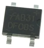
ON
ZXYY
DF06M
Z
= Subcon Assembly Plant Code
X
= Last Digit of Calendar Year
YY
= Weekly Payweek Date code
DFXXXM = Specific Device Number
xxx = 01, 02, 04, 06, 08, 10, or 005
ORDERING INFORMATION
See detailed ordering and shipping information on page 4 of
this data sheet.
© Semiconductor Components Industries, LLC, 2013
March, 2022 − Rev 2
1
Publication Order Number:
DF10S/D
�DF005S − DF10S
ABSOLUTE MAXIMUM RATINGS (Note 3) Values are at TA = 25°C unless otherwise noted.
Value
Symbol
Parameter
DF005S
DF01S
DF02S
DF04S
DF06S
DF08S
DF10S
Unit
VRRM
Maximum Repetitive Reverse Voltage
50
100
200
400
600
800
1000
V
VRMS
Maximum RMS Bridge Input Voltage
35
70
140
280
420
560
700
V
50
100
200
400
600
800
1000
V
VDC
DC Reverse Voltage at Rated IR
IF(AV)
Average Rectified Forward Current at TA = 40°C
1.5
A
IFSM
Non−Repetitive Peak Forward Surge Current
8.3 ms Single Half−Sine Wave
50
A
TSTG
Storage Temperature Range
−55 to +150
°C
Operating Junction Temperature
−55 to +150
°C
TJ
Stresses exceeding those listed in the Maximum Ratings table may damage the device. If any of these limits are exceeded, device functionality
should not be assumed, damage may occur and reliability may be affected.
THERMAL CHARACTERISTICS Values are at TA = 25°C unless otherwise noted.
Symbol
PD
Parameter
Value
Unit
3.1
W
Single−Die Measurement (Note 1)
(Maximum Land Pattern: 13 x 13 mm)
62
°C/W
Multi−Die Measurement (Note 2)
(Maximum Land Pattern: 13 x 13 mm)
50
Multi−Die Measurement (Note 2)
(Minimum Land Pattern: 1.3 x 1.5 mm)
105
Single−Die Measurement (Note 2)
(Maximum and Minimum Land Pattern)
27
Power Dissipation
RθJA
Thermal Resistance,
Junction−to−Ambient
Thermal Characterization
Parameter, Junction to Lead
ψJL
°C/W
1. Device mounted on PCB with 0.5 inch x 0.5 inch (13 mm x 13 mm). Minimum Pads of 2 oz Copper.
2. The thermal resistances (RθJA & ψJL) are characterized with the device mounted on the following FR4 printed circuit boards, as shown in
Figure 1 and Figure 2. PCB size: 76.2 x 114.3 mm. Heating effect from adjacent dice is considered and only tow dices are powered at the
same time.
F
S
S
F
F
S
S
F
Figure 1. Maximum pads of 2 oz copper
Figure 2. Minimun pads of 2 oz copper
ELECTRICAL CHARACTERISTICS
Values are at TA = 25°C unless otherwise noted.
Symbol
Min.
Typ.
Max.
Unit
VF
Forward Voltage, per Element
Parameter
IF = 1.5 A
−
−
1.1
V
IR
Reverse Current, per Element at Rated VR
TA = 25°C
−
−
5.0
mA
TA = 125_C
−
−
500
−
−
−
10
A2s
VR = 4.0 V,
f = 1.0 MHz
−
25
−
pF
I2t
Rating for Fusing (t < 8.35 ms)
CJ
Typical Capacitance, per Leg
Conditions
Product parametric performance is indicated in the Electrical Characteristics for the listed test conditions, unless otherwise noted. Product
performance may not be indicated by the Electrical Characteristics if operated under different conditions.
www.onsemi.com
2
�DF005S − DF10S
Peak Forward Surge Current, IFSM [A]
50
40
30
20
10
0
1
2
5
10
20
50
100
Average Rectified Forward Current, IF [A]
TYPICAL CHARACTERISTICS
1.5
1
0.5
Based on RqJA, per Leg
0
20
40
Number of Cycles at 60 Hz
Figure 3. Non−Repetitive Surge Current
140
160
Figure 4. Forward Current Derating Curve
100
Reverse Current, IR [ mA]
10
Forward Current, IF [A]
60
80
100
120
Ambient Temperature [5C]
1
TJ = 150°C
0.1
TJ = 25°C
TJ = 125°C
10
TJ=150°C
1
TJ=25°C
0.1
0.01
TJ=−55°C
TJ=−55°C
0.01
0.2
0.3
0.4
0.5
0.6
0.7
0.8
0.9
1.0
1.1
1.2
0.001
200
Forward Voltage Drop, VF [V]
Figure 5. Forward Voltage Characteristics
TJ=125°C
300
500
400
600
700 800
Reverse Voltage Drop, VR [V]
900 1000
Figure 6. Reverse Current vs. Reverse Voltage
www.onsemi.com
3
�DF005S − DF10S
ORDERING INFORMATION
Product Number
Device Code Marking
Package
Shipping†
DF005S
DF005S
PDIP−4, GW
(Pb−Free, Halide Free)
1500 / Tape and Reel
DF01S
DF01S
PDIP−4, GW
(Pb−Free, Halide Free)
1500 / Tape and Reel
DF02S
DF02S
PDIP−4, GW
(Pb−Free, Halide Free)
1500 / Tape and Reel
DF04S
DF04S
PDIP−4 GW
(Pb−Free, Halide Free)
1500 / Tape and Reel
DF06S
DF06S
PDIP−4, GW
(Pb−Free, Halide Free)
1500 / Tape and Reel
DF08S
DF08S
PDIP−4, GW
(Pb−Free, Halide Free)
1500 / Tape and Reel
DF10S
DF10S
PDIP−4, GW
(Pb−Free, Halide Free)
1500 / Tape and Reel
†For information on tape and reel specifications, including part orientation and tape sizes, please refer to our Tape and Reel Packaging
Specifications Brochure, BRD8011/D.
www.onsemi.com
4
�MECHANICAL CASE OUTLINE
PACKAGE DIMENSIONS
PDIP4 GW
CASE 709AE
ISSUE O
DATE 31 JUL 2016
5.200
5.000
4
1.30
3
1.50
PIN1 ID
OPTIONAL
6.500
6.200
1
10.300
9.400
10.40
2
1.200
0.890
5.10
TOP VIEW
LAND PATTERN RECOMMENDATION
7.874
7.370
8.510
8.050
CHAMFER
OPTIONAL
2.60
2.20
1.12
SIDE VIEW
0.330
0.220
1.530
1.020
0.330
0.076
END VIEW
NOTES:
A. THIS PACKAGE DOES NOT CONFORM TO
ANY REFERENCE STANDARD.
B. ALL DIMENSIONS ARE IN MILLIMETERS.
C. DIMENSIONS ARE EXCLUSIVE OF BURRS,
MOLD FLASH AND TIE BAR PROTRUSIONS.
DOCUMENT NUMBER:
DESCRIPTION:
98AON13473G
PDIP4 GW
Electronic versions are uncontrolled except when accessed directly from the Document Repository.
Printed versions are uncontrolled except when stamped “CONTROLLED COPY” in red.
PAGE 1 OF 1
onsemi and
are trademarks of Semiconductor Components Industries, LLC dba onsemi or its subsidiaries in the United States and/or other countries. onsemi reserves
the right to make changes without further notice to any products herein. onsemi makes no warranty, representation or guarantee regarding the suitability of its products for any particular
purpose, nor does onsemi assume any liability arising out of the application or use of any product or circuit, and specifically disclaims any and all liability, including without limitation
special, consequential or incidental damages. onsemi does not convey any license under its patent rights nor the rights of others.
© Semiconductor Components Industries, LLC, 2016
www.onsemi.com
�onsemi,
, and other names, marks, and brands are registered and/or common law trademarks of Semiconductor Components Industries, LLC dba “onsemi” or its affiliates
and/or subsidiaries in the United States and/or other countries. onsemi owns the rights to a number of patents, trademarks, copyrights, trade secrets, and other intellectual property.
A listing of onsemi’s product/patent coverage may be accessed at www.onsemi.com/site/pdf/Patent−Marking.pdf. onsemi reserves the right to make changes at any time to any
products or information herein, without notice. The information herein is provided “as−is” and onsemi makes no warranty, representation or guarantee regarding the accuracy of the
information, product features, availability, functionality, or suitability of its products for any particular purpose, nor does onsemi assume any liability arising out of the application or use
of any product or circuit, and specifically disclaims any and all liability, including without limitation special, consequential or incidental damages. Buyer is responsible for its products
and applications using onsemi products, including compliance with all laws, regulations and safety requirements or standards, regardless of any support or applications information
provided by onsemi. “Typical” parameters which may be provided in onsemi data sheets and/or specifications can and do vary in different applications and actual performance may
vary over time. All operating parameters, including “Typicals” must be validated for each customer application by customer’s technical experts. onsemi does not convey any license
under any of its intellectual property rights nor the rights of others. onsemi products are not designed, intended, or authorized for use as a critical component in life support systems
or any FDA Class 3 medical devices or medical devices with a same or similar classification in a foreign jurisdiction or any devices intended for implantation in the human body. Should
Buyer purchase or use onsemi products for any such unintended or unauthorized application, Buyer shall indemnify and hold onsemi and its officers, employees, subsidiaries, affiliates,
and distributors harmless against all claims, costs, damages, and expenses, and reasonable attorney fees arising out of, directly or indirectly, any claim of personal injury or death
associated with such unintended or unauthorized use, even if such claim alleges that onsemi was negligent regarding the design or manufacture of the part. onsemi is an Equal
Opportunity/Affirmative Action Employer. This literature is subject to all applicable copyright laws and is not for resale in any manner.
PUBLICATION ORDERING INFORMATION
LITERATURE FULFILLMENT:
Email Requests to: orderlit@onsemi.com
onsemi Website: www.onsemi.com
◊
TECHNICAL SUPPORT
North American Technical Support:
Voice Mail: 1 800−282−9855 Toll Free USA/Canada
Phone: 011 421 33 790 2910
Europe, Middle East and Africa Technical Support:
Phone: 00421 33 790 2910
For additional information, please contact your local Sales Representative
�