Revised June 2001
DM74150
Data Selectors/Multiplexers
General Description
Features
These data selectors/multiplexers contain full on-chip
decoding to select the desired data source. The DM74150
selects one-of-sixteen data sources. The DM74150 has a
strobe input which must be at a LOW logic level to enable
these devices. A HIGH level at the strobe forces the W output HIGH and the Y output (as applicable) LOW.
■ 150 selects one-of-sixteen data lines
The DM74150 features an inverted (W) output only.
■ Performs parallel-to-serial conversion
■ Permits multiplexing from N lines to one line
■ Also for use as Boolean function generator
■ Typical average propagation delay time, data input to W
output: 11 ns
■ Typical power dissipation: 200 mW
Ordering Code:
Order Number
DM74150N
Package Number
N24A
Package Description
24-Lead Plastic Dual-In-Line Package (PDIP), JEDEC MS-011, 0.600" Wide
Connection Diagram
Function Table
Inputs
Outputs
Select
Strobe
W
D
C
B
A
S
X
X
X
X
H
H
L
L
L
L
L
E0
L
L
L
H
L
E1
L
L
H
L
L
E2
L
L
H
H
L
E3
L
H
L
L
L
E4
L
H
L
H
L
E5
L
H
H
L
L
E6
L
H
H
H
L
E7
H
L
L
L
L
E8
H
L
L
H
L
E9
H
L
H
L
L
E10
H
L
H
H
L
E11
H
H
L
L
L
E12
H
H
L
H
L
E13
H
H
H
L
L
E14
H
H
H
H
L
E15
H = HIGH Level
L = LOW Level
X = Don’t Care
E0, E1 …E15 = the complement of the level of the respective E input
© 2001 Fairchild Semiconductor Corporation
DS006546
www.fairchildsemi.com
DM74150 Data Selectors/Multiplexers
September 1986
�DM74150
Logic Diagram
www.fairchildsemi.com
2
�Supply Voltage
Note 1: The “Absolute Maximum Ratings” are those values beyond which
the safety of the device cannot be guaranteed. The device should not be
operated at these limits. The parametric values defined in the Electrical
Characteristics tables are not guaranteed at the absolute maximum ratings.
The “Recommended Operating Conditions” table will define the conditions
for actual device operation.
7V
Input Voltage
5.5V
0°C to +70°C
Operating Free Air Temperature Range
Storage Temperature Range
−65°C to +150°C
Recommended Operating Conditions
Symbol
Parameter
Min
Nom
Max
Units
4.75
5
5.25
V
VCC
Supply Voltage
VIH
HIGH Level Input Voltage
VIL
LOW Level Input Voltage
0.8
V
IOH
HIGH Level Output Current
−0.8
mA
IOL
LOW Level Output Current
16
mA
TA
Free Air Operating Temperature
70
°C
2
V
0
Electrical Characteristics
over recommended operating free air temperature range (unless otherwise noted)
Symbol
Parameter
Conditions
VI
Input Clamp Voltage
VCC = Min, II = −12 mA
VOH
HIGH Level
VCC = Min, IOH = Max
Output Voltage
VIL = Max, VIH = Min
LOW Level
VCC = Min, IOL = Max
VOL
Min
Typ
(Note 2)
Max
Units
−1.5
V
2.4
V
0.4
V
1
mA
Output Voltage
VIH = Min, VIL = Max
II
Input Current @ Max Input Voltage
VCC = Max, VI = 5.5V
IIH
HIGH Level Input Current
VCC = Max, VI = 2.4V
40
µA
IIL
LOW Level Input Current
VCC = Max, VI = 0.4V
−1.6
mA
IOS
Short Circuit Output Current
VCC = Max (Note 3)
−55
mA
ICC
Supply Current
VCC = Max (Note 4)
68
mA
−18
40
Note 2: All typicals are at VCC = 5V, TA = 25°C.
Note 3: Not more than one output should be shorted at a time.
Note 4: ICC is measured with the strobe and data select inputs at 4.5V, all other inputs and outputs OPEN.
Switching Characteristics
at VCC = 5V and TA = 25°C
From (Input)
Symbol
tPLH
Parameter
Propagation Delay Time
To (Output)
Select to W
LOW-to-HIGH Level Output
tPHL
Propagation Delay Time
Select to W
HIGH-to-LOW Level Output
tPLH
Propagation Delay Time
Strobe to W
LOW-to-HIGH Level Output
tPHL
Propagation Delay Time
Strobe to W
HIGH-to-LOW Level Output
tPLH
Propagation Delay Time
E0-E15 to W
LOW-to-HIGH Level Output
tPHL
Propagation Delay Time
E0-E15 to W
HIGH-to-LOW Level Output
3
RL = 400Ω, CL = 15 pF
Min
Max
Units
35
ns
33
ns
24
ns
30
ns
20
ns
14
ns
www.fairchildsemi.com
DM74150
Absolute Maximum Ratings(Note 1)
�DM74150 Data Selectors/Multiplexers
Physical Dimensions inches (millimeters) unless otherwise noted
24-Lead Plastic Dual-In-Line Package (PDIP), JEDEC MS-011, 0.600" Wide
Package Number N24A
Fairchild does not assume any responsibility for use of any circuitry described, no circuit patent licenses are implied and
Fairchild reserves the right at any time without notice to change said circuitry and specifications.
LIFE SUPPORT POLICY
FAIRCHILD’S PRODUCTS ARE NOT AUTHORIZED FOR USE AS CRITICAL COMPONENTS IN LIFE SUPPORT
DEVICES OR SYSTEMS WITHOUT THE EXPRESS WRITTEN APPROVAL OF THE PRESIDENT OF FAIRCHILD
SEMICONDUCTOR CORPORATION. As used herein:
2. A critical component in any component of a life support
device or system whose failure to perform can be reasonably expected to cause the failure of the life support
device or system, or to affect its safety or effectiveness.
1. Life support devices or systems are devices or systems
which, (a) are intended for surgical implant into the
body, or (b) support or sustain life, and (c) whose failure
to perform when properly used in accordance with
instructions for use provided in the labeling, can be reasonably expected to result in a significant injury to the
user.
www.fairchildsemi.com
www.fairchildsemi.com
4
�
很抱歉,暂时无法提供与“DM74150N”相匹配的价格&库存,您可以联系我们找货
免费人工找货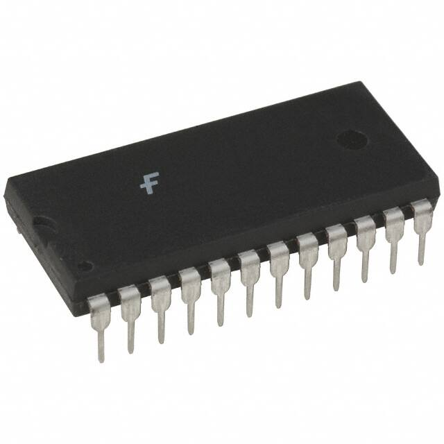


 工商网监
湘ICP备2023018690号
工商网监
湘ICP备2023018690号
