Revised March 2000
DM74LS126A
Quad 3-STATE Buffer
General Description
This device contains four independent gates each of which
performs a non-inverting buffer function. The outputs have
the 3-STATE feature. When enabled, the outputs exhibit
the low impedance characteristics of a standard LS output
with additional drive capability to permit the driving of bus
lines without external resistors. When disabled, both the
output transistors are turned OFF presenting a high-impedance state to the bus line. Thus the output will act neither
as a significant load nor as a driver. To minimize the possibility that two outputs will attempt to take a common bus to
opposite logic levels, the disable time is shorter than the
enable time of the outputs.
Ordering Code:
Order Number
Package Number
Package Description
DM74LS126AM
M14A
14-Lead Small Outline Integrated Circuit (SOIC), JEDEC MS-120, 0.150 Narrow
DM74LS126AN
N14A
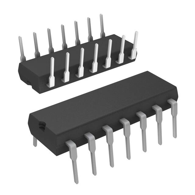
14-Lead Plastic Dual-In-Line Package (PDIP), JEDEC MS-001, 0.300 Wide
Devices also available in Tape and Reel. Specify by appending the suffix letter “X” to the ordering code.
Connection Diagram
Function Table
Y=A
Inputs
Output
A
C
L
H
Y
L
H
H
H
X
L
Hi-Z
H = HIGH Logic Level
L = LOW Logic Level
X = Either LOW or HIGH Logic Level
Hi-Z = 3-STATE (Outputs are disabled)
© 2000 Fairchild Semiconductor Corporation
DS006388
www.fairchildsemi.com
DM74LS126A Quad 3-STATE Buffer
August 1986
�DM74LS126A
Absolute Maximum Ratings(Note 1)
Supply Voltage
Note 1: The “Absolute Maximum Ratings” are those values beyond which
the safety of the device cannot be guaranteed. The device should not be
operated at these limits. The parametric values defined in the Electrical
Characteristics tables are not guaranteed at the absolute maximum ratings.
The “Recommended Operating Conditions” table will define the conditions
for actual device operation.
7V
Input Voltage
7V
0°C to +70°C
Operating Free Air Temperature Range
−65°C to +150°C
Storage Temperature Range
Recommended Operating Conditions
Symbol
Parameter
Min
Nom
Max
4.75
5
5.25
Units
VCC
Supply Voltage
VIH
HIGH Level Input Voltage
V
VIL
LOW Level Input Voltage
0.8
V
IOH
HIGH Level Output Current
−2.6
mA
IOL
LOW Level Output Current
24
mA
TA
Free Air Operating Temperature
70
°C
V
0
Electrical Characteristics
over recommended operating free air temperature range (unless otherwise noted)
Symbol
Parameter
Conditions
VI
Input Clamp Voltage
VCC = Min, II = −18 mA
VOH
HIGH Level
VCC = Min, IOH = Max
VOL
Output Voltage
VIH = Min
LOW Level
VCC = Min, IOL = Max
Output Voltage
VIL = Max, VIH = Min
Min
Typ
(Note 2)
Max
−1.5
2.4
IOL = 12 mA, VCC = Min
Units
V
V
0.35
0.5
0.25
0.4
V
II
Input Current @ Max Input Voltage
VCC = Max, VI = 7V
0.1
IIH
HIGH Level Input Current
VCC = Max, VI = 2.7V
20
µA
IIL
LOW Level Input Current
VCC = Max, VI = 0.4V
−0.4
mA
20
µA
−20
µA
IOZH
Off-State Output Current with
VCC = Max, VO = 2.4V
HIGH Level Output Voltage Applied
VIH = Min, VIL = Max
Off-State Output Current with
VCC = Max, VO = 0.4V
LOW Level Output Voltage Applied
VIH = Min, VIL = Max
IOS
Short Circuit Output Current
VCC = Max (Note 3)
ICC
Supply Current
VCC = Max
IOZL
−20
12
mA
−100
mA
22
mA
Note 2: All typicals are at VCC = 5V, TA = 25°C.
Note 3: Not more than one output should be shorted at a time, and the duration should not exceed one second.
Switching Characteristics
VCC = 5V, TA = 25°C
RL = 667Ω
Symbol
CL = 50 pF
Parameter
Min
Max
CL = 150 pF
Min
Units
Max
tPLH
Propagation Delay Time LOW-to-HIGH Level Output
15
21
ns
tPHL
Propagation Delay Time HIGH-to-LOW Level Output
18
22
ns
tPZH
Output Enable Time to HIGH Level Output
30
36
ns
tPZL
Output Enable Time to LOW Level Output
30
42
ns
tPHZ
Output Disable Time from HIGH Level Output (Note 4)
25
ns
tPLZ
Output Disable Time from LOW Level Output (Note 4)
25
ns
Note 4: CL = 5pF.
www.fairchildsemi.com
2
�DM74LS126A
Physical Dimensions inches (millimeters) unless otherwise noted
14-Lead Small Outline Integrated Circuit (SOIC), JEDEC MS-120, 0.150 Narrow
Package Number M14A
3
www.fairchildsemi.com
�DM74LS126A Quad 3-STATE Buffer
Physical Dimensions inches (millimeters) unless otherwise noted (Continued)
14-Lead Plastic Dual-In-Line Package (PDIP), JEDEC MS-001, 0.300 Wide
Package Number N14A
Fairchild does not assume any responsibility for use of any circuitry described, no circuit patent licenses are implied and
Fairchild reserves the right at any time without notice to change said circuitry and specifications.
LIFE SUPPORT POLICY
FAIRCHILD’S PRODUCTS ARE NOT AUTHORIZED FOR USE AS CRITICAL COMPONENTS IN LIFE SUPPORT
DEVICES OR SYSTEMS WITHOUT THE EXPRESS WRITTEN APPROVAL OF THE PRESIDENT OF FAIRCHILD
SEMICONDUCTOR CORPORATION. As used herein:
2. A critical component in any component of a life support
device or system whose failure to perform can be reasonably expected to cause the failure of the life support
device or system, or to affect its safety or effectiveness.
1. Life support devices or systems are devices or systems
which, (a) are intended for surgical implant into the
body, or (b) support or sustain life, and (c) whose failure
to perform when properly used in accordance with
instructions for use provided in the labeling, can be reasonably expected to result in a significant injury to the
user.
www.fairchildsemi.com
www.fairchildsemi.com
4
�
很抱歉,暂时无法提供与“DM74LS126AN”相匹配的价格&库存,您可以联系我们找货
免费人工找货