Revised April 2000
DM74S112
Dual Negative-Edge-Triggered Master-Slave J-K Flip-Flop
with Preset, Clear, and Complementary Outputs
General Description
This device contains two independent negative-edge-triggered J-K flip-flops with complementary outputs. The J and
K data is processed by the flip-flops on the falling edge of
the clock pulse. The clock triggering occurs at a voltage
level and is not directly related to the transition time of the
negative going edge of the clock pulse. Data on the J and
K inputs can be changed while the clock is HIGH or LOW
without affecting the outputs as long as setup and hold
times are not violated. A low logic level on the preset or
clear inputs will set or reset the outputs regardless of the
logic levels of the other inputs.
Ordering Code:
Order Number
DM74S112
Package Number
N16E
Package Description
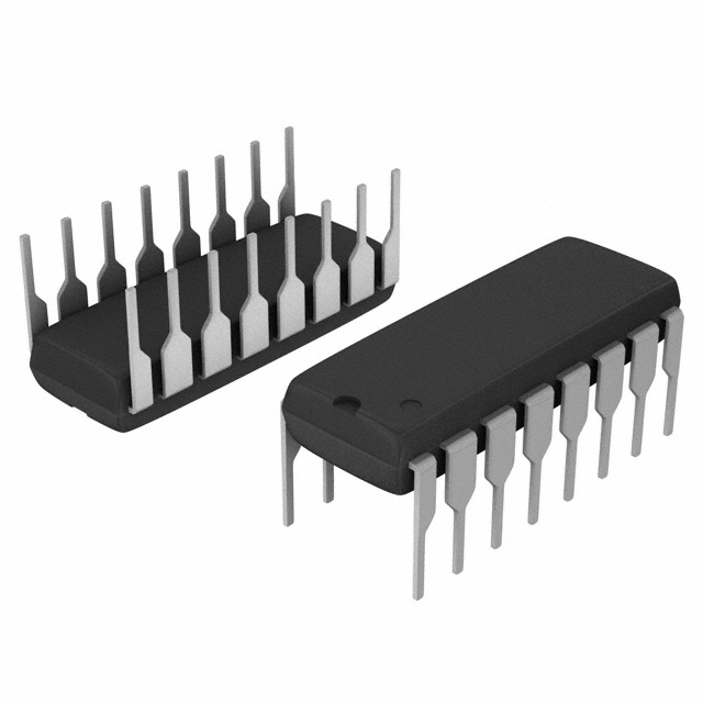
16-Lead Plastic Dual-In-Line Package (PDIP), JEDEC MS-001, 0.300 Wide
Connection Diagram
Function Table
Inputs
Outputs
PR
CLR
CLK
J
K
Q
L
H
X
X
X
H
Q
L
H
L
X
X
X
L
H
L
L
X
X
X
H*
H*
H
H
↓
L
L
Q0
Q0
H
H
↓
H
L
H
L
H
H
↓
L
H
L
H
H
H
↓
H
H
H
H
H
X
X
Toggle
Q0
Q0
H = HIGH Logic Level
X = Either LOW or HIGH Logic Level
L = LOW Logic Level
↓ = Negative going edge of pulse.
Q0 = The output logic level of Q before the indicated input conditions were
established.
* = This configuration is nonstable; that is, it will not persist when either the
preset and/or clear inputs return to its inactive (HIGH) level.
Toggle = Each output changes to the complement of its previous level on
each falling edge of the clock pulse.
© 2000 Fairchild Semiconductor Corporation
DS006459
www.fairchildsemi.com
DM74S112 Dual Negative-Edge-Triggered Master-Slave J-K Flip-Flop with Preset, Clear, and Complementary
Outputs
August 1986
�DM74S112
Absolute Maximum Ratings(Note 1)
Supply Voltage
Note 1: The “Absolute Maximum Ratings” are those values beyond which
the safety of the device cannot be guaranteed. The device should not be
operated at these limits. The parametric values defined in the Electrical
Characteristics tables are not guaranteed at the absolute maximum ratings.
The “Recommended Operating Conditions” table will define the conditions
for actual device operation.
7V
Input Voltage
5.5V
0°C to +70°C
Operating Free Air Temperature Range
−65°C to +150°C
Storage Temperature Range
Recommended Operating Conditions
Symbol
Parameter
Min
Nom
Max
Units
4.75
5
5.25
V
VCC
Supply Voltage
VIH
HIGH Level Input Voltage
VIL
LOW Level Input Voltage
0.8
V
IOH
HIGH Level Output Current
−1
mA
2
IOL
LOW Level Output Current
fCLK
Clock Frequency (Note 2)
fCLK
Clock Frequency (Note 3)
tW
Pulse Width
Clock HIGH
6
(Note 2)
Clock LOW
6.5
Clear LOW
8
Preset LOW
8
tW
20
mA
0
125
80
MHz
0
80
60
MHz
Pulse Width
Clock HIGH
8
(Note 3)
Clock LOW
8
Clear LOW
10
Preset LOW
10
tSU
Setup Time (Note 4)(Note 5)
7↓
tH
Input Hold Time (Note 4)(Note 5)
0↓
TA
Free Air Operating Temperature
0
Note 2: CL = 15 pF, R L = 280Ω, TA = 25°C and VCC = 5V.
Note 3: CL = 50 pF, R L = 280Ω, TA = 25°C and VCC = 5V.
Note 4: TA = 25°C and V CC = 5V.
Note 5: The symbol (↓) indicates the falling edge at the clock pulse is used for reference.
www.fairchildsemi.com
2
V
ns
ns
ns
ns
70
°C
�over recommended operating free air temperature (unless otherwise noted)
Symbol
Parameter
Conditions
VI
Input Clamp Voltage
VCC = Min, II = − 18 mA
VOH
HIGH Level
VCC = Min, IOH = Max
Output Voltage
VIL = Max, VIH = Min
LOW Level
VCC = Min, IOL = Max
Output Voltage
VIH = Min, VIL = Max
VOL
II
Input Current @ Max Input Voltage VCC = Max, VI = 5.5V
IIH
HIGH Level
VCC = Max
Input Current
VI = 2.7V
IIL
LOW Level
Input Current
Min
Typ
(Note 6)
2.7
Max
Units
−1.2
V
3.4
V
0.5
V
1
mA
J, K
50
Clear
100
Preset
100
Clock
100
VCC = Max
J, K
−1.6
VI = 0.5V
Clear
−7
(Note 7)
Preset
−7
Short Circuit Output Current
VCC = Max (Note 8)
ICC
Supply Current
VCC = Max (Note 9)
mA
−4
Clock
IOS
µA
−40
−100
mA
50
mA
30
Note 6: All typicals are at VCC = 5V, TA = 25°C.
Note 7: Clear is tested with preset HIGH and preset is tested with clear HIGH.
Note 8: Not more than one output should be shorted at a time, and the duration should not exceed one second.
Note 9: With all outputs OPEN, ICC is measured with the Q and Q outputs HIGH in turn. At the time of measurement, the clock input is grounded.
Switching Characteristics
at VCC = 5V and TA = 25°C
RL = 280Ω
Symbol
Parameter
CL = 15 pF
From (Input)
To (Output)
fMAX
Maximum Clock Frequency
tPLH
Propagation Delay Time
LOW-to-HIGH Level Output
tPHL
Propagation Delay Time
HIGH-to-LOW Level Output
tPLH
Propagation Delay Time
tPHL
Propagation Delay Time
LOW-to-HIGH Level Output
HIGH-to-LOW Level Output
tPLH
Propagation Delay Time
LOW-to-HIGH Level Output
tPHL
Propagation Delay Time
HIGH-to-LOW Level Output
Min
CL = 50 pF
Max
80
Min
Units
Max
60
MHz
Preset to Q
7
9
ns
Preset to Q
7
12
ns
Clear to Q
7
9
ns
Clear to Q
7
12
ns
Clock to Q or Q
7
9
ns
Clock to Q or Q
7
12
ns
3
www.fairchildsemi.com
DM74S112
Electrical Characteristics
�DM74S112 Dual Negative-Edge-Triggered Master-Slave J-K Flip-Flop with Preset, Clear, and Complementary
Outputs
Physical Dimensions inches (millimeters) unless otherwise noted
16-Lead Plastic Dual-In-Line Package (PDIP), JEDEC MS-001, 0.300 Wide
Package Number N16E
Fairchild does not assume any responsibility for use of any circuitry described, no circuit patent licenses are implied and
Fairchild reserves the right at any time without notice to change said circuitry and specifications.
LIFE SUPPORT POLICY
FAIRCHILD’S PRODUCTS ARE NOT AUTHORIZED FOR USE AS CRITICAL COMPONENTS IN LIFE SUPPORT
DEVICES OR SYSTEMS WITHOUT THE EXPRESS WRITTEN APPROVAL OF THE PRESIDENT OF FAIRCHILD
SEMICONDUCTOR CORPORATION. As used herein:
2. A critical component in any component of a life support
device or system whose failure to perform can be reasonably expected to cause the failure of the life support
device or system, or to affect its safety or effectiveness.
1. Life support devices or systems are devices or systems
which, (a) are intended for surgical implant into the
body, or (b) support or sustain life, and (c) whose failure
to perform when properly used in accordance with
instructions for use provided in the labeling, can be reasonably expected to result in a significant injury to the
user.
www.fairchildsemi.com
www.fairchildsemi.com
4
�
很抱歉,暂时无法提供与“DM74S112N”相匹配的价格&库存,您可以联系我们找货
免费人工找货