ECLLQFP32EVB
Evaluation Board User's
Manual for High Frequency
LQFP32
http://onsemi.com
EVAL BOARD USER’S MANUAL
INTRODUCTION
ON Semiconductor has developed an evaluation board
for the devices in 32−lead LQFP package. These evaluation
boards are offered as a convenience for the customers
interested in performing their own engineering assessment
on the general performance of the 32−lead LQFP device
samples. The board provides a high bandwidth 50 W
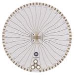
controlled impedance environment. Figures 1 and 2 show
the top and bottom view of the evaluation board, which can
be configured in several different ways, depending on
device under test (see Table 1. Configuration List).
This evaluation board manual contains:
•
•
•
•
This manual should be used in conjunction with the device
data sheet, which contains full technical details on the device
specifications and operation.
Board Lay−Up
The 32−lead LQFP evaluation board is implemented in
four layers with split (dual) power supplies (see Figure 3.
Evaluation Board Lay−Up). For standard ECL lab setup and
test, a split (dual) power supply is essential to enable the
50 W internal impedance in the oscilloscope as a termination
for ECL devices. The first layer or primary trace layer is
0.008″ thick Rogers RO4003 material, which is designed to
have equal electrical length on all signal traces from the
device under the test (DUT) to the sense output. The second
layer is the 1.0 oz copper ground. The FR4 dielectric
material is placed between second and third layer and
between third and fourth layer. The third layer is the power
plane (VCC and VEE) and a portion of this layer is a ground
plane. The fourth layer is the secondary trace layer.
Information on 32−lead LQFP Evaluation Board
Assembly Instructions
Appropriate Lab Setup
Bill of Materials
Figure 1. Top View of the 32−lead LQFP Evaluation Board
© Semiconductor Components Industries, LLC, 2012
January, 2012 − Rev. 3
1
Publication Order Number:
EVBUM2055/D
�ECLLQFP32EVB
Bottom View
Enlarged Bottom View
Figure 2. Bottom View of the 32−lead LQFP Evaluation Board
LAY−UP DETAIL
4 LAYER
SILKSCREEN (TOP SIDE)
LAYER 1 (TOP SIDE) 1 OZ
ROGERS 4003 0.008 in
LAYER 2 (GROUND PLANE P1) 1 OZ
FR−4 0.020 in
LAYER 3 (GROUND, VCC & VEE, PLANE P2) 1 OZ
FR−4 0.025 in
LAYER 4 (BOTTOM SIDE) 1 OZ
0.062 $ 0.007
Figure 3. Evaluation Board Lay−up
Board Layout
PCB board. Lists of components and simple schematics are
located in Figures 6 through 18. Place SMA connectors on
J1 through J32, 50 W chip resistors between ground pad and
Pin 1 pad through Pin 32 pad, and chip capacitors C1 through
C5 according to configuration figures. (C4 and C5 are 0.01
mF and C1, C2, and C3 are 0.1ĂmF); (See Figure 5).
The 32−lead LQFP evaluation board was designed to be
versatile and accommodate several different configurations.
The input, output, and power pin layout of the evaluation
board is shown in Figures 4 and 5. The evaluation board has
at least thirteen possible configurable options. Table 1, list
the devices and the relevant configuration that utilizes this
http://onsemi.com
2
�ECLLQFP32EVB
Top View
Bottom View
Figure 4. Evaluation Board Layout
http://onsemi.com
3
�Pin 32
Pin 31
Pin 30
Pin 29
Pin 28
Pin 27
Pin 26
Pin 25
ECLLQFP32EVB
VEE
VCC
C5
Ground
Pin 24
Pin 1
Pin 23
Pin 2
Pin 22
Pin 3
Pin 21
Pin 4
Pin 20
Pin 5
Pin 19
Pin 6
Pin 18
Pin 7
Pin 17
Pin 8
Pin 9
Pin 10
Pin 11
Pin 12
Pin 13
Pin 14
Pin 15
Pin 16
C4
Figure 5. Enlarged Bottom View of the Evaluation Board
Table 1. Configuration List
Configuration
Comments
Device
1
See Figure 6
LVE164
2
See Figure 7
EP016 / EP016A
3
See Figure 8
EP101 / EP105
4
See Figure 9
EP116
5
See Figure 10
EP131
6
See Figure 11
EP142
7
See Figure 12
EP195 / EP196
8
See Figure 13
EP445
9
See Figure 14
EP446
10
See Figure 15
EP451
11
See Figure 16
EP809
12
See Figure 17
LVEP111 / LVEP210
13
See Figure 18
LVEP210S
http://onsemi.com
4
�ECLLQFP32EVB
Evaluation Board Assembly Instructions
The 32−lead LQFP evaluation board is designed for
characterizing devices in a 50 W laboratory environment
using high bandwidth equipment. Each signal trace on the
board has a via, which has an option of placing a termination
resistor depending on the input/output configuration (see
Table 1, Configuration List). Table 17 contains the Bill of
Materials for this evaluation board.
It is recommended to solder 0.01 mF capacitors to C4 and
C5 to reduce the unwanted noise from the power supplies.
C1, C2, and C3 pads are provided for 0.1 mF capacitor to
further diminish the noise from the power supplies. Adding
capacitors can improve edge rates, reduce overshoot and
undershoot.
Termination
All ECL outputs need to be terminated to VTT (VTT = VCC
–2.0 V = GND) via a 50 W resistor. 0402 chip resistor pads
are provided on the bottom side of the evaluation board to
terminate the ECL driver (More information on termination
is provided in AN8020). Solder the chip resistors to the
bottom side of the board between the appropriate input of the
device pin pads and the ground pads. For ease of assembly,
it is advised to place and solder termination resistors on its
vertical (side) position, instead of its original or flat position.
Solder the Device on the Evaluation Board
The soldering can be accomplished by hand soldering or
soldering re−flow techniques. Make sure pin 1 of the device
is located next to the white dotted mark and all the pins are
aligned to the footprint pads. Solder the 32−lead LQFP
device to the evaluation board.
Connecting Power and Ground Planes
For standard ECL lab setup and test, a split (dual) power
supply is required enabling the 50 W internal impedance in
the oscilloscope to be used as a termination of the ECL
signals (VTT = VCC – 2.0 V, in split power supply setup, VTT
is the system ground, VCC is 2.0 V, and VEE is –3.0 V or
–1.3 V; see Table 2, Power Supply Levels).
Installing the SMA Connectors
Each configuration indicates the number of SMA
connectors needed to populate an evaluation board for a
given configuration. Each input and output requires one
SMA connector. Attach all the required SMA connectors
onto the board and solder the connectors to the board on J1
through J32. Please note that alignment of the signal
connector pin of the SMA can influence the lab results. The
reflection and launch of the signals are largely influenced by
imperfect alignment and soldering of the SMA connector.
Table 2. Power Supply Levels
Power Supply
VCC
VEE
GND
5.0 V
2.0 V
−3.0 V
0.0 V
3.3 V
2.0 V
−1.3 V
0.0 V
2.5 V
2.0 V
−0.5 V
0.0 V
Validating the Assembled Board
After assembling the evaluation board, it is recommended
to perform continuity checks on all soldered areas before
commencing with the evaluation process. Time Domain
Reflectometry (TDR) is another highly recommended
validation test.
Connect three banana jack sockets to VCC, VEE, and GND
labeled holes. Wire bond the appropriate device pin pad on
the bottom side of the board to VCC and VEE power stripes.
(Device specific, please see configuration for each desired
device. See Figure 5)
http://onsemi.com
5
�ECLLQFP32EVB
CONFIGURATIONS
SMA CONNECTORS
J31
J30 J29 J28 J27
J26
J2
J23
J3
J22
J4
J21
J5
J20
J6
J19
BANANA
JACK PLUG
0603 CHIP
CAPACITOR
0.1 mF
J9
J15
J10
J11
J13
J12
NORMAL TOP VIEW
LVE164
VEE
VCC
0805 CHIP
CAPACITOR
0.01 mF
PIN 1
0402 CHIP
RESISTOR
50 W
WIRE
EXPANDED BOTTOM VIEW
LVE164
Figure 6. Configuration 1
7
N Y
Y
Y
Y
Y N Y
N
N N
Y
Y
Y
Y N N Y
Y
Y
N Y Y Y
N N N N
Y
N
Y N
N Y
N Y Y
N N N
Y
N
N N N Y
N N Y N
N
N
N N
N Y
Y Y Y
N N N
Y
N
Y N N Y
N N N N
Y
N
Y Y
N N
J32
6
Y N
J31
5
Y
J30
J29
J28
J27
J26
J25
J24
J23
J22
J21
J20
J19
J18
J17
J16
J15
J14
J13
J12
J11
J10
4
Y
8
J9
J7
J8
J6
3
Y
Resistor
Power
J5
J2
2
Pin #
J4
J1
1
Connector N Y
Device
J3
Table 3. Configuration 1 (Device LVE164)
9 10 11 12 13 14 15 16 17 18 19 20 21 22 23 24 25 26 27 28 29 30 31 32
http://onsemi.com
6
Y
Y
Y
Y N
Y Y N
N N N
�ECLLQFP32EVB
SMA CONNECTORS
J31
J30 J29
J27
J26
J25
J24
J2
J23
J3
J22
J4
J21
J5
J20
J6
J19
J7
J18
BANANA
JACK PLUG
0603 CHIP
CAPACITOR
0.1 mF
J16
J15
J14
J10
J11
J17
J12
NORMAL TOP VIEW
EP016 / EP016A
VEE
VCC
0805 CHIP
CAPACITOR
0.01 mF
PIN 1
0402 CHIP
RESISTOR
50 W
WIRE
EXPANDED BOTTOM VIEW
EP016 / EP016A
Figure 7. Configuration 2
Y Y
N N
J32
Y
Y
N
J31
Y
J30
Y
N N Y Y
N Y N N
J29
Y N Y
N
N
J28
Y
N N N
Y Y N
J27
N N Y
J26
Y
J25
Y
N Y
N N
J24
Y
N
N
J23
8
J22
7
J21
6
J20
5
J19
J18
J17
J16
J15
J14
J13
J12
Y
J11
Y
N N N N
Y N N N
Resistor
Power
J10
Connector N Y
J9
4
J8
J4
3
J7
J3
2
Pin #
J6
J2
1
Device
J5
J1
Table 4. Configuration 2 (Device EP016 and EP016A)
9 10 11 12 13 14 15 16 17 18 19 20 21 22 23 24 25 26 27 28 29 30 31 32
http://onsemi.com
7
Y
Y
Y
Y
Y
Y
Y
N Y
Y
Y Y Y
N N N
Y
Y
N
Y N Y Y
N N N N
Y
Y
Y
N
N N
Y N
N N N
N N Y
Y N
�ECLLQFP32EVB
SMA CONNECTORS
J30 J29
J27
J26
J25
J24
J2
J23
J3
J22
J4
J21
J5
J20
J6
J19
J7
J18
BANANA
JACK PLUG
J11
0603 CHIP
CAPACITOR
0.1 mF
J17
J16
J15
J14
J12
NORMAL TOP VIEW
EP101 / EP105
VEE
VCC
0805 CHIP
CAPACITOR
0.01 mF
PIN 1
0402 CHIP
RESISTOR
50 W
WIRE
EXPANDED BOTTOM VIEW
EP101 / EP105
Figure 8. Configuration 3
Y Y
N N
J32
Y
Y
N
J31
Y
J30
Y
Y N Y Y
N Y N N
J29
Y N Y
Y
N
J28
Y
N N N
Y N Y
J27
N N N
J26
Y
J25
Y
N N
N N
J24
Y
N
N
J23
8
J22
7
J21
6
J20
5
J19
J18
J17
J16
J15
J14
J13
J12
Y
J11
Y
N N N N
Y N N N
Resistor
Power
J10
Connector N Y
J9
4
J8
J4
3
J7
J3
2
Pin #
J6
J2
1
Device
J5
J1
Table 5. Configuration 3 (Device EP101 and EP105)
9 10 11 12 13 14 15 16 17 18 19 20 21 22 23 24 25 26 27 28 29 30 31 32
http://onsemi.com
8
Y
Y
Y
Y
Y
Y
Y
N Y
Y N N
Y Y Y
N N N
Y
Y
N
Y Y Y Y
N N N N
Y
Y
Y
N
N N
Y N
N N N
N Y Y
�ECLLQFP32EVB
SMA CONNECTORS
J32
J31
J30 J29
J27
J26
J1
J25
J24
J2
J23
J3
J22
J4
J21
J5
J20
J6
J19
J7
J18
BANANA
JACK PLUG
0603 CHIP
CAPACITOR
0.1 mF
J15
J14
J10
J11
NORMAL TOP VIEW
EP116
VEE
VCC
0805 CHIP
CAPACITOR
0.01 mF
PIN 1
0402 CHIP
RESISTOR
50 W
WIRE
EXPANDED BOTTOM VIEW
EP116
Figure 9. Configuration 4
J32
J31
J30
J29
J28
J27
J26
J25
J24
J23
J22
J21
J20
J19
J18
J17
J16
J15
J14
Y
J13
Y
J12
Y
Y Y N N
N N N N
Resistor
Power
J11
Connector Y
J10
4
J9
3
J8
J4
2
J7
J3
1
J6
J2
Pin #
J5
Device
J1
Table 6. Configuration 4 (Device EP116)
5
6
7
8
Y
Y
Y
N N Y
Y
N N Y
Y
N
N Y
Y
Y
Y
Y
Y
Y
N Y
Y
N
N
N N
N N
N N N
Y Y N
N
N
N N N N
Y Y N N
N
Y
N N
Y N
N N N
N N N
Y
N
Y Y Y Y
N N N N
Y
N
N Y
Y N
Y Y Y
N N N
9 10 11 12 13 14 15 16 17 18 19 20 21 22 23 24 25 26 27 28 29 30 31 32
http://onsemi.com
9
Y
Y
Y
Y
Y
�ECLLQFP32EVB
SMA CONNECTORS
J32
J31
J30 J29
J27
J26
J1
J24
J2
J23
J3
J22
J4
J21
J5
J20
J6
J19
J7
J18
BANANA
JACK PLUG
J8
0603 CHIP
CAPACITOR
0.1 mF
J15
J14
J10
J11
J17
J12
NORMAL TOP VIEW
EP131
VEE
VCC
0805 CHIP
CAPACITOR
0.01 mF
PIN 1
0402 CHIP
RESISTOR
50 W
WIRE
EXPANDED BOTTOM VIEW
EP131
Figure 10. Configuration 5
Y
Y
Y
Y N Y
Y
Y N Y
Y
N
Y
Y
N
Y Y
N N
Y N Y
N Y N
Y
N
Y N Y Y
N Y N N
N
Y
N N
N N
J32
Y
J31
Y
J30
Y
Y Y Y Y
N N N N
J29
Connector Y
J28
8
J27
7
J26
6
J25
5
J24
4
J23
3
J22
2
J21
1
J20
Pin #
J19
J18
J8
J17
J7
J16
J6
J15
J5
J14
J4
J13
J3
J12
J2
J11
J1
J10
Device
Resistor
Power
J9
Table 7. Configuration 5 (Device EP131)
9 10 11 12 13 14 15 16 17 18 19 20 21 22 23 24 25 26 27 28 29 30 31 32
http://onsemi.com
10
Y
Y
Y
Y
Y N Y
Y
N Y
Y
N N N
N N N
Y
Y
N
N
N N N Y
N N Y N
Y
N
N Y
Y N
Y Y Y
N N N
Y
Y
�ECLLQFP32EVB
SMA CONNECTORS
J31
J30 J29
J27
J26
J1
J25
J24
J2
J23
J3
J22
J4
J21
J5
J20
J6
J19
J7
J18
BANANA
JACK PLUG
J8
0603 CHIP
CAPACITOR
0.1 mF
J9
J15
J14
J10
J11
J12
NORMAL TOP VIEW
EP142
VEE
VCC
0805 CHIP
CAPACITOR
0.01 mF
PIN 1
0402 CHIP
RESISTOR
50 W
WIRE
EXPANDED BOTTOM VIEW
EP142
Figure 11. Configuration 6
J32
J31
J30
J29
J28
J27
J26
J25
J24
J23
J22
J21
J20
J19
J18
J8
J17
J7
J16
J6
J15
J5
J14
J4
J13
J3
J12
J2
J11
J1
J10
Device
Pin #
1
2
3
4
5
6
7
8
9 10 11 12 13 14 15 16 17 18 19 20 21 22 23 24 25 26 27 28 29 30 31 32
Connector Y
Y
Y
Y
Y
Y
Y
Y
Y
Y Y Y Y
N N N N
Y
N
Y Y
N N
Resistor
Power
J9
Table 8. Configuration 6 (Device EP142)
Y
Y
Y N N N
N
N Y
Y
Y
Y
Y
Y
Y
N Y
Y
Y Y N
N N N
N
N
N N N N
N Y Y Y
N
Y
N N
Y N
N N N
N N N
N
N
Y Y Y Y
N N N N
Y
N
N Y
Y N
Y Y N
N N Y
http://onsemi.com
11
Y
Y
Y
Y N
�ECLLQFP32EVB
SMA CONNECTORS
J32
J31
J30 J29
J27
J26
J25
J1
J2
J23
J3
J4
J21
J5
J20
J7
BANANA
JACK PLUG
J8
0603 CHIP
CAPACITOR
0.1 mF
J16
J15
J14
J10
J11
J17
J12
Only for EP196
NORMAL TOP VIEW
EP195 / EP196
VEE
VCC
0805 CHIP
CAPACITOR
0.01 mF
PIN 1
0402 CHIP
RESISTOR
50 W
WIRE
EXPANDED BOTTOM VIEW
EP195 / EP196
Figure 12. Configuration 7
N N
N Y
J32
*
Y
N
J31
Y
J30
Y N Y
Y Y N Y
N N Y N
J29
Y
Y
N
J28
Y
J27
Y N Y
N N Y
N Y N
J26
Y
N N
N N
J25
Y
Y
N
J24
Y
J23
8
J22
7
J21
6
J20
5
J19
J18
J17
J16
J15
J14
Y
J13
Y
J12
Y
Y Y Y Y
Resistor
N N N N
Power
* Only for EP196
J11
Connector Y
J10
4
J9
3
J8
J4
2
J7
J3
1
J6
J2
Pin #
J5
Device
J1
Table 9. Configuration 7 (Device EP195 and EP196)
9 10 11 12 13 14 15 16 17 18 19 20 21 22 23 24 25 26 27 28 29 30 31 32
http://onsemi.com
12
N
N Y
Y
N
Y N Y
Y
Y
N Y
Y
N N N
Y N N
N
Y
Y N Y Y
N Y N N
Y
N
N Y
Y N
Y Y Y
N N N
Y
Y
�ECLLQFP32EVB
SMA CONNECTORS
J31
J30 J29
J27
J26
J25
J1
J2
J23
J3
J22
J4
J21
J5
J6
J19
J7
J18
BANANA
JACK PLUG
0603 CHIP
CAPACITOR
0.1 mF
J9
J15
J14
J10
J11
NORMAL TOP VIEW
EP445
VEE
VCC
0805 CHIP
CAPACITOR
0.01 mF
PIN 1
0402 CHIP
RESISTOR
50 W
WIRE
EXPANDED BOTTOM VIEW
EP445
Figure 13. Configuration 8
J32
J31
J30
J29
J28
J27
J26
J25
J24
J23
J22
J21
J20
J19
J18
J17
Y
N Y
N N
J16
Y
Y
N
J15
Y
J14
Y
J13
Y
J12
Y
Y Y Y Y
N N N N
Resistor
Power
6
J11
Connector Y
5
J10
4
J9
3
J8
J4
2
J7
J3
1
J6
J2
Pin #
J5
Device
J1
Table 10. Configuration 8 (Device EP445)
7
8
9 10 11 12 13 14 15 16 17 18 19 20 21 22 23 24 25 26 27 28 29 30 31 32
Y
Y
Y
Y
N N Y
Y
N
N Y
Y N Y
Y
Y N Y
Y
Y
N Y
Y
N N N
N N N
N
N
N N N N
Y Y N N
N
Y
N N
Y N
N N N
N Y N
Y
N
Y N Y Y
N Y N N
Y
N
N N
Y N
Y Y N
N N Y
http://onsemi.com
13
Y N
�ECLLQFP32EVB
SMA CONNECTORS
J31
J30 J29
J27
J26
J24
J2
J23
J3
J22
J4
J21
J5
J20
J6
J19
J7
J18
BANANA
JACK PLUG
J11
0603 CHIP
CAPACITOR
0.1 mF
J17
J15
J14
J12
NORMAL TOP VIEW
EP446
VEE
VCC
0805 CHIP
CAPACITOR
0.01 mF
PIN 1
0402 CHIP
RESISTOR
50 W
WIRE
EXPANDED BOTTOM VIEW
EP446
Figure 14. Configuration 9
N
Y
N
Y
Y Y
N N
J32
Y
N N N N
N Y N N
J31
Y N Y
N
N
J30
Y
N N N
Y Y Y
J29
N N N
J28
Y
Y Y
N N
J27
Y
J26
Y
N
N
J25
Y
N Y Y Y
Y N N N
J24
8
J23
7
J22
6
J21
5
J20
4
J19
J18
J17
J16
J15
J14
J13
J12
J11
Y
J10
J8
Connector N Y
J9
J7
3
Resistor
Power
J6
J3
2
Pin #
J5
J2
1
Device
J4
J1
Table 11. Configuration 9 (Device EP446)
9 10 11 12 13 14 15 16 17 18 19 20 21 22 23 24 25 26 27 28 29 30 31 32
http://onsemi.com
14
Y
Y
Y
Y
Y
Y N Y
Y
N Y
Y
Y Y Y
N N N
Y
Y
N
Y Y N N
N N Y N
N
N
N Y
Y N
Y N N
N N Y
Y N
�ECLLQFP32EVB
SMA CONNECTORS
J32
J31
J30 J29
J27
J26
J1
J25
J24
J2
J23
J3
J22
J4
J21
J5
J20
J7
J18
BANANA
JACK PLUG
J8
0603 CHIP
CAPACITOR
0.1 mF
J9
J15
J14
J10
J11
J17
J12
NORMAL TOP VIEW
EP451
VEE
VCC
0805 CHIP
CAPACITOR
0.01 mF
PIN 1
0402 CHIP
RESISTOR
50 W
WIRE
EXPANDED BOTTOM VIEW
EP451
Figure 15. Configuration 10
J32
J31
J30
J29
J28
J27
J26
J25
J24
J23
J22
J21
Y
N
J20
Y
J19
Y
J18
Y
J17
Y
Y Y Y Y
N N N N
J16
Connector Y
J15
6
J14
5
J13
4
J12
J6
3
J11
J5
2
J10
J4
1
J9
J3
J8
J2
Pin #
Resistor
Power
J7
Device
J1
Table 12. Configuration 10 (Device EP451)
7
8
9 10 11 12 13 14 15 16 17 18 19 20 21 22 23 24 25 26 27 28 29 30 31 32
N Y
Y
Y
Y
Y
Y N Y
Y
N
Y
N N
Y N
N N N
N N N
N
N
N N N N
N Y N N
N
Y
N N
N N
http://onsemi.com
15
Y
N Y
Y
Y
Y
Y
Y
N Y
Y
N N N
Y N N
Y
N
Y Y Y Y
N N N N
Y
Y
Y
N
N Y
Y N
Y Y Y
N N N
Y
Y
�ECLLQFP32EVB
SMA CONNECTORS
J31
J30 J29 J28 J27
J26
J2
J23
J3
J22
J4
J21
J5
J20
J6
J19
J18
BANANA
JACK PLUG
J8
0603 CHIP
CAPACITOR
0.1 mF
J10
J11
J13
J12
J15
J14
NORMAL TOP VIEW
EP809
VEE = VCCO
VCC
0805 CHIP
CAPACITOR
0.01 mF
PIN 1
0402 CHIP
RESISTOR
50 W
WIRE
EXPANDED BOTTOM VIEW
EP809
Figure 16. Configuration 11
4
5
6
7
8
Connector N Y
Y
Y
Y
Y N
Y N Y
Y
Y
Y
N
N Y
Y
Y
Y
Y N N Y
Y
Y
N Y Y Y
Y N N N
Y
N
Y N
N Y
Y N N
N Y N
N
N
N N N N
N N N N
N
Y
N N
Y N
N N N
N N N
N
N
N N N N
N Y Y N
N
N
N N
N N
Resistor
Power
J32
3
J31
2
Pin #
J30
J29
J28
J27
J26
J25
J24
J23
J22
J21
J20
J19
J18
J17
J8
J16
J7
J15
J6
J14
J5
J13
J4
J12
J3
J11
J2
J10
J1
1
Device
J9
Table 13. Configuration 11 (Device EP809)
9 10 11 12 13 14 15 16 17 18 19 20 21 22 23 24 25 26 27 28 29 30 31 32
Y
Y
http://onsemi.com
16
Y
Y
Y
Y N
N N N
N N Y
�ECLLQFP32EVB
SMA CONNECTORS
J31
J30 J29 J28 J27
J26
J24
J2
J23
J3
J22
J4
J21
J20
J6
J19
J7
J18
BANANA
JACK PLUG
0603 CHIP
CAPACITOR
0.1 mF
J10
J11
J13
J12
J17
J15
J14
NORMAL TOP VIEW
LVEP111 / LVEP210
VEE
VCC
0805 CHIP
CAPACITOR
0.01 mF
PIN 1
0402 CHIP
RESISTOR
50 W
WIRE
EXPANDED BOTTOM VIEW
LVEP111 / LVEP210
Figure 17. Configuration 12
N N Y
Y
Y
Y
N
Y
N N N
Y Y N
N
N
N N N N
N N N N
N
Y
N N
N N
J32
Y
J31
Y
J30
Y
J29
Y
J28
Y
N Y Y Y N Y Y
Resistor
Y N N N N N N
Power
* Pin 2 is No Connect for LVEP210
J27
Connector N Y
J26
8
J25
7
J24
6
J23
5
J22
4
J21
3
J20
2
Pin #
J19
J18
J17
J8
J16
J7
J15
J6
J14
J5
J13
J4
J12
J3
J11
J2
J10
J1
1
Device
J9
Table 14. Configuration 12 (Device LVEP111 and LVEP210)
9 10 11 12 13 14 15 16 17 18 19 20 21 22 23 24 25 26 27 28 29 30 31 32
Y
Y
http://onsemi.com
17
Y
Y
Y
Y
Y N Y
Y
Y
N N N
N N N
Y
Y
N
N
N N N N
N N Y N
N
N
N N
N N
Y
Y
Y N
N N N
N N Y
�ECLLQFP32EVB
SMA CONNECTORS
J31
J30 J29 J28 J27
J26
J24
J2
J23
J3
J22
J4
J21
J20
J6
J19
J7
J18
BANANA
JACK PLUG
0603 CHIP
CAPACITOR
0.1 mF
J10
J11
J13
J12
J17
J15
J14
NORMAL TOP VIEW
LVEP210S
VEE
VCC
0805 CHIP
CAPACITOR
0.01 mF
PIN 1
0402 CHIP
RESISTOR
50 W
WIRE
EXPANDED BOTTOM VIEW
LVEP210S
Figure 18. Configuration 13
N N Y
Y
Y
Y
N
Y
N N N
Y Y N
N
N
N N N N
N N N N
N
Y
N N
N N
J32
Y
Y Y
N N
J31
Y
Y
N
J30
Y
J29
Y
J28
Y
N Y Y Y
Y N N N
Resistor
Power
J27
Connector N Y
J26
8
J25
7
J24
6
J23
5
J22
4
J21
3
J20
2
Pin #
J19
J18
J17
J8
J16
J7
J15
J6
J14
J5
J13
J4
J12
J3
J11
J2
J10
J1
1
Device
J9
Table 15. Configuration 13 (Device LVEP210S)
9 10 11 12 13 14 15 16 17 18 19 20 21 22 23 24 25 26 27 28 29 30 31 32
Y
Y
http://onsemi.com
18
Y
Y
Y
Y
Y N Y
Y
Y
N N N
N N N
Y
Y
N
N
N N N N
N N Y N
N
N
N N
N N
Y
Y
Y N
N N N
N N Y
�ECLLQFP32EVB
LAB SETUP
Differential
Signal
Generator
Test Measuring
Equipment
J31
J30
J29
Out1
Out1
J28
J3
D
U
T
J4
J27
J26
J24
J23
Trigger
Channel 1
Channel 2
Channel 3
Channel 4
Channel 5
Channel 6
Channel 7
Channel 8
Trigger
VCC GND VEE
Power Supply
Figure 19. Example of Standard Lab Setup (Configuration 12)
1. Connect appropriate power supplies to VCC, VEE,
and GND.
For standard ECL lab setup and test, a split (dual)
power supply is required enabling the 50 W
internal impedance in the oscilloscope to be used
as a termination of the ECL signals (VTT = VCC
– 2.0 V, in split power supply setup, VTT is the
system ground, VCC is 2.0 V, and VEE is –3.0 V or
–1.3 V; see Table 16).
2. Connect a signal generator to the input SMA
connectors. Setup input signal according to the
device data sheet.
3. Connect a test measurement device on the device
output SMA connectors.
NOTE: The test measurement device must contain 50 W
termination.
Table 16. Power Supply Levels
Power Supply
VCC
VEE
GND
5.0 V
2.0 V
−3.0 V
0.0 V
3.3 V
2.0 V
−1.3 V
0.0 V
2.5 V
2.0 V
−0.5 V
0.0 V
Table 17. Bill of Materials
Components
Manufacturer
SMA Connector
Johnson
Components*
Banana Jack
Chip Capacitor
Chip Resistor
Keystone*
Johanson
Dielectric*
Panasonic*
Description
SMA Connector, Side Launch,
Gold Plated
Part Number
Web Site
142−0701−851
http://www.johnsoncomponents.com
Standard Jack
6096
Miniature Jack
6090
0603/0805/1205 0.01 mF
Chip Capacitor
−
0603/0805/1205 0.1 mF
Chip Capacitor
−
http://www.keyelco.com
http://www.johansondielectrics.com
0402 50 W ±1% Precision Think
Film Chip Resistor
ERJ−2RKF49R9X
http://www.panasonic.com
Evaluation Board
ON Semiconductor
LQFP32 Evaluation Board
ECLLQFP32EVB
http://www.onsemi.com
Device Samples
ON Semiconductor
LQFP32 Package Device
Various
http://www.onsemi.com
*Components are available through most distributors, i.e. www.newark.com, www.digikey.com.
http://onsemi.com
19
�ECLLQFP32EVB
Top View
Second Layer (Ground Plane)
Figure 20. Gerber Files
http://onsemi.com
20
�ECLLQFP32EVB
Third Layer (Power and Ground Plane)
(Left side − VCC, Right side − VEE, Middle Box − Ground)
Bottom Layer
Figure 21. Gerber Files
http://onsemi.com
21
�onsemi,
, and other names, marks, and brands are registered and/or common law trademarks of Semiconductor Components Industries, LLC dba “onsemi” or its affiliates
and/or subsidiaries in the United States and/or other countries. onsemi owns the rights to a number of patents, trademarks, copyrights, trade secrets, and other intellectual property. A
listing of onsemi’s product/patent coverage may be accessed at www.onsemi.com/site/pdf/Patent−Marking.pdf. onsemi is an Equal Opportunity/Affirmative Action Employer. This
literature is subject to all applicable copyright laws and is not for resale in any manner.
The evaluation board/kit (research and development board/kit) (hereinafter the “board”) is not a finished product and is not available for sale to consumers. The board is only intended
for research, development, demonstration and evaluation purposes and will only be used in laboratory/development areas by persons with an engineering/technical training and familiar
with the risks associated with handling electrical/mechanical components, systems and subsystems. This person assumes full responsibility/liability for proper and safe handling. Any
other use, resale or redistribution for any other purpose is strictly prohibited.
THE BOARD IS PROVIDED BY ONSEMI TO YOU “AS IS” AND WITHOUT ANY REPRESENTATIONS OR WARRANTIES WHATSOEVER. WITHOUT LIMITING THE FOREGOING,
ONSEMI (AND ITS LICENSORS/SUPPLIERS) HEREBY DISCLAIMS ANY AND ALL REPRESENTATIONS AND WARRANTIES IN RELATION TO THE BOARD, ANY
MODIFICATIONS, OR THIS AGREEMENT, WHETHER EXPRESS, IMPLIED, STATUTORY OR OTHERWISE, INCLUDING WITHOUT LIMITATION ANY AND ALL
REPRESENTATIONS AND WARRANTIES OF MERCHANTABILITY, FITNESS FOR A PARTICULAR PURPOSE, TITLE, NON−INFRINGEMENT, AND THOSE ARISING FROM A
COURSE OF DEALING, TRADE USAGE, TRADE CUSTOM OR TRADE PRACTICE.
onsemi reserves the right to make changes without further notice to any board.
You are responsible for determining whether the board will be suitable for your intended use or application or will achieve your intended results. Prior to using or distributing any systems
that have been evaluated, designed or tested using the board, you agree to test and validate your design to confirm the functionality for your application. Any technical, applications or
design information or advice, quality characterization, reliability data or other services provided by onsemi shall not constitute any representation or warranty by onsemi, and no additional
obligations or liabilities shall arise from onsemi having provided such information or services.
onsemi products including the boards are not designed, intended, or authorized for use in life support systems, or any FDA Class 3 medical devices or medical devices with a similar
or equivalent classification in a foreign jurisdiction, or any devices intended for implantation in the human body. You agree to indemnify, defend and hold harmless onsemi, its directors,
officers, employees, representatives, agents, subsidiaries, affiliates, distributors, and assigns, against any and all liabilities, losses, costs, damages, judgments, and expenses, arising
out of any claim, demand, investigation, lawsuit, regulatory action or cause of action arising out of or associated with any unauthorized use, even if such claim alleges that onsemi was
negligent regarding the design or manufacture of any products and/or the board.
This evaluation board/kit does not fall within the scope of the European Union directives regarding electromagnetic compatibility, restricted substances (RoHS), recycling (WEEE), FCC,
CE or UL, and may not meet the technical requirements of these or other related directives.
FCC WARNING – This evaluation board/kit is intended for use for engineering development, demonstration, or evaluation purposes only and is not considered by onsemi to be a finished
end product fit for general consumer use. It may generate, use, or radiate radio frequency energy and has not been tested for compliance with the limits of computing devices pursuant
to part 15 of FCC rules, which are designed to provide reasonable protection against radio frequency interference. Operation of this equipment may cause interference with radio
communications, in which case the user shall be responsible, at its expense, to take whatever measures may be required to correct this interference.
onsemi does not convey any license under its patent rights nor the rights of others.
LIMITATIONS OF LIABILITY: onsemi shall not be liable for any special, consequential, incidental, indirect or punitive damages, including, but not limited to the costs of requalification,
delay, loss of profits or goodwill, arising out of or in connection with the board, even if onsemi is advised of the possibility of such damages. In no event shall onsemi’s aggregate liability
from any obligation arising out of or in connection with the board, under any theory of liability, exceed the purchase price paid for the board, if any.
The board is provided to you subject to the license and other terms per onsemi’s standard terms and conditions of sale. For more information and documentation, please visit
www.onsemi.com.
PUBLICATION ORDERING INFORMATION
LITERATURE FULFILLMENT:
Email Requests to: orderlit@onsemi.com
onsemi Website: www.onsemi.com
◊
TECHNICAL SUPPORT
North American Technical Support:
Voice Mail: 1 800−282−9855 Toll Free USA/Canada
Phone: 011 421 33 790 2910
www.onsemi.com
1
Europe, Middle East and Africa Technical Support:
Phone: 00421 33 790 2910
For additional information, please contact your local Sales Representative
�


 工商网监
湘ICP备2023018690号
工商网监
湘ICP备2023018690号
