EMG2DXV5, EMG5DXV5
Dual Bias Resistor
Transistors
NPN Silicon Surface Mount Transistors
with Monolithic Bias Resistor Network
This new series of digital transistors is designed to replace a single
device and its external resistor bias network. The BRT (Bias Resistor
Transistor) contains a single transistor with a monolithic bias network
consisting of two resistors; a series base resistor and a base−emitter
resistor. The BRT eliminates these individual components by
integrating them into a single device. The use of a BRT can reduce
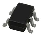
both system cost and board space. The device is housed in the
SOT−553 package which is designed for low power surface mount
applications.
http://onsemi.com
NPN SILICON
BIAS RESISTOR
TRANSISTORS
(5)
(4)
Q1
Q2
Features
•
•
•
•
•
•
•
Simplifies Circuit Design
Reduces Board Space
Reduces Component Count
Moisture Sensitivity Level: 1
Available in 8 mm, 7 inch Tape and Reel
Lead−Free Solder Plating
These Devices are Pb−Free, Halogen Free/BFR Free and are RoHS
Compliant
MAXIMUM RATINGS (TA = 25°C unless otherwise noted)
Rating
Symbol
Value
Unit
VCBO
50
Vdc
Collector-Emitter Voltage
VCEO
50
Vdc
IC
100
mAdc
Symbol
Max
Unit
Total Device Dissipation
TA = 25°C
Derate above 25°C
PD
230 (Note 1)
338 (Note 2)
1.8 (Note 1)
2.7 (Note 2)
mW
Thermal Resistance −
Junction-to-Ambient
RqJA
540 (Note 1)
370 (Note 2)
°C/W
Thermal Resistance −
Junction-to-Lead
RqJL
264 (Note 1)
287 (Note 2)
°C/W
Junction and Storage
Temperature Range
TJ, Tstg
−55 to +150
°C
THERMAL CHARACTERISTICS
Characteristic
March, 2013 − Rev. 1
R1
R1
(1)
(2)
(3)
SOT−553
CASE 463B
1
MARKING
DIAGRAM
5
XXM G
G
°C/W
1
Stresses exceeding Maximum Ratings may damage the device. Maximum
Ratings are stress ratings only. Functional operation above the Recommended
Operating Conditions is not implied. Extended exposure to stresses above the
Recommended Operating Conditions may affect device reliability.
1. FR−4 @ Minimum Pad
2. FR−4 @ 1.0 x 1.0 inch Pad
© Semiconductor Components Industries, LLC, 2013
R2
5
Collector-Base Voltage
Collector Current
R2
1
XX = UF (EMG5)
UP (EMG2)
M = Date Code
G = Pb−Free Package
(Note: Microdot may be in either location)
ORDERING INFORMATION
See detailed ordering and shipping information in the package
dimensions section on page 6 of this data sheet.
Publication Order Number:
EMG5DXV5/D
�EMG2DXV5, EMG5DXV5
DEVICE MARKING AND RESISTOR VALUES
Package
Marking
R1 (K)
R2 (K)
EMG2DXV5
Device
SOT−553
UP
47
47
EMG5DXV5
SOT−553
UF
10
47
ELECTRICAL CHARACTERISTICS (TA = 25°C unless otherwise noted)
Characteristic
Symbol
Min
Typ
Max
Unit
Collector-Base Cutoff Current (VCB = 50 V, IE = 0)
ICBO
−
−
100
nAdc
Collector-Emitter Cutoff Current (VCE = 50 V, IB = 0)
ICEO
−
−
500
nAdc
Emitter-Base Cutoff Current (VEB = 6.0 V, IC = 0)
IEBO
−
−
−
−
0.1
0.2
mAdc
Collector-Base Breakdown Voltage (IC = 10 mA, IE = 0)
V(BR)CBO
50
−
−
Vdc
Collector-Emitter Breakdown Voltage (Note 3)
(IC = 2.0 mA, IB = 0)
V(BR)CEO
50
−
−
Vdc
hFE
80
80
140
140
−
−
VCE(sat)
−
−
0.25
−
−
−
−
0.2
0.2
VOH
4.9
−
−
Vdc
kW
OFF CHARACTERISTICS (Q1 & Q2)
EMG2DXV5
EMG5DXV5
ON CHARACTERISTICS (Q1 & Q2) (Note 3)
DC Current Gain (VCE = 10 V, IC = 5.0 mA)
EMG2DXV5
EMG5DXV5
Collector-Emitter Saturation Voltage (IC = 10 mA, IB = 0.3 mA)
Output Voltage (on)
(VCC = 5.0 V, VB = 3.5 V, RL = 1.0 kW)
(VCC = 5.0 V, VB = 2.5 V, RL = 1.0 kW)
VOL
EMG2DXV5
EMG5DXV5
Output Voltage (off) (VCC = 5.0 V, VB = 0.5 V, RL = 1.0 kW)
Input Resistor
EMG2DXV5
EMG5DXV5
R1
32.9
7.0
47
10
61.1
13
Resistor Ratio
EMG2DXV5
EMG5DXV5
R1/R2
0.8
0.17
1.0
0.21
1.2
0.25
3. Pulse Test: Pulse Width < 300 ms, Duty Cycle < 2.0%
PD, POWER DISSIPATION (mW)
350
300
250
200
150
100
50
0
−50
RqJA = 370°C/W
0
50
100
TA, AMBIENT TEMPERATURE (°C)
Figure 1. Derating Curve
http://onsemi.com
2
150
Vdc
Vdc
�EMG2DXV5, EMG5DXV5
10
1000
hFE , DC CURRENT GAIN (NORMALIZED)
VCE(sat) , MAXIMUM COLLECTOR VOLTAGE (VOLTS)
TYPICAL ELECTRICAL CHARACTERISTICS — EMG2DXV5
IC/IB = 10
1
25°C
TA�=�-25°C
75°C
0.1
VCE = 10 V
TA�=�75°C
25°C
-25°C
100
0.01
0
10
50
20
40
IC, COLLECTOR CURRENT (mA)
10
IC, COLLECTOR CURRENT (mA)
1
Figure 2. VCE(sat) versus IC
Figure 3. DC Current Gain
1
100
f = 1 MHz
IE = 0 V
TA = 25°C
IC, COLLECTOR CURRENT (mA)
0.4
TA�=�-25°C
10
1
0.1
0.01
0.2
0
25°C
75°C
0.6
0
VO = 5 V
0.001
50
10
20
30
40
VR, REVERSE BIAS VOLTAGE (VOLTS)
0
Figure 4. Output Capacitance
2
4
6
Vin, INPUT VOLTAGE (VOLTS)
VO = 0.2 V
TA�=�-25°C
10
25°C
75°C
1
0.1
0
10
8
Figure 5. Output Current versus Input Voltage
100
V in , INPUT VOLTAGE (VOLTS)
Cob , CAPACITANCE (pF)
0.8
100
20
30
40
IC, COLLECTOR CURRENT (mA)
Figure 6. Input Voltage versus Output Current
http://onsemi.com
3
50
10
�EMG2DXV5, EMG5DXV5
300
1
TA�=�-25°C
IC/IB = 10
TA�=�75°C
VCE = 10
250
25°C
hFE, DC CURRENT GAIN
VCE(sat) , MAXIMUM COLLECTOR VOLTAGE (VOLTS)
TYPICAL ELECTRICAL CHARACTERISTICS − EMG5DXV5
0.1
75°C
0.01
25°C
200
-25°C
150
100
50
0.001
0
20
40
60
IC, COLLECTOR CURRENT (mA)
0
80
1
2
4
6
Figure 7. VCE(sat) versus IC
100
75°C
3
IC, COLLECTOR CURRENT (mA)
f = 1 MHz
lE = 0 V
TA = 25°C
3.5
2.5
2
1.5
1
0.5
0
2
4
6 8 10 15 20 25 30 35 40
VR, REVERSE BIAS VOLTAGE (VOLTS)
45
25°C
TA�=�-25°C
10
VO = 5 V
1
50
Figure 9. Output Capacitance
0
2
4
6
Vin, INPUT VOLTAGE (VOLTS)
TA�=�-25°C
VO= 0.2 V
25°C
75°C
1
0.1
0
10
8
10
Figure 10. Output Current versus Input Voltage
10
V in , INPUT VOLTAGE (VOLTS)
Cob , CAPACITANCE (pF)
90 100
Figure 8. DC Current Gain
4
0
8 10 15 20 40 50 60 70 80
IC, COLLECTOR CURRENT (mA)
20
30
IC, COLLECTOR CURRENT (mA)
40
Figure 11. Input Voltage versus Output Current
http://onsemi.com
4
50
�EMG2DXV5, EMG5DXV5
TYPICAL APPLICATIONS FOR NPN BRTs
+12 V
ISOLATED
LOAD
FROM mP OR
OTHER LOGIC
Figure 12. Level Shifter: Connects 12 or 24 Volt Circuits to Logic
+12 V
VCC
OUT
IN
LOAD
Figure 13. Open Collector Inverter:
Inverts the Input Signal
Figure 14. Inexpensive, Unregulated Current Source
http://onsemi.com
5
�EMG2DXV5, EMG5DXV5
DEVICE ORDERING INFORMATION
Package
Shipping†
EMG2DXV5T1G
SOT−553
(Pb−Free)
4000 / Tape & Reel
EMG2DXV5T5G
SOT−553
(Pb−Free)
8000 / Tape & Reel
EMG5DXV5T1G
SOT−553
(Pb−Free)
4000 / Tape & Reel
EMG5DXV5T5G
SOT−553
(Pb−Free)
8000 / Tape & Reel
Device
†For information on tape and reel specifications, including part orientation and tape sizes, please refer to our Tape and Reel Packaging
Specifications Brochure, BRD8011/D.
http://onsemi.com
6
�MECHANICAL CASE OUTLINE
PACKAGE DIMENSIONS
SOT−553, 5 LEAD
CASE 463B
ISSUE C
SCALE 4:1
D
−X−
5
A
4
1
2
3
b
e
NOTES:
1. DIMENSIONING AND TOLERANCING PER ANSI Y14.5M, 1982.
2. CONTROLLING DIMENSION: MILLIMETERS
3. MAXIMUM LEAD THICKNESS INCLUDES LEAD FINISH
THICKNESS. MINIMUM LEAD THICKNESS IS THE MINIMUM
THICKNESS OF BASE MATERIAL.
L
E
−Y−
DATE 20 MAR 2013
HE
DIM
A
b
c
D
E
e
L
HE
c
5 PL
0.08 (0.003)
M
X Y
RECOMMENDED
SOLDERING FOOTPRINT*
INCHES
NOM
0.022
0.009
0.005
0.063
0.047
0.020 BSC
0.004
0.008
0.061
0.063
MIN
0.020
0.007
0.003
0.061
0.045
MAX
0.024
0.011
0.007
0.065
0.049
0.012
0.065
GENERIC
MARKING DIAGRAM*
0.3
0.0118
XXMG
G
0.45
0.0177
XX = Specific Device Code
M = Date Code
G
= Pb−Free Package
(Note: Microdot may be in either location)
1.0
0.0394
1.35
0.0531
MILLIMETERS
NOM
MAX
0.55
0.60
0.22
0.27
0.13
0.18
1.60
1.65
1.20
1.25
0.50 BSC
0.10
0.20
0.30
1.55
1.60
1.65
MIN
0.50
0.17
0.08
1.55
1.15
*This information is generic. Please refer to
device data sheet for actual part marking.
Pb−Free indicator, “G” or microdot “ G”,
may or may not be present.
0.5
0.5
0.0197 0.0197
SCALE 20:1
mm Ǔ
ǒinches
*For additional information on our Pb−Free strategy and soldering
details, please download the ON Semiconductor Soldering and
Mounting Techniques Reference Manual, SOLDERRM/D.
STYLE 1:
PIN 1. BASE
2. EMITTER
3. BASE
4. COLLECTOR
5. COLLECTOR
STYLE 2:
PIN 1. CATHODE
2. COMMON ANODE
3. CATHODE 2
4. CATHODE 3
5. CATHODE 4
STYLE 3:
PIN 1. ANODE 1
2. N/C
3. ANODE 2
4. CATHODE 2
5. CATHODE 1
STYLE 4:
PIN 1. SOURCE 1
2. DRAIN 1/2
3. SOURCE 1
4. GATE 1
5. GATE 2
STYLE 6:
PIN 1. EMITTER 2
2. BASE 2
3. EMITTER 1
4. COLLECTOR 1
5. COLLECTOR 2/BASE 1
STYLE 7:
PIN 1. BASE
2. EMITTER
3. BASE
4. COLLECTOR
5. COLLECTOR
STYLE 8:
PIN 1. CATHODE
2. COLLECTOR
3. N/C
4. BASE
5. EMITTER
STYLE 9:
PIN 1. ANODE
2. CATHODE
3. ANODE
4. ANODE
5. ANODE
DOCUMENT NUMBER:
STATUS:
98AON11127D
ON SEMICONDUCTOR STANDARD
1
© Semiconductor Components Industries, LLC, 2002
January, 2002 − Rev. 01O
NEW STANDARD:
© Semiconductor Components Industries, LLC, 2002
October, DESCRIPTION:
2002 − Rev. 0
SOT−553, 5 LEAD
http://onsemi.com
1
STYLE 5:
PIN 1. ANODE
2. EMITTER
3. BASE
4. COLLECTOR
5. CATHODE
Electronic versions are uncontrolled except when
accessed directly from the Document Repository. Printed
versions are uncontrolled exceptCase
when
stamped
Outline
Number:
463B
“CONTROLLED COPY” in red.
Case Outline Number:
PAGE 1 OFXXX
2
�DOCUMENT NUMBER:
98AON11127D
PAGE 2 OF 2
ISSUE
REVISION
DATE
A
ADDED STYLES 3−9. REQ. BY D. BARLOW
11 NOV 2003
B
ADDED NOMINAL VALUES AND UPDATED GENERIC MARKING DIAGRAM. REQ.
BY HONG XIAO
27 MAY 2005
C
UPDATED DIMENSIONS D, E, AND HE. REQ. BY J. LETTERMAN.
20 MAR 2013
ON Semiconductor and
are registered trademarks of Semiconductor Components Industries, LLC (SCILLC). SCILLC reserves the right to make changes without further notice
to any products herein. SCILLC makes no warranty, representation or guarantee regarding the suitability of its products for any particular purpose, nor does SCILLC assume any liability
arising out of the application or use of any product or circuit, and specifically disclaims any and all liability, including without limitation special, consequential or incidental damages.
“Typical” parameters which may be provided in SCILLC data sheets and/or specifications can and do vary in different applications and actual performance may vary over time. All
operating parameters, including “Typicals” must be validated for each customer application by customer’s technical experts. SCILLC does not convey any license under its patent rights
nor the rights of others. SCILLC products are not designed, intended, or authorized for use as components in systems intended for surgical implant into the body, or other applications
intended to support or sustain life, or for any other application in which the failure of the SCILLC product could create a situation where personal injury or death may occur. Should
Buyer purchase or use SCILLC products for any such unintended or unauthorized application, Buyer shall indemnify and hold SCILLC and its officers, employees, subsidiaries, affiliates,
and distributors harmless against all claims, costs, damages, and expenses, and reasonable attorney fees arising out of, directly or indirectly, any claim of personal injury or death
associated with such unintended or unauthorized use, even if such claim alleges that SCILLC was negligent regarding the design or manufacture of the part. SCILLC is an Equal
Opportunity/Affirmative Action Employer. This literature is subject to all applicable copyright laws and is not for resale in any manner.
© Semiconductor Components Industries, LLC, 2013
March, 2013 − Rev. C
Case Outline Number:
463B
�onsemi,
, and other names, marks, and brands are registered and/or common law trademarks of Semiconductor Components Industries, LLC dba “onsemi” or its affiliates
and/or subsidiaries in the United States and/or other countries. onsemi owns the rights to a number of patents, trademarks, copyrights, trade secrets, and other intellectual property.
A listing of onsemi’s product/patent coverage may be accessed at www.onsemi.com/site/pdf/Patent−Marking.pdf. onsemi reserves the right to make changes at any time to any
products or information herein, without notice. The information herein is provided “as−is” and onsemi makes no warranty, representation or guarantee regarding the accuracy of the
information, product features, availability, functionality, or suitability of its products for any particular purpose, nor does onsemi assume any liability arising out of the application or use
of any product or circuit, and specifically disclaims any and all liability, including without limitation special, consequential or incidental damages. Buyer is responsible for its products
and applications using onsemi products, including compliance with all laws, regulations and safety requirements or standards, regardless of any support or applications information
provided by onsemi. “Typical” parameters which may be provided in onsemi data sheets and/or specifications can and do vary in different applications and actual performance may
vary over time. All operating parameters, including “Typicals” must be validated for each customer application by customer’s technical experts. onsemi does not convey any license
under any of its intellectual property rights nor the rights of others. onsemi products are not designed, intended, or authorized for use as a critical component in life support systems
or any FDA Class 3 medical devices or medical devices with a same or similar classification in a foreign jurisdiction or any devices intended for implantation in the human body. Should
Buyer purchase or use onsemi products for any such unintended or unauthorized application, Buyer shall indemnify and hold onsemi and its officers, employees, subsidiaries, affiliates,
and distributors harmless against all claims, costs, damages, and expenses, and reasonable attorney fees arising out of, directly or indirectly, any claim of personal injury or death
associated with such unintended or unauthorized use, even if such claim alleges that onsemi was negligent regarding the design or manufacture of the part. onsemi is an Equal
Opportunity/Affirmative Action Employer. This literature is subject to all applicable copyright laws and is not for resale in any manner.
PUBLICATION ORDERING INFORMATION
LITERATURE FULFILLMENT:
Email Requests to: orderlit@onsemi.com
onsemi Website: www.onsemi.com
◊
TECHNICAL SUPPORT
North American Technical Support:
Voice Mail: 1 800−282−9855 Toll Free USA/Canada
Phone: 011 421 33 790 2910
Europe, Middle East and Africa Technical Support:
Phone: 00421 33 790 2910
For additional information, please contact your local Sales Representative
�