Ordering number : EN8759A
EMH2314
Power MOSFET
–12V, 37mΩ, –5A, Dual P-Channel
http://onsemi.com
Features
• ON-resistance RDS(on)1=28mW(typ.)
• 1.8V drive
•
•
Halogen free compliance
Protection Diode in
Specifications
Absolute Maximum Ratings at Ta=25°C
Parameter
Symbol
Conditions
Value
Unit
Drain-to-Source Voltage
VDSS
--12
Gate-to-Source Voltage
VGSS
±8
V
V
Drain Current (DC)
ID
--5
A
Drain Current (Pulse)
IDP
PW≤10μs, duty cycle≤1%
Power Dissipation
PD
When mounted on ceramic substrate (900mm2×0.8mm) 1unit
Total Dissipation
PT
Tj
When mounted on ceramic substrate (900mm2×0.8mm)
Junction Temperature
Storage Temperature
Tstg
--20
A
1.0
W
1.2
W
150
°C
--55 to +150
°C
Stresses exceeding those listed in the Maximum Ratings table may damage the device. If any of these limits are exceeded, device functionality should not be assumed,
damage may occur and reliability may be affected.
Thermal Resistance Ratings
Parameter
Symbol
Junction to Ambient
RθJA
When mounted on ceramic substrate (900mm2×0.8mm) 1unit
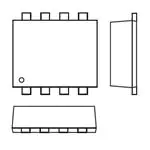
Package Dimensions
EMH2314-TL-H
°C/W
125
• Package
: EMH8
• JEITA, JEDEC
:• Minimum Packing Quantity : 3,000 pcs./reel
0.2
0.125
5
Taping Type : TL
Marking
MP
2.1
1.7
8
Unit
Product & Package Information
unit : mm (typ)
7045-002
0.2
Value
TL
1
LOT No.
0.2
4
0.5
0.05
0.75
2.0
1 : Source1
2 : Gate1
3 : Source2
4 : Gate2
5 : Drain2
6 : Drain2
7 : Drain1
8 : Drain1
Electrical Connection
8
7
6
5
1
2
3
4
EMH8
ORDERING INFORMATION
See detailed ordering and shipping information on page 2 of this data sheet.
Semiconductor Components Industries, LLC, 2014
July, 2014
72214HK TC-00003140/51612TKIM PE No.8759-1/5
�EMH2314
Electrical Characteristics at Ta=25°C
Parameter
Symbol
Drain-to-Source Breakdown Voltage
Zero-Gate Voltage Drain Current
Gate-to-Source Leakage Current
Forward Transconductance
Static Drain-to-Source On-State Resistance
Ratings
min
typ
max
Unit
V(BR)DSS
IDSS
ID= --1mA, VGS=0V
VGS(th)
gFS
VDS= --6V, ID= --1mA
VDS= --6V, ID= --2.5A
11
RDS(on)1
ID= --2.5A, VGS= --4.5V
28
37
mW
RDS(on)2
ID= --1.5A, VGS= --2.5V
53
75
mW
RDS(on)3
ID= --0.5A, VGS= --1.8V
133
200
mW
IGSS
Gate Threshold Voltage
Conditions
Input Capacitance
Ciss
Output Capacitance
Coss
--12
V
VDS= --12V, VGS=0V
VGS=±8V, VDS=0V
--0.4
VDS= --6V, f=1MHz
--10
mA
±10
mA
--1.3
V
S
1300
pF
158
pF
Reverse Transfer Capacitance
Crss
143
pF
Turn-ON Delay Time
td(on)
16
ns
Rise Time
tr
77
ns
Turn-OFF Delay Time
td(off)
79
ns
Fall Time
tf
58
ns
Total Gate Charge
Qg
12
nC
Gate-to-Source Charge
Qgs
3
nC
Gate-to-Drain “Miller” Charge
Qgd
Forward Diode Voltage
VSD
See specified Test Circuit.
VDS= --6V, VGS= --4.5V, ID= --5A
2
IS= --5A, VGS=0V
--0.9
nC
--1.2
V
Product parametric performance is indicated in the Electrical Characteristics for the listed test conditions, unless otherwise noted. Product performance may not be
indicated by the Electrical Characteristics if operated under different conditions.
Switching Time Test Circuit
0V
--4.5V
VDD= --6V
VIN
ID= --2.5A
RL=2.4Ω
VIN
D
PW=10μs
D.C.≤1%
VOUT
G
P.G
50Ω
EMH2314
S
Ordering Information
Device
EMH2314-TL-H
Package
Shipping
memo
EMH8
3,000pcs./reel
Pb-Free and Halogen Free
No.8759-2/5
�EMH2314
--3.0
--2.5
--2.0
--1.5
--1.6V
--0.1
--0.2
--0.3
--0.4
--0.5
--0.6
--0.7
--0.8
--0.9
Drain-to-Source Voltage, VDS -- V
ID= --0.5A
--1.5A
--2.5A
100
80
60
40
20
0
--1
--2
--3
--4
--5
--6
--7
10
7
5
3
2
=
Ta
5°C
--2
1.0
7
5
25
75
°C
°C
2
3
5 7 --0.1
2
3
5 7 --1.0
2
3
--0.5
, I D=
--1.8V
=
V GS
140
120
100
80
= --1.5A
2.5V, I D
-=
V GS
I = --2.5A
VGS= --4.5V, D
60
40
20
--20
0
20
40
60
80
100
120
140
160
IT16896
IS -- VSD
VGS=0V
3
2
--1.0
7
5
3
2
--0.1
7
5
SW Time -- ID
--0.4
--0.6
--0.8
--1.0
Forward Diode Voltage, VSD -- V
Ciss, Coss, Crss -- VDS
--1.2
--1.4
HD16898
f=1MHz
5
Ciss, Coss, Crss -- pF
2
td(off)
100
tf
7
5
tr
3
td(on)
2
3
--0.2
7
3
2
0
10000
VDD= --6V
VGS= --4.5V
10
--0.1
--0.01
5 7 --10
HD16897
Drain Current, ID -- A
5
--3.0
IT16894
3
2
0.1
--0.01
7
--2.5
A
160
--10
7
5
3
2
1000
--2.0
Ambient Temperature, Ta -- °C
VDS= --6V
3
2
--1.5
180
IT16895
gFS -- ID
--1.0
RDS(on) -- Ta
0
--60 --40
--8
Source Current, IS -- A
Forward Transconductance, gFS -- s
Gate-to-Source Voltage, VGS -- V
100
7
5
--0.5
Gate-to-Source Voltage, VGS -- V
Static Drain-to-Source
On-State Resistance, RDS(on) -- mΩ
Static Drain-to-Source
On-State Resistance, RDS(on) -- mΩ
160
120
0
200
180
0
0
--1.0
Ta=25°C
140
--2
IT16893
RDS(on) -- VGS
200
--3
--1
VGS= --1.3V
0
--4
--25°C
0
--5
25°C
--0.5
Switching Time, SW Time -- ns
--6
--3.5
--1.0
VDS= --6V
Ta=75
°C
--2.
5V
--3.0
V
8V
.
--1
Drain Current, ID -- A
Drain Current, ID -- A
--4.0
--4.5V
--8.0V
--4.5
ID -- VGS
--7
Ta=--2
5°C
75°C
25°C
ID -- VDS
--5.0
5
7
--1.0
3
2
Ciss
1000
7
5
3
Coss
2
2
Drain Current, ID -- A
3
5
7
100
--10
IT16899
Crss
0
--1
--2
--3
--4
--5
--6
--7
--8
--9
--10 --11 --12
Drain-to-Source Voltage, VDS -- V
IT16900
No.8759-3/5
�EMH2314
VGS -- Qg
--100
7
5
3
2
VDS= --6V
ID= --5A
--4.0
--3.5
Drain Current, ID -- A
Gate-to-Source Voltage, VGS -- V
--4.5
--3.0
--2.5
--2.0
--1.5
--1.0
--0.5
0
0
1
2
3
4
5
6
7
8
9
10
11
Total Gate Charge, Qg -- nC
ID= --5A
0m
ms
s
n(
Ta
=
tio
25
°C
)
Operation in this area
is limited by RDS(on).
Ta=25°C
Single pulse
When mounted on ceramic substrate
(900mm2×0.8mm)
--0.01
--0.01 2 3
12
op
10
10
era
--1.0
7
5
3
2
--0.1
7
5
3
2
DC
1
1m00μs
s
5 7--0.1
2 3
5 7--1.0 2 3
5 7--10
Drain-to-Source Voltage, VDS -- V
2 3
5 7--100
HD16902
5
5
When mounted on ceramic substrate
(900mm2×0.8mm)
1.2
Power Dissipation, PD -- W
IDP= --20A(PW≤10μs)
IT16901
PD -- Ta
1.4
--10
7
5
3
2
SOA
1.0
To
t
al
0.8
1u
0.6
di
ss
ip
at
ni
t
io
n
0.4
0.2
0
0
25
50
75
100
125
150
Ambient Temperature, Ta -- °C
RθJA -- Pulse Time
Thermal Resistance, RθJA -- ºC/W
1000
100
10
175
HD16903
Duty Cycle=0.5
0.2
0.1
0.05
0.02
0.01
1.0
lse
le Pu
Sing
0.1
0.000001 2
3
5 70.00001 2
3
5 70.0001
2
3
5 7 0.001
2
3
5 7 0.01
Pulse Time, PT -- s
2
3
7 0.1
2
3
5
7 1.0
2
3
7 10
HD
No.8759-4/5
�EMH2314
Outline Drawing
EMH2314-TL-H
Land Pattern Example
Mass (g) Unit
0.008 mm
* For reference
Unit: mm
1.9
0.4
0.3
0.5
Note on usage : Since the EMH2314 is a MOSFET product, please avoid using this device in the vicinity of
highly charged objects.
ON Semiconductor and the ON logo are registered trademarks of Semiconductor Components Industries, LLC (SCILLC) or its subsidiaries in the United States
and/or other countries. SCILLC owns the rights to a number of patents, trademarks, copyrights, trade secrets, and other intellectual property. A listing of
SCILLC’s product/patent coverage may be accessed at www.onsemi.com/site/pdf/Patent-Marking.pdf . SCILLC reserves the right to make changes without
further notice to any products herein. SCILLC makes no warranty, representation or guarantee regarding the suitability of its products for any particular purpose,
nor does SCILLC assume any liability arising out of the application or use of any product or circuit, and specifically disclaims any and all liability, including without
limitation special, consequential or incidental damages. “Typical” parameters which may be provided in SCILLC data sheets and/or specifications can and do
vary in different applications and actual performance may vary over time. All operating parameters, including “Typicals” must be validated for each customer
application by customer’s technical experts. SCILLC does not convey any license under its patent rights nor the rights of others. SCILLC products are not
designed, intended, or authorized for use as components in systems intended for surgical implant into the body, or other applications intended to support or
sustain life, or for any other application in which the failure of the SCILLC product could create a situation where personal injury or death may occur. Should
Buyer purchase or use SCILLC products for any such unintended or unauthorized application, Buyer shall indemnify and hold SCILLC and its officers,
employees, subsidiaries, affiliates, and distributors harmless against all claims, costs, damages, and expenses, and reasonable attorney fees arising out of,
directly or indirectly, any claim of personal injury or death associated with such unintended or unauthorized use, even if such claim alleges that SCILLC was
negligent regarding the design or manufacture of the part. SCILLC is an Equal Opportunity/Affirmative Action Employer. This literature is subject to all applicable
copyright laws and is not for resale in any manner.
PS No.8759-5/5
�