Is Now Part of
To learn more about ON Semiconductor, please visit our website at
www.onsemi.com
Please note: As part of the Fairchild Semiconductor integration, some of the Fairchild orderable part numbers
will need to change in order to meet ON Semiconductor’s system requirements. Since the ON Semiconductor
product management systems do not have the ability to manage part nomenclature that utilizes an underscore
(_), the underscore (_) in the Fairchild part numbers will be changed to a dash (-). This document may contain
device numbers with an underscore (_). Please check the ON Semiconductor website to verify the updated
device numbers. The most current and up-to-date ordering information can be found at www.onsemi.com. Please
email any questions regarding the system integration to Fairchild_questions@onsemi.com.
ON Semiconductor and the ON Semiconductor logo are trademarks of Semiconductor Components Industries, LLC dba ON Semiconductor or its subsidiaries in the United States and/or other countries. ON Semiconductor owns the rights to a number
of patents, trademarks, copyrights, trade secrets, and other intellectual property. A listing of ON Semiconductor’s product/patent coverage may be accessed at www.onsemi.com/site/pdf/Patent-Marking.pdf. ON Semiconductor reserves the right
to make changes without further notice to any products herein. ON Semiconductor makes no warranty, representation or guarantee regarding the suitability of its products for any particular purpose, nor does ON Semiconductor assume any liability
arising out of the application or use of any product or circuit, and specifically disclaims any and all liability, including without limitation special, consequential or incidental damages. Buyer is responsible for its products and applications using ON
Semiconductor products, including compliance with all laws, regulations and safety requirements or standards, regardless of any support or applications information provided by ON Semiconductor. “Typical” parameters which may be provided in ON
Semiconductor data sheets and/or specifications can and do vary in different applications and actual performance may vary over time. All operating parameters, including “Typicals” must be validated for each customer application by customer’s
technical experts. ON Semiconductor does not convey any license under its patent rights nor the rights of others. ON Semiconductor products are not designed, intended, or authorized for use as a critical component in life support systems or any FDA
Class 3 medical devices or medical devices with a same or similar classification in a foreign jurisdiction or any devices intended for implantation in the human body. Should Buyer purchase or use ON Semiconductor products for any such unintended
or unauthorized application, Buyer shall indemnify and hold ON Semiconductor and its officers, employees, subsidiaries, affiliates, and distributors harmless against all claims, costs, damages, and expenses, and reasonable attorney fees arising out
of, directly or indirectly, any claim of personal injury or death associated with such unintended or unauthorized use, even if such claim alleges that ON Semiconductor was negligent regarding the design or manufacture of the part. ON Semiconductor
is an Equal Opportunity/Affirmative Action Employer. This literature is subject to all applicable copyright laws and is not for resale in any manner.
�FAN156
Low Voltage Comparator
Features
Description
The FAN156 is a low-power single comparator that
typically consumes less than 10 µA of supply current. It
is guaranteed to operate at a low voltage of 1.6 V and is
fully operational up to 5.5 V, making it convenient for
use in 1.8, 3.0 V, and 5.0 V systems.
Low Supply Current: IDD 6 μA (Typical)
Single Power Supply Operation
Wide Common-Mode Input Voltage Range
Push-Pull Output Circuit
The FAN156 has a complementary push-pull P- and Nchannel output stage capable of driving a rail-to-rail
output swing with a load ranging up to 5.0 mA.
Low Input Bias Current
Internal Hysteresis
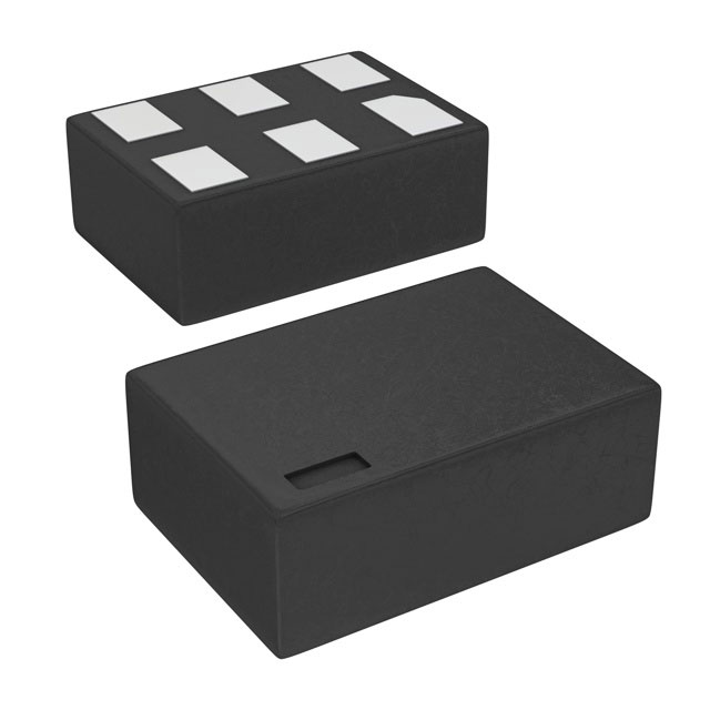
Packaged in MicroPak™ 6
Applications
Mobile Phones
Alarm and Security Systems
Personal Digital Assistants
Figure 1. Functional Diagram
Ordering Information
Part Number
FAN156L6X
Top
Mark
Operating
Temperature Range
CN
-40 to 85°C
© 2010 Fairchild Semiconductor Corporation
FAN156 • Rev. 1.0.1
Package
6-Lead, MicroPak™, 1 x 1.45 mm Wide
Packing
Method
5000 Units on
Tape and Reel
www.fairchildsemi.com
FAN156 — Low Voltage Comparator
December 2012
�FAN156 — Low Voltage Comparator
Pin Configuration
OUT 1
6
V DD
VSS 2
5
NC
IN+
4
IN-
3
Figure 2. Pin Configuration (Top-Through View)
Pin Definitions
Pin #
Name
Description
1
OUT
Comparator Output
2
VSS
Negative Supply Voltage
3
IN+
Non-Inverting Input
4
IN-
Inverting Input
5
NC
No Connect
6
VDD
Positive Supply Voltage
Function Table
Inputs
Outputs
IN(-) > IN(+)
Output LOW
IN(+) > IN(-)
Output HIGH
VDD
VOUT
VIN(-)
VDD
VOUT
VOUT
VOUT
VIN (+)
VIN (-)
VIN(+)
Figure 3. VIN vs. VOUT
© 2010 Fairchild Semiconductor Corporation
FAN156 • Rev. 1.0.1
www.fairchildsemi.com
2
�Stresses exceeding the absolute maximum ratings may damage the device. The device may not function or be
operable above the recommended operating conditions and stressing the parts to these levels is not recommended.
In addition, extended exposure to stresses above the recommended operating conditions may affect device reliability.
The absolute maximum ratings are stress ratings only.
Symbol
Parameter
Condition
VDD to VSS Supply Voltage
DVIN
VIN
Min.
Max.
-3.0
+3.0
0
6.0
Differential Input Voltage
Unit
V
±6
Input Voltage
VSS to VDD
V
ts
Output Short Circuit Duration(1)
Indefinite
s
TJ
Junction Temperature
+150
°C
TSTG
+150
°C
PD
Storage Temperature Range
Power Dissipation
194
mW
ΘJA
Thermal Resistance
335
°C/W
IEC 61000-4-2 System ESD
ESD
JEDEC JESD22-A114, Human Body
Model
JEDEC JESD22-C101, Charged
Device Model
-65
Air Gap
15
Contact
8
All Pins
8
Pin to Pin: IN(-), IN(+)
to VDD or VSS
12
All Pins
2
FAN156 — Low Voltage Comparator
Absolute Maximum Ratings
kV
Note:
1. The maximum total power dissipation must not be exceeded.
Recommended Operating Conditions
The Recommended Operating Conditions table defines the conditions for actual device operation. Recommended
operating conditions are specified to ensure optimal performance to the datasheet specifications. Fairchild does not
recommend exceeding them or designing to Absolute Maximum Ratings.
Symbol
Parameter
Condition
VDD to VSS Power Supply
VDD
Power Supply
VIN
Input Voltage
IOH/IOL
TA
Output Sink/Source Current
VSS 0 V
Max.
-2.75
+2.75
0
5.50
1.6
5.5
V
VSS to VDD
V
VDD 5.0 V
5
VDD 3.0 V
3
VDD 1.6 V
1
Operating Temperature, Free Air
© 2010 Fairchild Semiconductor Corporation
FAN156 • Rev. 1.0.1
Min.
-40
+85
Unit
V
mA
°C
www.fairchildsemi.com
3
�Symbol
Parameter
Condition
Min.
Typ.
-15
±1
Max.
Unit
+15
mV
VDD=5.5V, VSS=GND, and TA=+25°C
VHYS
Input Hysteresis
VCM=0.5 VDD
VIO
Input Offset Voltage(2)
VCM=0.5 VDD
IIO
Input Offset Current
10
pA
II
Input Bias Current
10
pA
VCM
CMRR
IDD
PSRR
Common Mode Input Voltage
4
VSS
Common Mode Rejection Ratio(3)
VDD
VCM=VDD
68
Supply Current
6
Power Supply Rejection Ratio
(3)
∆VDD=0.5 V
mV
45
17
80
VO=VDD
60
VO=VSS
90
ISINK=5.0 mA
0.1
V
dB
µA
dB
IOS
Output Short Circuit Current
VOL
Low-Level Output Voltage
VOH
High-Level Output Voltage
ISOURCE=5.0 mA
5.4
V
tPLH
Propagation Delay (Turn-On)
Overdrive 20 mV,
CL=15 pF
0.40
µs
tPHL
Propagation Delay (Turn-Off)
Overdrive=20 mV,
CL=15 pF
0.42
µs
tTLH
tTHL
(4)
Response Time, Output Rise/Fall
5.2
mA
0.3
4.0
CL=50 pF
FAN156 — Low Voltage Comparator
Electrical Characteristics
V
ns
5.4
VDD=3V, VSS=GND, and TA=+25°C
VHYS
Input Hysteresis
VCM=0.5 VDD
(2)
Input Offset Voltage
IIO
Input Offset Current
10
pA
II
Input Bias Current
10
pA
CMRR
IDD
PSRR
Common Mode Input Voltage
Common Mode Rejection Ratio
VCM=VDD
5.5
Power Supply Rejection Ratio(3)
∆VDD=0.5 V
27
35
ISINK=3.0 mA
VOH
High-Level Output Voltage
ISOURCE=3.0 mA
tPLH
Propagation Delay (Turn-On)
tPHL
Propagation Delay (Turn-Off)
(4)
0.15
V
15.0
µA
dB
dB
mA
0.35
V
2.85
V
Overdrive=20 mV,
CL=15 pF
0.45
µs
Overdrive=20 mV,
CL=15 pF
0.47
µs
CL=50pF
2.65
mV
VDD
80
VO=VSS
Low-Level Output Voltage
Response Time, Output Rise/Fall
45
VO=VDD
VOL
+15
60
Supply Current
Output Short Circuit Current
tTHL
±1
VSS
(3)
IOS
tTLH
-15
mV
VIO
VCM
VCM=0.5 VDD
4
6.1
6.2
ns
Continued on the following page…
© 2010 Fairchild Semiconductor Corporation
FAN156 • Rev. 1.0.1
www.fairchildsemi.com
4
�Symbol
Parameter
Condition
Min.
Typ.
Max.
Unit
+15
mV
VDD 1.6V, VSS GND, and TA=+25°C
VHYS
Input Hysteresis
VCM=0.5 VDD
VIO
Input Offset Voltage(2)
VCM=0.5 VDD
IIO
Input Offset Current
10
pA
II
Input Bias Current
10
pA
VCM
CMRR
IDD
PSRR
Common Mode Input Voltage
VCM=VDD
∆VDD=0.5 V
VO=VSS
7.5
0.10
Low-Level Output Voltage
ISINK=1.0 mA
VOH
High-Level Output Voltage
ISOURCE=1.0 mA
tPLH
Propagation Delay (Turn-On)
tPHL
Propagation Delay (Turn-Off)
(4)
15
µA
dB
mA
0.25
V
1.50
V
Overdrive=20 Mv,
CL=15pF
0.52
µs
Overdrive=20 Mv,
CL=15 pF
0.54
µs
CL=50 pF
1.35
V
dB
80
5.5
VOL
Response Time, Output Rise/Fall
45
VO=VDD
Output Short Circuit Current
tTHL
VDD
5
(3)
mV
56
Supply Current
Power Supply Rejection Ratio
±1
VSS
Common Mode Rejection Ratio(3)
IOS
tTLH
3.5
-15
16.5
13.0
FAN156 — Low Voltage Comparator
Electrical Characteristics (Continued)
ns
Notes:
2. Differential input switching level is guaranteed at the minimum or maximum offset voltage, minus or plus half the
maximum hysteresis voltage.
3. Guaranteed by design and characterization data.
4. Input signal: 1 kHz, square-wave signal with 10 ns edge rate.
© 2010 Fairchild Semiconductor Corporation
FAN156 • Rev. 1.0.1
www.fairchildsemi.com
5
�900
7.50
800
7.00
700
1.6 VDD
600
3.0 VDD
500
5.5 VDD
6.50
ICC (µA)
I DD , Sopply Current (µA)
8.00
6.00
5.50
300
VDD=1.6V
5.00
200
VDD=3.0V
4.50
400
100
VDD=5.5V
0
4.00
-55 ⁰C
-40 ⁰C
-25 ⁰C
25 ⁰C
85 ⁰C
0.01
95 ⁰C
0.1
1
10
100
1000
Temp. =25C
Frequency (Khz)
CL = 15pF
TA, Ambient Temperature
Figure 4. Supply Current vs. Temperature
Figure 5.
Supply Current vs. Output Transition
Frequency
FAN156 — Low Voltage Comparator
Typical Performance Characteristics
6
5.5
VOH, Output Voltage HIGH State (V)
I DD , Supply Current (µA)
12
10
8
6
-40 ⁰C
4
25 ⁰C
2
85 ⁰C
0
5
4.5
4
3.5
3
2.5
2
VDD=1.6V
1.5
0
0.5
1
1.5
2
2.5
3
3.5
4
4.5
5
5.5
6
VDD=3.0V
1
VDD, Supply Voltage (V)
VDD=5.5V
0.5
0
2
4
6
8
10
ISOURCE, Output Source Current (mA)
Figure 6.
Supply Current vs. Supply Voltage
Figure 7. Output HIGH vs. Output Drive Current
380
360
340
100
320
tPHL (ns)
VOL , Output Voltage Low (mV)
400
1000
VDD=1.6V
10
300
280
VDD=3.0V
1.6VDD
260
VDD=5.5V
3.0VDD
240
5.5VDD
1
220
0.10
1.00
10.00
200
ISINK , Output Sink Current (mA)
-60
-40
-20
0
20
40
60
80
100
Temperature
Figure 8.
Figure 9. Propagation Delay (tPHL) vs. Temperature
Output LOW vs. Output Drive Current
© 2010 Fairchild Semiconductor Corporation
FAN156 • Rev. 1.0.1
www.fairchildsemi.com
6
�300
500
280
260
450
Delay (nS)
240
tPLH (ns)
400
350
300
220
200
180
1.6VDD
3.0VDD
160
tpLH
140
tpHL
120
250
5.5VDD
100
200
-60
-40
-20
0
20
40
60
80
0
100
Figure 10. Propagation Delay (tPLH) vs. Temperature
100
150
200
250
Overdrive (mV)
Figure 11. Propagation Delay vs. Input Overdrive
3
2
TA = 25°C
7
6
1
5
Voltage (V)
Input Common-Mode Voltage Range (V)
50
VDD=3.0V
Temp. =25°C
Temperature
FAN156 — Low Voltage Comparator
Typical Performance Characteristics (Continued)
0
-1
-2
4
3
2
VDD
1
Output
0
-3
0
1
2
3
4
5
6
50
100
Input Overdrive = 50mV
150
200
250
300
Time (µS)
VS, Supply Voltage (V)
Figure 12. Input Common-Mode Voltage Range vs.
Supply Voltage
© 2010 Fairchild Semiconductor Corporation
FAN156 • Rev. 1.0.1
Figure 13.Power-Up Delay
www.fairchildsemi.com
7
�FAN156 — Low Voltage Comparator
Physical Dimensions
2X
0.05 C
1.45
B
2X
(1)
0.05 C
(0.254)
(0.49)
5X
1.00
(0.75)
PIN 1 IDENTIFIER
5
(0.52)
1X
A
TOP VIEW
0.55MAX
(0.30)
6X
PIN 1
0.05 C
0.05
0.00
RECOMMENED
LAND PATTERN
0.05 C
C
0.25
0.15 6X
1.0
DETAIL A
0.10
0.05
0.45
0.35
0.10
0.00 6X
C B A
C
0.40
0.30
0.35 5X
0.25
0.40 5X
0.30
0.5
(0.05)
6X
Notes:
BOTTOM VIEW
(0.13)
4X
DETAIL A
PIN 1 TERMINAL
0.075 X 45
CHAMFER
1. CONFORMS TO JEDEC STANDARD M0-252 VARIATION UAAD
2. DIMENSIONS ARE IN MILLIMETERS
3. DRAWING CONFORMS TO ASME Y14.5M-1994
4. FILENAME AND REVISION: MAC06AREV4
5. PIN ONE IDENTIFIER IS 2X LENGTH OF ANY
OTHER LINE IN THE MARK CODE LAYOUT.
Figure 14.
6-Lead, MicroPak™, 1 x 1.45 mm Wide
Package drawings are provided as a service to customers considering Fairchild components. Drawings may change in any manner
without notice. Please note the revision and/or date on the drawing and contact a Fairchild Semiconductor representative to verify or
obtain the most recent revision. Package specifications do not expand the terms of Fairchild’s worldwide terms and conditions, specifically the
warranty therein, which covers Fairchild products.
Always visit Fairchild Semiconductor’s online packaging area for the most recent package drawings:
http://www.fairchildsemi.com/packaging/.
Tape and Reel Specifications
Please visit Fairchild Semiconductor’s online packaging area for the most recent tape and reel specifications:
http://www.fairchildsemi.com/products/logic/pdf/micropak_tr.pdf.
Package Designator
L6X
© 2010 Fairchild Semiconductor Corporation
FAN156 • Rev. 1.0.1
Tape Section
Cavity Number
Leader (Start End)
125 (Typical)
Cavity Status Cover Type Status
Empty
Sealed
Carrier
5000
Filled
Sealed
Trailer (Hub End)
75 (Typical)
Empty
Sealed
www.fairchildsemi.com
8
�FAN156 — Low Voltage Comparator
© 2010 Fairchild Semiconductor Corporation
FAN156 • Rev. 1.0.1
www.fairchildsemi.com
9
�ON Semiconductor and
are trademarks of Semiconductor Components Industries, LLC dba ON Semiconductor or its subsidiaries in the United States and/or other countries.
ON Semiconductor owns the rights to a number of patents, trademarks, copyrights, trade secrets, and other intellectual property. A listing of ON Semiconductor’s product/patent
coverage may be accessed at www.onsemi.com/site/pdf/Patent−Marking.pdf. ON Semiconductor reserves the right to make changes without further notice to any products herein.
ON Semiconductor makes no warranty, representation or guarantee regarding the suitability of its products for any particular purpose, nor does ON Semiconductor assume any liability
arising out of the application or use of any product or circuit, and specifically disclaims any and all liability, including without limitation special, consequential or incidental damages.
Buyer is responsible for its products and applications using ON Semiconductor products, including compliance with all laws, regulations and safety requirements or standards,
regardless of any support or applications information provided by ON Semiconductor. “Typical” parameters which may be provided in ON Semiconductor data sheets and/or
specifications can and do vary in different applications and actual performance may vary over time. All operating parameters, including “Typicals” must be validated for each customer
application by customer’s technical experts. ON Semiconductor does not convey any license under its patent rights nor the rights of others. ON Semiconductor products are not
designed, intended, or authorized for use as a critical component in life support systems or any FDA Class 3 medical devices or medical devices with a same or similar classification
in a foreign jurisdiction or any devices intended for implantation in the human body. Should Buyer purchase or use ON Semiconductor products for any such unintended or unauthorized
application, Buyer shall indemnify and hold ON Semiconductor and its officers, employees, subsidiaries, affiliates, and distributors harmless against all claims, costs, damages, and
expenses, and reasonable attorney fees arising out of, directly or indirectly, any claim of personal injury or death associated with such unintended or unauthorized use, even if such
claim alleges that ON Semiconductor was negligent regarding the design or manufacture of the part. ON Semiconductor is an Equal Opportunity/Affirmative Action Employer. This
literature is subject to all applicable copyright laws and is not for resale in any manner.
PUBLICATION ORDERING INFORMATION
LITERATURE FULFILLMENT:
Literature Distribution Center for ON Semiconductor
19521 E. 32nd Pkwy, Aurora, Colorado 80011 USA
Phone: 303−675−2175 or 800−344−3860 Toll Free USA/Canada
Fax: 303−675−2176 or 800−344−3867 Toll Free USA/Canada
Email: orderlit@onsemi.com
© Semiconductor Components Industries, LLC
N. American Technical Support: 800−282−9855 Toll Free
USA/Canada
Europe, Middle East and Africa Technical Support:
Phone: 421 33 790 2910
Japan Customer Focus Center
Phone: 81−3−5817−1050
www.onsemi.com
1
ON Semiconductor Website: www.onsemi.com
Order Literature: http://www.onsemi.com/orderlit
For additional information, please contact your local
Sales Representative
www.onsemi.com
�