FAN2103 — TinyBuck™
3 A, 24 V Input, Integrated Synchronous Buck
Regulator
Features
Description
The FAN2103 TinyBuck™ is an easy-to-use, cost- and
space-efficient, 3 A synchronous buck solution. It
enables designers to solve high current requirements in
a small area with minimal external components.
3 A Output Current
Over 95% Efficiency
Fully Synchronous Operation with Integrated
Schottky Diode on Low-side MOSFET Boosts
Efficiency
Programmable Frequency Operation (200 KHz to
600 KHz)
Power-good Signal
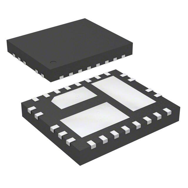
5x6 mm, 25-pin, 3-Pad MLP
Accepts Ceramic Capacitors on Output
External Compensation for Flexible Design
Wide Input Range: 3 V to 24 V
Output Voltage Range: 0.8 V to 90%VIN
The summing current mode modulator uses lossless
current sensing for current feedback and over-current,
and includes voltage feedforward.
Fairchild’s advanced BiCMOS power process, combined
with low RDS(ON) internal MOSFETs and a thermally
efficient MLP package provide the ability to dissipate
high power in a small package.
Programmable Over-Current Limit
Output over-voltage, under-voltage, and thermal
shutdown protections plus power-good, help protect the
devices from damage during fault conditions.
Under-Voltage, Over-Voltage, and
Thermal Protections
Related Application Notes
Input Under-Voltage Lockout
Applications
External compensation, programmable switching
frequency, and current limit features allow for design
optimization and flexibility.
Graphics Cards
TinyCalc™ Design Tool
AN-6033 — TinyCalc™ Design Tool Guide
AN-5067 – PCB Land Pattern Design and Surface
Mount Guidelines for MLP Packages
Battery-powered Equipment
Set-top Boxes
Point-of-load Regulation
Servers
Ordering Information
Part Number
Operating
Temperature Range
FAN2103MPX
-10°C to 85°C
FAN2103EMPX
-40°C to 85°C
© 2007 Fairchild Semiconductor Corporation
FAN2103 • Rev. 1.0.9
Package
Packing Method
25-Pin Molded Leadless Package (MLP) 5 x 6 mm
Tape and Reel
www.fairchildsemi.com
FAN2103 — TinyBuck™ 3 A, 24 V Input, Integrated Synchronous Buck Regulator
August 2014
�FAN2103 — TinyBuck™ 3 A, 24 V Input, Integrated Synchronous Buck Regulator
Typical Application Diagram
Figure 1. Typical Application
Block Diagram
BOOT
VCC
Boot
Diode
Current Limit
Comparator
IILIM
VIN
ILIM
Def Level
COMP
CBOOT
Error
Amplifier
R
PWM
Comparator
FB
Q
VOUT
SW
S
SS
Gate
Drive
Circuit
VREF
L
COUT
EN
OSC
RAMP
GEN
Summing
Amplifier
Current
Sense
GND
RAMP
Figure 2. Block Diagram
© 2007 Fairchild Semiconductor Corporation
FAN2103 • Rev. 1.0.9
www.fairchildsemi.com
2
�VIN
VIN
SW
SW
SW
4
5
6
7
8
15
14
EN
16
AGND
VCC
17
ILIM
9
VIN
3
18
R(T)
10
VIN
2
19
FB
11
BOOT
1
20
COMP
22
PGND
P3
GND
SW
SW
12
24
PGND
21
PGND
P1
SW
SW
SW
PGOOD 13
25
NC
P2
VIN
23
RAMP
Figure 3. MLP 5 x 6 mm Pin Configuration (Bottom View)
Pin Definitions
Pin
Name
Description
P1, 6-12
SW
Switching Node.
P2, 2-5
VIN
Power Input Voltage. Connect to the main input power source.
P3, 21-23
PGND
Power Ground. Power return and Q2 source.
1
BOOT
High-side Drive BOOT Voltage. Connect through capacitor (CBOOT) to SW. The IC includes
an internal synchronous bootstrap diode to recharge the capacitor on this pin to VCC when
SW is LOW.
13
PGOOD
Power-Good Flag. An open-drain output that pulls LOW when FB is outside a ±10% range
of the reference when EN is HIGH. PGOOD does not assert HIGH until the fault latch is
enabled.
14
EN
ENABLE. Enables operation when pulled to logic HIGH or left open. Toggling EN resets the
regulator after a latched fault condition. This input has an internal pull-up when the IC is
functioning normally. When a latched fault occurs, EN is discharged by a current sink.
15
VCC
16
AGND
17
ILIM
Current Limit. A resistor (RILIM) from this pin to AGND can be used to program the currentlimit trip threshold lower than the default setting.
18
R(T)
Oscillator Frequency. A resistor (RT) from this pin to AGND sets the PWM switching
frequency.
19
FB
Output Voltage Feedback. Connect through a resistor divider to the output voltage.
20
COMP
24
NC
25
RAMP
FAN2103 — TinyBuck™ 3 A, 24 V Input, Integrated Synchronous Buck Regulator
Pin Configuration
Input Bias Supply for IC. The IC’s logic and analog circuitry are powered from this pin.
Analog Ground. The signal ground for the IC. All internal control voltages are referred to
this pin. Tie this pin to the ground island/plane through the lowest impedance connection.
Compensation. Error amplifier output. Connect the external compensation network between
this pin and FB.
No Connect. This pin is not used.
Ramp Amplitude. A resistor (RRAMP) connected from this pin to VIN sets the ramp amplitude
and provides voltage feedforward functionality.
© 2007 Fairchild Semiconductor Corporation
FAN2103 • Rev. 1.0.9
www.fairchildsemi.com
3
�Stresses exceeding the absolute maximum ratings may damage the device. The device may not function or be
operable above the recommended operating conditions and stressing the parts to these levels is not recommended.
In addition, extended exposure to stresses above the recommended operating conditions may affect device reliability.
The absolute maximum ratings are stress ratings only.
Parameter
Conditions
Min.
VIN to PGND
VCC to AGND
AGND = PGND
BOOT to PGND
BOOT to SW
SW to PGND
ESD
Unit
28
V
6
V
35
V
-0.3
6.0
V
-5
30
V
-0.3
VCC+0.3
V
Transient (t < 20 ns, f < 600 KHz)
All other pins
Max.
Human Body Model, JEDEC JESD22-A114
2.0
Charged Device Model, JEDEC JESD22-C101
2.5
kV
Recommended Operating Conditions
The Recommended Operating Conditions table defines the conditions for actual device operation. Recommended
operating conditions are specified to ensure optimal performance to the datasheet specifications. Fairchild does not
recommend exceeding them or designing to absolute maximum ratings.
Symbol
Parameter
Conditions
VCC
Bias Voltage
VCC to AGND
VIN
Supply Voltage
VIN to PGND
TA
Ambient Temperature
TJ
Junction Temperature
Min.
Typ.
Max.
Unit
4.5
5.0
5.5
V
3
24
V
FAN2103M
-10
+85
°C
FAN2103EM
-40
+85
°C
+125
°C
Max.
Unit
+150
°C
Thermal Information
Symbol
TSTG
Parameter
Min.
Storage Temperature
Typ.
-65
TL
Lead Soldering Temperature, 10 Seconds
+300
°C
TVP
Vapor Phase, 60 Seconds
+215
°C
Infrared, 15 Seconds
+220
°C
TI
JC
J-PCB
PD
Thermal Resistance: Junction-to-Case
P1 (Q2)
4
°C/W
P2 (Q1)
7
°C/W
P3
4
°C/W
Thermal Resistance: Junction-to-Mounting Surface
(1)
35
°C/W
(1)
Power Dissipation, TA = 25°C
FAN2103 — TinyBuck™ 3 A, 24 V Input, Integrated Synchronous Buck Regulator
Absolute Maximum Ratings
2.8
W
Note:
1. Typical thermal resistance when mounted on a four-layer, two-ounce PCB, as shown in Figure 26. Actual results
are dependent on mounting method and surface related to the design.
© 2007 Fairchild Semiconductor Corporation
FAN2103 • Rev. 1.0.9
www.fairchildsemi.com
4
�Recommended operating conditions are the result of using the circuit shown in Figure 1 unless otherwise noted.
Parameter
Conditions
Min.
Typ.
Max.
Unit
8
12
mA
7
10
µA
4.3
4.5
V
Power Supplies
SW = Open, FB = 0.7 V, VCC = 5 V,
fSW = 600 KHz
VCC Current
Shutdown: EN = 0, VCC = 5 V
VCC UVLO Threshold
Rising VCC
4.1
Hysteresis
300
mV
Oscillator
Frequency
RT = 50 K
255
300
345
KHz
RT = 24 K
540
600
660
KHz
50
65
ns
(2)
Minimum On-Time
Ramp Amplitude, pk–pk
16 VIN, 1.8 VOUT, RT = 30 K,
RRAMP = 200 K
0.53
Minimum Off-Time(2)
V
100
150
ns
mV
Reference
Reference Voltage (VFB)
Temperature Coefficient
FAN2103M, 25°C
794
800
806
FAN2103EM, 25°C
795
800
805
mV
FAN2103M, -10 to +85°C
50
PPM
FAN2103EM, -40 to +85°C
70
PPM
Error Amplifier
DC Gain(2)
Gain Bandwidth Product(2)
VCC = 5 V
Output Voltage (VCOMP)
80
85
dB
12
15
MHz
0.4
3.2
V
Output Current, Sourcing
VCC = 5 V, VCOMP = 2.2 V
1.5
2.2
mA
Output Current, Sinking
VCC = 5 V, VCOMP = 1.2 V
0.8
1.2
mA
FB Bias Current
VFB = 0.8 V, 25°C
-850
-650
-450
Current Limit
RILIM Open
3.8
5.0
7.0
A
ILIM Current
25°C, VCC = 5 V
9
10
11
µA
nA
Protection and Shutdown
Over-Temperature Shutdown
Over-Temperature Hysteresis
+160
Internal IC Temperature
FAN2103 — TinyBuck™ 3 A, 24 V Input, Integrated Synchronous Buck Regulator
Electrical Specifications
°C
+30
°C
Over-Voltage Threshold
2 Consecutive Clock Cycles
110
115
120
%VOUT
Under-Voltage Shutdown
16 Consecutive Clock Cycles
68
73
78
%VOUT
Fault Discharge Threshold
Measured at FB Pin
250
mV
Fault Discharge Hysteresis
Measured at FB Pin (VFB ~500 mV)
250
mV
5.3
ms
6.7
ms
Soft-Start
VOUT to Regulation (T0.8)
Fault Enable/SSOK (T1.0)
Frequency = 600 KHz
Note:
2. Specifications guaranteed by design and characterization; not production tested.
© 2007 Fairchild Semiconductor Corporation
FAN2103 • Rev. 1.0.9
www.fairchildsemi.com
5
�Recommended operating conditions are the result of using the circuit shown in Figure 1 unless otherwise noted.
Parameter
Conditions
Min.
Typ.
Max.
Unit
EN Threshold, Rising
1.35
2.00
V
EN Hysteresis
250
mV
800
K
1
µA
Control Functions
EN Pull-up Resistance
EN Discharge Current
Auto-restart Mode
FB OK Drive Resistance
800
PGOOD Threshold
(Compared to VREF)
FB < VREF
-14
-11
-8
%VREF
FB > VREF
+7
+10
+13
%VREF
PGOOD Output Low
IOUT < 2 mA
0.4
V
© 2007 Fairchild Semiconductor Corporation
FAN2103 • Rev. 1.0.9
FAN2103 — TinyBuck™ 3 A, 24 V Input, Integrated Synchronous Buck Regulator
Electrical Specifications (Continued)
www.fairchildsemi.com
6
�1.20
1.005
1.10
I FB
V FB
1.010
1.000
0.995
1.00
0.90
0.990
0.80
-50
0
50
100
150
-50
0
o
150
Figure 5. Reference Bias Current (IFB) vs.
Temperature, Normalized
1500
1.02
1200
1.01
Frequency
Frequency (KHz)
100
Temperature ( C)
Figure 4. Reference Voltage (VFB) vs. Temperature,
Normalized
900
600
600KHz
1.00
300KHz
0.99
300
0.98
0
0
20
40
60
80
100
120
-50
140
0
50
100
150
o
RT (K)
Temperature ( C)
Figure 6. Frequency vs. RT
Figure 7.
Frequency vs. Temperature, Normalized
1.04
1.60
1.40
1.02
1.20
I ILIM
RDS
50
o
Temperature ( C)
FAN2103 — TinyBuck™ 3 A, 24 V Input, Integrated Synchronous Buck Regulator
Typical Characteristics
Q1 ~0.32 %/oC
1.00
Q2 ~0.35 %/oC
1.00
0.98
0.80
0.96
0.60
-50
0
50
100
150
-50
50
100
150
Temperature ( C)
Temperature ( C)
Figure 9.
Figure 8. RDS vs. Temperature, Normalized
(VCC = VGS = 5 V)
© 2007 Fairchild Semiconductor Corporation
FAN2103 • Rev. 1.0.9
0
o
o
ILIM Current (IILIM) vs. Temperature,
Normalized
www.fairchildsemi.com
7
�FAN2103
VCC
+5V
1.0µ
P2
15
VIN
8-20 VIN
10K
X5R
PGOOD
200K
3.3n
13
2 x 4.7µ
VOUT
X7R
NC 24
2.49K
62
COMP
2.49K
4.7n
RAMP
25
20
56p
FB
BOOT
1
19
* TDK
RLF7030T-3R3M4R1
4.7n
ILIM
0.1µ
17
VOUT
EN
200K
R(T)
P1
14
SW
3.3µ *
18
1.5W
30.1K
2.00K
4 x 22µ
AGND
4.7n
P3 PGND
16
X5R
390p
Figure 10. Application Circuit: 1.8 VOUT, 500 KHz
Typical Performance Characteristics
Typical operating characteristics using the circuit shown in Figure 10. VIN=16 V, VCC=5 V, unless otherwise specified.
Efficiency
100
Power Loss
1.0
0.9
90
0.8
85
0.7
80
0.6
Loss (W)
Efficiency (%)
95
75
70
0.3
Effi8V (%)
0.2
60
Effi18V (%)
0.1
1.00
1.50
2.00
2.50
Loss18V (W)
0.4
65
0.50
Loss8V (W)
0.5
Effi12V (%)
55
0.00
Loss12V (W)
0.0
0.00
3.00
0.50
1.00
2.00
2.50
3.00
Load Current (A)
Load Current (A)
Figure 11.
1.50
FAN2103 — TinyBuck™ 3 A, 24 V Input, Integrated Synchronous Buck Regulator
Application Circuit
1.8 VOUT Efficiency Over VIN vs. Load
Figure 12. 1.8 VOUT Dissipation Over VIN vs. Load
Regulation Characteristic
Efficiency
100
1.828
95
1.826
Efficiency (%)
Vo (V)
90
1.824
1.822
80
75
Vo8V (V)
1.820
85
Vo12V (V)
V IN =8V, 300KHz
70
Vo18V (V)
1.818
0.00
V IN =12V, 500Khz
65
0.50
1.00
1.50
2.00
Load Current (A)
2.50
0.00
3.00
1.00
1.50
2.00
2.50
3.00
Load Curr e nt (A)
Figure 13. 1.8 VOUT Regulation vs. Load
© 2007 Fairchild Semiconductor Corporation
FAN2103 • Rev. 1.0.9
0.50
Figure 14. 3.3 VOUT Efficiency vs. Load
(Circuit Values Changed)
www.fairchildsemi.com
8
�Typical operating characteristics using the circuit shown in Figure 10. VIN=12 V, VCC=5 V, unless otherwise specified.
Figure 15. SW and VOUT Ripple, 3 A Load
Figure 16. Startup with 1 V Pre-Bias on VOUT
Figure 17. Transient Response, 1.5-3 A Load
(Circuit Values Changed)
Figure 18. Re-start on Fault
Figure 19.
Startup, 3 A Load
© 2007 Fairchild Semiconductor Corporation
FAN2103 • Rev. 1.0.9
Figure 20.
FAN2103 — TinyBuck™ 3 A, 24 V Input, Integrated Synchronous Buck Regulator
Typical Performance Characteristics (Continued)
Shutdown, 3 A Load
www.fairchildsemi.com
9
�Initialization
Bias Supply
Once VCC exceeds the UVLO threshold and EN is HIGH,
the IC checks for an open or shorted FB pin before
releasing the internal soft-start ramp (SS).
The FAN2103 requires a 5 V supply rail to bias the IC
and provide gate-drive energy and controller power.
Connect a 1.0 µf X5R or X7R decoupling capacitor
between VCC and PGND. Whenever the EN pin is
pulled up to VCC, the 5 V supply connected to VCC
should be turned ON after VIN comes up. If the power
supply is turned ON using EN pin with an external
control after VCC and VIN come up, the VCC and VIN
power sequencing is not relevant.
If R1 is open (as shown in Figure 1), the error amplifier
output (COMP) is forced LOW and no pulses are
generated. After the SS ramp times out (T1.0), an undervoltage latched fault occurs.
If the parallel combination of R1 and RBIAS is 1K, the
internal SS ramp is not released and the regulator does
not start.
Since VCC is used to drive the internal MOSFET gates,
supply current is frequency and voltage dependent.
Approximate VCC current (ICC) can be calculated using:
Soft-Start
V
5
ICC(mA ) 4.58 [( CC
0.013) ( f 128)]
227
Once internal SS ramp has charged to 0.8 V (T0.8), the
output voltage is in regulation. Until SS ramp reaches
1.0 V (T1.0), the “Fault Latch” is inhibited.
where frequency (f) is expressed in KHz.
To avoid skipping the soft-start cycle, it is necessary to
apply VIN before VCC reaches its UVLO threshold.
Setting the Output Voltage
Soft-start time is a function of oscillator frequency.
EN
The output voltage of the regulator can be set from
0.8 V to ~80% of VIN by an external resistor divider (R1
and RBIAS in Figure 1).
1.35V
2400 CLKs
The internal reference is 0.8 V with 650 nA, sourced
from the FB pin to ensure that if the pin is open, the
regulator does not start.
0.8V
FB
The external resistor divider is calculated using:
Fault
Latch
Enable
1.0V
0.8V
(1)
V
0.8V
0.8V
OUT
650nA
RBIAS
R1
SS
(2)
Connect RBIAS between FB and AGND.
3200 CLKs
Setting the Frequency
T0.8
Oscillator frequency is determined by an external resistor,
RT, connected between the R(T) pin and AGND:
4000 CLKs
T1.0
Figure 21. Soft-Start Timing Diagram
f(KHz )
The regulator does not allow the low-side MOSFET to
operate in full synchronous rectification mode until
internal SS ramp reaches 95% of VREF (~0.76 V). This
helps the regulator start against pre-biased outputs (as
shown in Figure 16) and ensures that inductor current
does not "ratchet" up during the soft-start cycle.
(3)
where RT is expressed in K.
R T (K)
(10 6 / f ) 135
65
(4)
where frequency (f) is expressed in KHz.
VCC UVLO or toggling the EN pin discharges the SS and
resets the IC.
© 2007 Fairchild Semiconductor Corporation
FAN2103 • Rev. 1.0.9
10 6
(65 R T ) 135
FAN2103 — TinyBuck™ 3 A, 24 V Input, Integrated Synchronous Buck Regulator
Circuit Description
The regulator does not start if RT is left open.
www.fairchildsemi.com
10
�Typically the inductor is set for a ripple current (IL) of
10% to 35% of the maximum DC load. Regulators
requiring fast transient response use a value on the high
side of this range, while regulators that require very low
output ripple and/or use high-ESR capacitors restrict
allowable ripple current:
V
(1 - D)
IL OUT
Lf
VRILIM = 10µA*RILIM
To calculate RILIM:
RILIM = VRILIM/ 10µA
where f is the oscillator frequency and:
RILIM = (VBOT + VRMPEAK)/ 10µA
(10)
RILIM = {0.96 + (ILOAD * RDSON *KT*8)} +
{D*(VIN – 1.8)/(fSW *0.03*10^-3*RRAMP)}/10µA
(11)
(6)
Setting the Ramp Resistor Value
where:
The internal ramp voltage excursion (ΔVRAMP) during tON
should be set to 0.6 V. RRAMP is approximately:
VBOT = 0.96 + (ILOAD * RDSON *KT*8);
RRAMP(K)
( VIN 1.8) VOUT
18x10 6 VIN f
VRMPEAK = D*(VIN – 1.8)/(fSW *0.03*10^-3*RRAMP);
2
(7)
ILOAD = the desired maximum load current;
RDSON = the nominal RDSON of the low-side MOSFET;
where frequency (f) is expressed in KHz.
KT = the normalized temperature coefficient for the
low-side MOSFET (on datasheet graph);
Setting the Current Limit
D = VOUT/VIN duty cycle;
The current limit system involves two comparators. The
MAX ILIMIT comparator is used with a VILIM fixed-voltage
reference and represents the maximum current limit
allowable. This reference voltage is temperature
compensated to reflect the RDSON variation of the lowside MOSFET. The ADJUST ILIMIT comparator is used
where the current limit needs to be set lower than the
VILIM fixed reference. The 10 µA current source does not
track the RDSON changes over temperature, so change is
added into the equations for calculating the ADJUST
ILIMIT comparator reference voltage, as is shown below.
Figure 22 shows a simplified schematic of the overcurrent system.
RAMP
VERR
+
_
fSW = Clock frequency in kHz; and
RRAMP = chosen ramp resistor value in k.
After 16 consecutive, pulse-by-pulse, current-limit
cycles, the fault latch is set and the regulator shuts
down. Cycling VCC or EN restores operation after a
normal soft-start cycle (refer to the Auto-Restart
section).
The over-current protection fault latch is active during
the soft-start cycle. Use 1% resistor for RILIM.
Loop Compensation
PWM
COMP
The loop is compensated using a feedback network
around the error amplifier. Figure 23 shows a complete
Type-3 compensation network. Type-2 compensation
eliminates R3 and C3.
PWM
VCC
VILIM
(9)
The voltage VRILIM is made up of two components, VBOT
(which relates to the current through the low-side
MOSFET) and VRMPEAK (which relates to the peak
current through the inductor). Combining those two
voltage terms results in:
(5)
V
(1 - D)
L OUT
IL f
(8)
+
_
FAN2103 — TinyBuck™ 3 A, 24 V Input, Integrated Synchronous Buck Regulator
Calculating the Inductor Value
MAX
ILIMIT
10µA
ILIM
+
_
ADJUST
ILIMIT
ILIMTRIP
RILIM
Figure 22. Current-Limit System Schematic
Since the ILIM voltage is set by a 10 µA current source
into the RILIM resistor, the basic equation for setting the
reference voltage is:
© 2007 Fairchild Semiconductor Corporation
FAN2103 • Rev. 1.0.9
Figure 23. Compensation Network
www.fairchildsemi.com
11
�Table 1.
RRAMP provides feedforward compensation for changes
in VIN. With a fixed RRAMP value, the modulator gain
increases as VIN is reduced, which could make it difficult
to compensate the loop. For designs with low input
voltages (3 V to 6.5 V), it is recommended that a
separate RRAMP and the compensation component
values are used as compared to designs with VIN
between 6.5 V and 24 V.
Fault / Restart Provisioning
EN pin
Controller / Restart State
Pull to GND
OFF (disabled)
VCC
No restart – latched OFF (after VCC
comes up)
Open
Immediate restart after fault
Cap to GND
New soft-start cycle after:
tDELAY (ms) = 3.9 • C(nf)
With EN left open, restart is immediate.
If auto-restart is not desired, tie the EN pin to the VCC pin
or pull it high after VCC comes up with a logic gate to keep
the 1 µA current sink from discharging EN to 1.1 V.
Protection
The converter output is monitored and protected against
extreme overload, short-circuit, over-voltage, and undervoltage conditions.
An internal “Fault Latch” is set for any fault intended to
shut down the IC. When the fault latch is set, the IC
discharges VOUT by enhancing the low-side MOSFET
until FB0.5 V. This behavior discharges the output
without causing undershoot (negative output voltage).
0.25/0.5V
FAULT
PWM GATE
DRIVE
FB
PWM LATCH
Figure 25.
Fault Latch with Delayed Auto-Restart
Over-Temperature Protection
Figure 24. Latched Fault Response
FAN2103 incorporates an over-temperature protection
circuit that sets the fault latch when a die temperature of
about 160°C is reached. The IC is allowed to restart
when the die temperature falls below 130°C.
Under-Voltage Shutdown
If FB remains below the under-voltage threshold for 16
consecutive clock cycles, the fault latch is set and the
converter shuts down. This fault is prevented from
setting the fault latch during soft-start.
Power Good (PGOOD) Signal
PGOOD is an open-drain output that asserts LOW when
VOUT is out of regulation, as measured at the FB pin
(thresholds are specified in the Electrical Specifications
section). PGOOD does not assert HIGH until the fault
latch is enabled (T1.0).
Over-Voltage Protection / Shutdown
If FB exceeds 115% • VREF for two consecutive clock
cycles, the fault latch is set and shutdown occurs.
A shorted high-side MOSFET condition is detected
when SW voltage exceeds ~0.7 V while the low-side
MOSFET is fully enhanced. The fault latch is set
immediately upon detection.
FAN2103 — TinyBuck™ 3 A, 24 V Input, Integrated Synchronous Buck Regulator
Because the FAN2103 employs summing current-mode
architecture, Type-2 compensation can be used for
many applications. For applications that require wide
loop bandwidth and/or use very low-ESR output
capacitors, Type-3 compensation may be required.
PCB Layout
The two fault protection circuits above are active all the
time, including during soft-start.
Auto-Restart
After a fault, EN is discharged with 1 µA to a 1.1 V
threshold before the 800 K pull-up is restored. A new
soft-start cycle begins when EN charges above 1.35 V.
Depending on the external circuit, the FAN2103 can be
provisioned to remain latched-off or automatically restart
after a fault.
Figure 26. Recommended PCB Layout
© 2007 Fairchild Semiconductor Corporation
FAN2103 • Rev. 1.0.9
www.fairchildsemi.com
12
��TRADEMARKS
The following includes registered and unregistered trademarks and service marks, owned by Fairchild Semiconductor and/or its global subsidiaries, and is not
intended to be an exhaustive list of all such trademarks.
F-PFS
FRFET®
SM
Global Power Resource
GreenBridge
Green FPS
Green FPS e-Series
Gmax
GTO
IntelliMAX
ISOPLANAR
Making Small Speakers Sound Louder
and Better™
MegaBuck
MICROCOUPLER
MicroFET
MicroPak
MicroPak2
MillerDrive
MotionMax
MotionGrid®
MTi®
MTx®
MVN®
mWSaver®
OptoHiT
OPTOLOGIC®
AccuPower
AttitudeEngine™
Awinda®
AX-CAP®*
BitSiC
Build it Now
CorePLUS
CorePOWER
CROSSVOLT
CTL
Current Transfer Logic
DEUXPEED®
Dual Cool™
EcoSPARK®
EfficientMax
ESBC
®
®
Fairchild
Fairchild Semiconductor®
FACT Quiet Series
FACT®
FAST®
FastvCore
FETBench
FPS
OPTOPLANAR®
®
PowerTrench®
PowerXS™
Programmable Active Droop
QFET®
QS
Quiet Series
RapidConfigure
Saving our world, 1mW/W/kW at a time™
SignalWise
SmartMax
SMART START
Solutions for Your Success
SPM®
STEALTH
SuperFET®
SuperSOT-3
SuperSOT-6
SuperSOT-8
SupreMOS®
SyncFET
Sync-Lock™
®*
TinyBoost®
TinyBuck®
TinyCalc
TinyLogic®
TINYOPTO
TinyPower
TinyPWM
TinyWire
TranSiC
TriFault Detect
TRUECURRENT®*
μSerDes
UHC®
Ultra FRFET
UniFET
VCX
VisualMax
VoltagePlus
XS™
Xsens™
仙童™
* Trademarks of System General Corporation, used under license by Fairchild Semiconductor.
DISCLAIMER
FAIRCHILD SEMICONDUCTOR RESERVES THE RIGHT TO MAKE CHANGES WITHOUT FURTHER NOTICE TO ANY PRODUCTS HEREIN TO IMPROVE
RELIABILITY, FUNCTION, OR DESIGN. TO OBTAIN THE LATEST, MOST UP-TO-DATE DATASHEET AND PRODUCT INFORMATION, VISIT OUR WEBSITE
AT HTTP://WWW.FAIRCHILDSEMI.COM. FAIRCHILD DOES NOT ASSUME ANY LIABILITY ARISING OUT OF THE APPLICATION OR USE OF ANY
PRODUCT OR CIRCUIT DESCRIBED HEREIN; NEITHER DOES IT CONVEY ANY LICENSE UNDER ITS PATENT RIGHTS, NOR THE RIGHTS OF OTHERS.
THESE SPECIFICATIONS DO NOT EXPAND THE TERMS OF FAIRCHILD’S WORLDWIDE TERMS AND CONDITIONS, SPECIFICALLY THE WARRANTY
THEREIN, WHICH COVERS THESE PRODUCTS.
LIFE SUPPORT POLICY
FAIRCHILD’S PRODUCTS ARE NOT AUTHORIZED FOR USE AS CRITICAL COMPONENTS IN LIFE SUPPORT DEVICES OR SYSTEMS WITHOUT THE
EXPRESS WRITTEN APPROVAL OF FAIRCHILD SEMICONDUCTOR CORPORATION.
As used herein:
1. Life support devices or systems are devices or systems which, (a) are
2. A critical component in any component of a life support, device, or
intended for surgical implant into the body or (b) support or sustain
system whose failure to perform can be reasonably expected to
life, and (c) whose failure to perform when properly used in
cause the failure of the life support device or system, or to affect its
accordance with instructions for use provided in the labeling, can be
safety or effectiveness.
reasonably expected to result in a significant injury of the user.
ANTI-COUNTERFEITING POLICY
Fairchild Semiconductor Corporation's Anti-Counterfeiting Policy. Fairchild's Anti-Counterfeiting Policy is also stated on our external website, www.fairchildsemi.com,
under Sales Support.
Counterfeiting of semiconductor parts is a growing problem in the industry. All manufacturers of semiconductor products are experiencing counterfeiting of their
parts. Customers who inadvertently purchase counterfeit parts experience many problems such as loss of brand reputation, substandard performance, failed
applications, and increased cost of production and manufacturing delays. Fairchild is taking strong measures to protect ourselves and our customers from the
proliferation of counterfeit parts. Fairchild strongly encourages customers to purchase Fairchild parts either directly from Fairchild or from Authorized Fairchild
Distributors who are listed by country on our web page cited above. Products customers buy either from Fairchild directly or from Authorized Fairchild Distributors
are genuine parts, have full traceability, meet Fairchild's quality standards for handling and storage and provide access to Fairchild's full range of up-to-date technical
and product information. Fairchild and our Authorized Distributors will stand behind all warranties and will appropriately address any warranty issues that may arise.
Fairchild will not provide any warranty coverage or other assistance for parts bought from Unauthorized Sources. Fairchild is committed to combat this global
problem and encourage our customers to do their part in stopping this practice by buying direct or from authorized distributors.
PRODUCT STATUS DEFINITIONS
Definition of Terms
Datasheet Identification
Product Status
Advance Information
Formative / In Design
Preliminary
First Production
No Identification Needed
Full Production
Obsolete
Not In Production
Definition
Datasheet contains the design specifications for product development. Specifications may change
in any manner without notice.
Datasheet contains preliminary data; supplementary data will be published at a later date. Fairchild
Semiconductor reserves the right to make changes at any time without notice to improve design.
Datasheet contains final specifications. Fairchild Semiconductor reserves the right to make
changes at any time without notice to improve the design.
Datasheet contains specifications on a product that is discontinued by Fairchild Semiconductor.
The datasheet is for reference information only.
Rev. I73
© Fairchild Semiconductor Corporation
www.fairchildsemi.com
�