FAN256 — Dual Low Voltage Comparator
Features
Description
Low Supply Current: IDD=7μA (Typical)
The FAN256 is a low-power, dual comparator that
typically consumes less than 10µA supply current per
comparator. Guaranteed to operate at a low voltage of
1.6V and fully operational up to 5.5V, it is convenient for
use in 1.8, 3.0V, and 5.0V systems.
Push-Pull Output Circuit
Single Power Supply Operation
Wide Common-Mode Input Voltage Range:
Rail-to-Rail
The FAN256 has a complementary push-pull P- and Nchannel output stage capabile of driving a rail-to-rail
output swing with a load ranging up to 5.0mA.
Low Input Bias Current
Internal Hysteresis
VDD
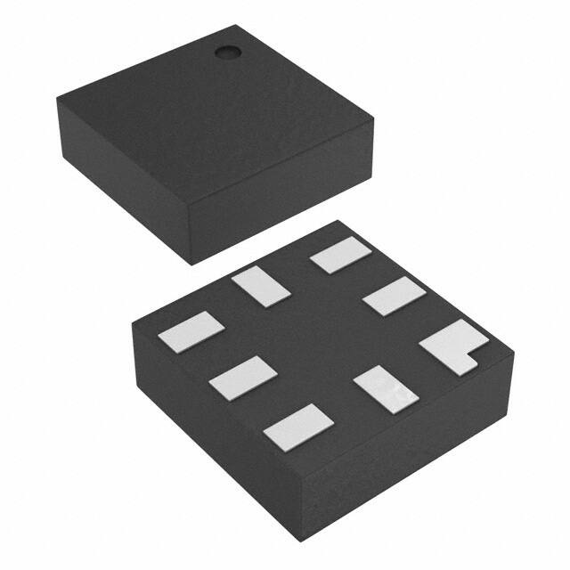
Packaged in MicroPak™ 8 (1.6mm x 1.6mm)
Applications
Mobile Phones
Alarm and Security Systems
IN(-) A
2
-
IN(+) A
3
+
1
Out A
Personal Digital Assistants
IN(-) B
IN(+) B
6
5
+
+
7
Out B
VSS
Figure 1. Functional Diagram
Ordering Information
Part Number Top Mark
FAN256L8X
CP
© 2010 Fairchild Semiconductor Corporation
FAN256 • Rev. 1.0.0
Operating
Temperature
Range
Package
Packing
Method
-40 to 85°C
8-Lead, MicroPak™ 1.6mm x 1.6mm Package
5000 Units on
Tape and Reel
www.fairchildsemi.com
FAN256 — Dual Low Voltage Comparator
May 2011
�FAN256 — Dual Low Voltage Comparator
Pin Configuration
OUT B
IN(-) B
7
IN(+) B
6
5
4
8
VDD
1
2
OUT A
VSS
3
IN(-) A IN(+) A
Figure 2. Pin Configuration (Top Through View)
Pin Definitions
Pin #
Name
Description
1
OUT A
Comparator A Output
2
IN(-) A
Inverting Input of Comparator A
3
IN(+) A
4
VSS
5
IN(+) B
Non-Inverting Input of Comparator B
6
IN(-) B
Inverting Input of Comparator B
7
OUT B
8
VDD
Non-Inverting Input of Comparator A
Negative Supply Voltage
Comparator B Output
Positive Supply Voltage
Function Table
Inputs
Outputs
IN(-) > IN(+)
Output LOW
IN(+) > IN(-)
Output HIGH
VDD
VOUT
VIN(-)
VDD
VOUT
VOUT
VOUT
VIN (+)
VIN (-)
VIN(+)
Figure 3. VIN vs. VOUT
© 2010 Fairchild Semiconductor Corporation
FAN256 • Rev. 1.0.0
www.fairchildsemi.com
2
�Stresses exceeding the absolute maximum ratings may damage the device. The device may not function or be
operable above the recommended operating conditions and stressing the parts to these levels is not recommended.
In addition, extended exposure to stresses above the recommended operating conditions may affect device reliability.
The absolute maximum ratings are stress ratings only.
Symbol
VDD to VSS
DVIN
VIN
Parameter
Condition
Supply Voltage
Max.
-3.0
+3.0
0
6.0
Differential Input Voltage
Unit
V
±6
Input Voltage
(1)
ts
Output Short Circuit Duration
TJ
Junction Temperature
TSTG
Min.
Storage Temperature Range
-65
VSS to VDD
V
Indefinite
S
+150
°C
+150
°C
PD
Power Dissipation
226
mW
JA
Thermal Resistance
287
°C/W
IEC 61000-4-2 System ESD
ESD
JEDEC JESD22-A114, Human Body
Model
JEDEC JESD22-C101, Charged
Device Model
Air Gap
15
Contact
8
All Pins
8
Pin to Pin: IN(-), IN(+)
to VDD or VSS
12
All Pins
2
FAN256 — Dual Low Voltage Comparator
Absolute Maximum Ratings
kV
Note:
1. The maximum total power dissipation must not be exceeded.
Recommended Operating Conditions
The Recommended Operating Conditions table defines the conditions for actual device operation. Recommended
operating conditions are specified to ensure optimal performance to the datasheet specifications. Fairchild does not
recommend exceeding them or designing to Absolute Maximum Ratings.
Symbol
VDD to VSS
Parameter
Power Supply
VDD
Power Supply
VIN
Input Voltage
IOH/IOL
Condition
Output Sink/Source Current
VSS=0V
Min.
Max.
-2.75
+2.75
0
5.5
1.6
© 2010 Fairchild Semiconductor Corporation
FAN256 • Rev. 1.0.0
5.5
V
V
5
VDD=3.0V
3
Operating Temperature, Free Air
V
VSS to VDD
VDD=5.0V
VDD=1.6V
TA
Unit
mA
1
-40
+85
°C
www.fairchildsemi.com
3
�Symbol
Parameter
Condition
Min.
Typ.
Max.
Unit
VDD=5.5V, VSS=GND, and TA=+25°C
VHYS
Input Hysteresis
VCM=0.5VDD
(2)
Input Offset Voltage
IIO
Input Offset Current
10
pA
II
Input Bias Current
10
pA
Common Mode Input Voltage
Common Mode Rejection Ratio(3)
IDD
Supply Current - Per Comparator
Power Supply Rejection Ratio
±1
VSS
CMRR
PSRR
-15
mV
VIO
VCM
VCM=0.5VDD
4
VDD
VCM=VDD
(3)
68
7
ΔVDD=0.5V
45
60
VO=VSS
90
Low-Level Output Voltage
ISINK=5.0mA
0.1
VOH
High-Level Output Voltage
ISOURCE=5.0mA
tPLH
Propagation Delay (Turn-On)
tPHL
Propagation Delay (Turn-Off)
Output Short Circuit Current
VOL
tTLH
tTHL
(4)
Response Time, Output Rise/Fall
5.2
mV
V
dB
17
80
VO=VDD
IOS
+15
µA
dB
mA
0.3
V
5.4
V
Overdrive=20mV,
CL=15pF
0.40
µs
Overdrive=20mV,
CL=15pF
0.42
µs
4.0
CL=50pF
FAN256 — Dual Low Voltage Comparator
Electrical Characteristics
ns
5.4
VDD=3V, VSS=GND, and TA=+25°C
VHYS
Input Hysteresis
VCM=0.5VDD
(2)
Input Offset Voltage
IIO
Input Offset Current
10
pA
II
Input Bias Current
10
pA
CMRR
IDD
PSRR
Common Mode Input Voltage
Common Mode Rejection Ratio
60
Supply Current(x) Per Comparator
Power Supply Rejection Ratio(3)
6
ΔVDD=0.5V
VO=VSS
35
ISINK=3.0mA
VOH
High-Level Output Voltage
ISOURCE=3.0mA
tPLH
Propagation Delay (Turn-On)
tPHL
Propagation Delay (Turn-Off)
(4)
0.15
V
15
µA
dB
mA
0.35
V
2.85
V
Overdrive=20mV,
CL=15pF
0.45
µs
Overdrive=20mV,
CL=15pF
0.47
µs
CL=50pF
2.65
mV
dB
70
27
Low-Level Output Voltage
Response Time, Output Rise/Fall
45
VO=VDD
VOL
+15
VDD
VCM=VDD
Output Short Circuit Current
tTHL
±1
VSS
(3)
IOS
tTLH
-15
mV
VIO
VCM
VCM=0.5VDD
4
6.1
6.2
ns
Continued on the following page…
© 2010 Fairchild Semiconductor Corporation
FAN256 • Rev. 1.0.0
www.fairchildsemi.com
4
�Symbol
Parameter
Condition
Min.
Typ.
Max.
Unit
VDD=1.6V, VSS=GND, and TA=+25°C
VHYS
Input Hysteresis
VIO
Input Offset Voltage
IIO
Input Offset Current
II
Input Bias Current
VCM
CMRR
IDD
PSRR
VCM=0.5VDD
(2)
VCM=0.5VDD
(3)
VCM=VDD
5.5
VO=VSS
7.5
Low-Level Output Voltage
ISINK=1.0mA
High-Level Output Voltage
ISOURCE=1.0mA
tPLH
Propagation Delay (Turn-On)
tPHL
Propagation Delay (Turn-Off)
(4)
Response Time, Output Rise/Fall
0.15
13
µA
dB
mA
0.25
V
1.50
V
Overdrive=20mV,
CL=15pF
0.52
µs
Overdrive=20mV,
CL=15pF
0.54
µs
CL=50pF
1.35
V
dB
70
VO=VDD
VOL
pA
56
45
mV
pA
VDD
5
ΔVDD=0.5V
VOH
tTHL
+15
10
Supply Current(x) Per Comparator
Output Short Circuit Current
±1
VSS
Power Supply Rejection Ratio(3)
IOS
tTLH
-15
mV
10
Common Mode Input Voltage
Common Mode Rejection Ratio
3.5
16.5
13.0
FAN256 — Dual Low Voltage Comparator
Electrical Characteristics
ns
Notes:
2. Differential input switching level is guaranteed at the minimum or maximum offset voltage, minus or plus half the
maximum hysteresis voltage.
3. Guaranteed by design and characterization data
4. Input signal: 1kHz, square-wave signal with 10ns edge rate.
© 2010 Fairchild Semiconductor Corporation
FAN256 • Rev. 1.0.0
www.fairchildsemi.com
5
�900
15.00
VDD=1.6V
800
14.00
VDD=3.0V
700
1.6 VDD
13.00
VDD=5.5V
600
3.0 VDD
500
5.5 VDD
ICC (µA)
IDD , Supply Current (µA)
16.00
12.00
11.00
400
300
10.00
200
9.00
100
0
8.00
-55 ⁰C
-40 ⁰C
Includes both Comparators
-25 ⁰C
25 ⁰C
85 ⁰C
0.01
95 ⁰C
0.1
1
Temp. =25C
CL = 15pF
TA, Ambient Temperature
Figure 4. Supply Current vs. Temperature
10
100
1000
Frequency (Khz)
Figure 5.
Supply Current vs. Output Transition
Frequency
6
FAN256 — Dual Low Voltage Comparator
Typical Performance Characteristics
5.5
VOH, Output Voltage HIGH State (V)
IDD, Supply Current (µA)
16
14
12
10
8
‐40 ⁰C
6
25 ⁰C
4
85 ⁰C
2
0
0
0.5
* Data includes
both comparators
1
1.5
2
2.5
3
3.5
4
4.5
5
5.5
6
5
4.5
4
3.5
3
2.5
2
VDD=1.6V
1.5
VDD=3.0V
1
V DD, Supply Voltage (V)
VDD=5.5V
0.5
0
2
4
6
8
10
ISOURCE, Output Source Current (mA)
Figure 6.
Supply Current vs. Supply Voltage
Figure 7. Output HIGH vs. Output Drive Current
380
360
340
100
320
tPHL (ns)
VOL , Output Voltage Low (mV)
400
1000
VDD=1.6V
10
300
280
VDD=3.0V
1.6VDD
260
VDD=5.5V
3.0VDD
240
5.5VDD
1
220
0.10
1.00
10.00
200
ISINK , Output Sink Current (mA)
-60
-40
-20
0
20
40
60
80
100
Temperature
Figure 8.
Figure 9. Propagation Delay (tPHL) vs. Temperature
Output LOW vs. Output Drive Current
© 2010 Fairchild Semiconductor Corporation
FAN256 • Rev. 1.0.0
www.fairchildsemi.com
6
�300
500
280
260
450
Delay (nS)
240
tPLH (ns)
400
350
300
220
200
180
1.6VDD
3.0VDD
160
tpLH
140
tpHL
120
250
5.5VDD
100
200
-60
-40
-20
0
20
40
60
80
0
100
Figure 10. Propagation Delay (tPLH)
vs. Temperature
100
150
200
250
Overdrive (mV)
Figure 11. Propagation Delay vs. Input Overdrive
3
2
TA = 25°C
7
6
1
5
Voltage (V)
Input Common Mode Voltage Range (V)
50
VDD=3.0V
Temp. =25°C
Temperature
FAN256 — Dual Low Voltage Comparator
Typical Performance Characteristics (Continued)
0
‐1
‐2
4
3
2
VDD
1
Output
0
‐3
0
1
2
3
4
5
6
50
100
Input Overdrive = 50mV
150
200
250
300
Time (µS)
Vs, Supply Voltage (V)
Figure 13. Power-Up Delay
Figure 12. Input Common Mode Voltage Range
vs. Supply Voltage
© 2010 Fairchild Semiconductor Corporation
FAN256 • Rev. 1.0.0
www.fairchildsemi.com
7
�FAN256 — Dual Low Voltage Comparator
Physical Dimensions
0.10
2X
C
A
1.6
B
1.6
INDEX AREA
0.10
2X
C
TOP VIEW
0.55 MAX
0.05
0.05
0.00
DETAIL A
8X(0.09)
C
8X
0.05
Recommended Landpattern
C
(0.20)
1.0
2
1
4 (0.1)
C
8
0.35
0.25
3X(0.2)
0.35
0.25
0.5
3
4
7
6
5
(0.15)
0.15 8X
0.25
0.10
0.05
C A B
C
0.35
0.25
DETAIL A
PIN #1 TERMINAL
SCALE: 2X
BOTTOM VIEW
Notes:
1. PACKAGE CONFORMS TO JEDEC MO-255 VARIATION UAAD
2. DIMENSIONS ARE IN MILLIMETERS
3. DRAWING CONFORMS TO ASME Y.14M-1994
4. PIN 1 FLAG, END OF PACKAGE OFFSET
5. DRAWING FILE NAME: MKT-MAC08AREV4
MAC08AREV4
Figure 14. 8-Lead, MicroPak™ 1.6mm Wide
Package drawings are provided as a service to customers considering Fairchild components. Drawings may change in any manner
without notice. Please note the revision and/or date on the drawing and contact a Fairchild Semiconductor representative to verify or
obtain the most recent revision. Package specifications do not expand the terms of Fairchild’s worldwide terms and conditions, specifically the
warranty therein, which covers Fairchild products.
Always visit Fairchild Semiconductor’s online packaging area for the most recent package drawings:
http://www.fairchildsemi.com/packaging/.
Tape and Reel Specifications
Please visit Fairchild Semiconductor’s online packaging area for the most recent tape and reel specifications:
hhttp://www.fairchildsemi.com/products/logic/pdf/micropak_tr.pdf/
© 2010 Fairchild Semiconductor Corporation
FAN256 • Rev. 1.0.0
www.fairchildsemi.com
8
�FAN256 — Dual Low Voltage Comparator
© 2010 Fairchild Semiconductor Corporation
FAN256 • Rev. 1.0.0
www.fairchildsemi.com
9
�
很抱歉,暂时无法提供与“FAN256L8X-F106”相匹配的价格&库存,您可以联系我们找货
免费人工找货