Is Now Part of
To learn more about ON Semiconductor, please visit our website at
www.onsemi.com
Please note: As part of the Fairchild Semiconductor integration, some of the Fairchild orderable part numbers
will need to change in order to meet ON Semiconductor’s system requirements. Since the ON Semiconductor
product management systems do not have the ability to manage part nomenclature that utilizes an underscore
(_), the underscore (_) in the Fairchild part numbers will be changed to a dash (-). This document may contain
device numbers with an underscore (_). Please check the ON Semiconductor website to verify the updated
device numbers. The most current and up-to-date ordering information can be found at www.onsemi.com. Please
email any questions regarding the system integration to Fairchild_questions@onsemi.com.
ON Semiconductor and the ON Semiconductor logo are trademarks of Semiconductor Components Industries, LLC dba ON Semiconductor or its subsidiaries in the United States and/or other countries. ON Semiconductor owns the rights to a number
of patents, trademarks, copyrights, trade secrets, and other intellectual property. A listing of ON Semiconductor’s product/patent coverage may be accessed at www.onsemi.com/site/pdf/Patent-Marking.pdf. ON Semiconductor reserves the right
to make changes without further notice to any products herein. ON Semiconductor makes no warranty, representation or guarantee regarding the suitability of its products for any particular purpose, nor does ON Semiconductor assume any liability
arising out of the application or use of any product or circuit, and specifically disclaims any and all liability, including without limitation special, consequential or incidental damages. Buyer is responsible for its products and applications using ON
Semiconductor products, including compliance with all laws, regulations and safety requirements or standards, regardless of any support or applications information provided by ON Semiconductor. “Typical” parameters which may be provided in ON
Semiconductor data sheets and/or specifications can and do vary in different applications and actual performance may vary over time. All operating parameters, including “Typicals” must be validated for each customer application by customer’s
technical experts. ON Semiconductor does not convey any license under its patent rights nor the rights of others. ON Semiconductor products are not designed, intended, or authorized for use as a critical component in life support systems or any FDA
Class 3 medical devices or medical devices with a same or similar classification in a foreign jurisdiction or any devices intended for implantation in the human body. Should Buyer purchase or use ON Semiconductor products for any such unintended
or unauthorized application, Buyer shall indemnify and hold ON Semiconductor and its officers, employees, subsidiaries, affiliates, and distributors harmless against all claims, costs, damages, and expenses, and reasonable attorney fees arising out
of, directly or indirectly, any claim of personal injury or death associated with such unintended or unauthorized use, even if such claim alleges that ON Semiconductor was negligent regarding the design or manufacture of the part. ON Semiconductor
is an Equal Opportunity/Affirmative Action Employer. This literature is subject to all applicable copyright laws and is not for resale in any manner.
�FAN3111 — Single 1A High-Speed, Low-Side
Gate Driver
Features
Description
1.4 A Peak Sink / Source at VDD = 12 V
The FAN3111 1A gate driver is designed to drive an Nchannel enhancement-mode MOSFET in low-side
switching applications.
Single Non-Inverting, Low-Voltage Input for
Compatibility with Low-Voltage Controllers
Small Footprint Facilitates Distributed Drivers for
Parallel Power Devices
15 ns Typical Delay Times
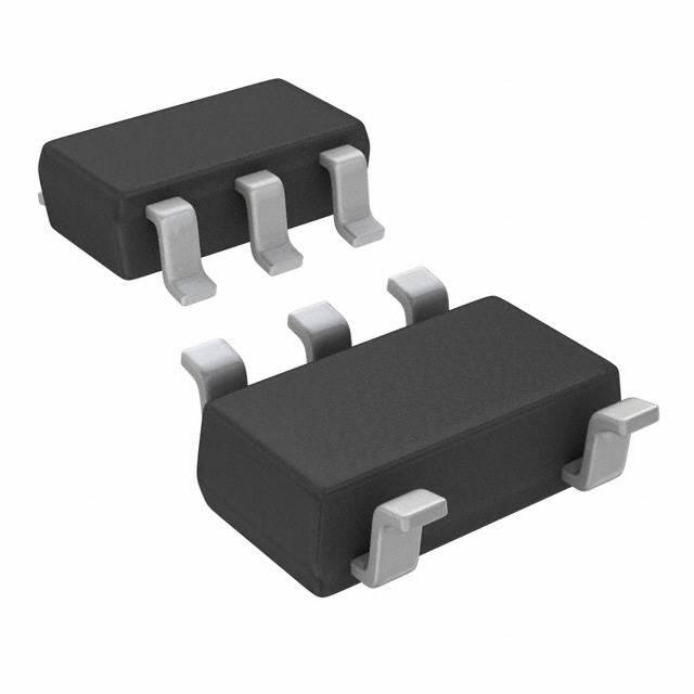
5-Pin SOT23 Package
1.1 A Sink / 0.9 A Source at VOUT = 6 V
4.5 to 18 V Operating Range
FAN3111C Compatible with FAN3100C Footprint
Two Input Configurations:
Dual CMOS Inputs Allow Configuration as
Non-Inverting or Inverting with Enable Function
Two input options are offered: FAN3111C has dual
CMOS inputs with thresholds referenced to VDD for use
with PWM controllers and other input-signal sources
that operate from the same supply voltage as the driver.
For use with low-voltage controllers and other inputsignal sources that operate from a lower supply voltage
than the driver, that supply voltage may also be used as
the reference for the input thresholds of the FAN3111E.
This driver has a single, non-inverting, low-voltage input
plus a DC input VXREF for an external reference voltage
in the range 2 to 5 V.
The FAN3111 is available in a lead-free finish industrystandard 5-pin SOT23.
9 ns Typical Rise / 8 ns Typical Fall times with
470 pF Load
Rated from –40°C to 125°C Ambient
Applications
Switch-Mode Power Supplies
Synchronous Rectifier Circuits
Pulse Transformer Driver
Logic to Power Buffer
Motor Control
VDD
1
GND
2
IN+
3
Figure 1.
5
4
OUT
IN−
FAN3111C (Top View)
© 2008 Fairchild Semiconductor Corporation
FAN3111 • Rev. 1.6
VDD
1
GND
2
IN+
3
Figure 2.
5
OUT
4
XREF
FAN3111E (Top View)
www.fairchildsemi.com
FAN3111 — Single 1A High-Speed, Low-Side Gate Driver
January 2015
�Part Number
Input
Threshold
Package
Packing Method
Quantity per
Reel
FAN3111CSX
CMOS
5-Pin SOT23
Tape & Reel
3,000
FAN3111ESX
External
5-Pin SOT23
Tape & Reel
3,000
Thermal Characteristics(1)
JL
Package
(2)
58
5-Pin SOT23
JT
(3)
102
JA
(4)
161
JB
(5)
53
JT
(6)
6
Units
°C/W
Notes:
1. Estimates derived from thermal simulation; actual values depend on the application.
2. Theta_JL (JL): Thermal resistance between the semiconductor junction and the bottom surface of all the leads
(including any thermal pad) that are typically soldered to a PCB.
3. Theta_JT (JT): Thermal resistance between the semiconductor junction and the top surface of the package,
assuming it is held at a uniform temperature by a top-side heatsink.
4. Theta_JA (ΘJA): Thermal resistance between junction and ambient, dependent on the PCB design, heat sinking,
and airflow. The value given is for natural convection with no heatsink using a 2S2P board,, as specified in
JEDEC standards JESD51-2, JESD51-5, and JESD51-7, as appropriate.
5. Psi_JB (JB): Thermal characterization parameter providing correlation between semiconductor junction
temperature and an application circuit board reference point for the thermal environment defined in Note 4. For
the MLP-8 package, the board reference is defined as the PCB copper connected to the thermal pad and
protruding from either end of the package. For the SOIC-8 package, the board reference is defined as the PCB
copper adjacent to pin 6.
6. Psi_JT (JT): Thermal characterization parameter providing correlation between the semiconductor junction
temperature and the center of the top of the package for the thermal environment defined in Note 4.
FAN3111 — Single 1A High-Speed, Low-Side Gate Driver
Ordering Information
Pin Definitions
Pin #
Name
1
VDD
Supply Voltage. Provides power to the IC.
2
GND
Ground. Common ground reference for input and output circuits.
3
IN+
Non-Inverting Input. Connect to VDD to enable output.
IN–
FAN3111C Inverting Input. Connect to GND to enable output.
4
5
Description
XREF
FAN3111E External Reference Voltage. Reference for input thresholds, 2 V to 5 V.
OUT
Gate Drive Output. Held low unless required inputs are present.
Output Logic with Dual-Input Configuration
IN+
IN−
OUT
0
(7)
0
0
0
(7)
(7)
0
1
0
1
1
(7)
0
1
1
Note:
7. Default input signal if no external connection is made.
© 2008 Fairchild Semiconductor Corporation
FAN3111 • Rev. 1.6
www.fairchildsemi.com
2
�IN+
1
VDD
5
OUT
2
GND
3
100kΩ
100kΩ
VDD
100kΩ
IN- 4
Figure 3.
FAN3111C Simplified Block Diagram
1
VDD
5
OUT
2
GND
FAN3111 — Single 1A High-Speed, Low-Side Gate Driver
Block Diagrams
XREF 4
IN+
3
100k
100k
Figure 4.
© 2008 Fairchild Semiconductor Corporation
FAN3111 • Rev. 1.6
FAN3111E Simplified Block Diagram
www.fairchildsemi.com
3
�Stresses exceeding the absolute maximum ratings may damage the device. The device may not function or be
operable above the recommended operating conditions and stressing the parts to these levels is not recommended.
In addition, extended exposure to stresses above the recommended operating conditions may affect device
reliability. The absolute maximum ratings are stress ratings only.
Symbol
Parameter
VDD
VDD to GND
VIN
Voltage on IN to GND
VXREF
Voltage on XREF to GND
VOUT
Voltage on OUT to GND
Min.
Max.
Unit
-0.3
20.0
V
FAN3111C
-0.3
VDD + 0.3
V
FAN3111E
-0.3
VXREF+0.3
V
FAN3111E
-0.3
5.5
V
-0.3
VDD+0.3
V
TL
Lead Soldering Temperature (10 Seconds)
+260
ºC
TJ
Junction Temperature
+150
ºC
TSTG
Storage Temperature
+150
ºC
-65
Recommended Operating Conditions
The Recommended Operating Conditions table defines the conditions for actual device operation. Recommended
operating conditions are specified to ensure optimal performance to the datasheet specifications. Fairchild does not
recommend exceeding them or designing to Absolute Maximum Ratings.
Symbol
Parameter
VDD
Supply Voltage Range
VIN
Input Voltage IN
VXREF
TA
External Reference Voltage XREF
Operating Ambient Temperature
© 2008 Fairchild Semiconductor Corporation
FAN3111 • Rev. 1.6
Min.
Max.
Unit
4.5
18.0
V
FAN3111C
0
VDD
V
FAN3111E
0
VXREF
V
FAN3111E
2.0
5.0
V
-40
+125
ºC
FAN3111 — Single 1A High-Speed, Low-Side Gate Driver
Absolute Maximum Ratings
www.fairchildsemi.com
4
�Unless otherwise noted, VDD = 12 V, VXREF = 3.3 V, TJ = -40°C to +125°C. Currents are defined as positive into the
device and negative out of the device.
Symbol
Parameter
Conditions
Min.
Typ.
Max.
Unit
18.0
V
10
µA
Supply
VDD
Operating Range
4.5
IDD
Static Supply Current
Inputs Not Connected
5
Inputs (FAN3111C)
VIL_C
IN Logic, Low-Voltage Threshold
VIH_C
IN Logic, High-Voltage Threshold
30
38
55
%VDD
70
%VDD
IINL
IN Current, Low
IN from 0 to VDD
-1
175
µA
IINH
IN Current, High
IN from 0 to VDD
-175
1
µA
VHYS_C
Input Hysteresis Voltage
17
%VDD
30
%VXREF
Inputs (FAN3111E)
VIL_E
IN Logic, Low-Voltage Threshold
VIH_E
IN Logic, High-Voltage Threshold
25
50
60
%VXREF
IINL
IN Current, Low
IN from 0 to VXREF
-1
50
µA
IINH
IN Current, High
IN from 0 to VXREF
-50
1
µA
VHYS_E
Input Hysteresis Voltage
20
%VXREF
OUT at VDD/2,
CLOAD = 47nF, f = 1KHz
1.1
A
OUT at VDD/2,
CLOAD = 47nF, f = 1KHz
-0.9
A
CLOAD = 47nF, f = 1KHz
1.4
A
CLOAD = 47nF, f = 1KHz
-1.4
A
FAN3111 — Single 1A High-Speed, Low-Side Gate Driver
Electrical Characteristics
Output
ISINK
OUT Current, Mid-Voltage, Sinking
(8)
ISOURCE
OUT Current, Mid-Voltage, Sourcing
IPK_SINK
OUT Current, Peak, Sinking
(8)
IPK_SOURCE OUT Current, Peak, Sourcing
tRISE
tFALL
tD1, tD2
Output Rise Time
Output Fall Time
(8)
(8)
(9)
(9)
Output Prop. Delay
CLOAD = 470pF
9
18
ns
CLOAD = 470pF
8
17
ns
15
30
ns
FAN3111C: 0 - 12VIN,
1V/ns Slew Rate
(9)
FAN3111E: 0 - 3.3VIN,
1V/ns Slew Rate
IRVS
Output Reverse Current Withstand
(8)
250
mA
Notes:
8. Not tested in production.
9. See Timing diagrams.
© 2008 Fairchild Semiconductor Corporation
FAN3111 • Rev. 1.6
www.fairchildsemi.com
5
�90%
90%
Output
Output
10%
10%
VINH
IN+
VINH
VINL
IN -
tD1
tRISE
Figure 5.
tD1
tFALL
tD2
tRISE
tFALL
Non-Inverting Waveforms
© 2008 Fairchild Semiconductor Corporation
FAN3111 • Rev. 1.6
VINL
tD2
Figure 6.
Inverting Waveforms
FAN3111 — Single 1A High-Speed, Low-Side Gate Driver
Timing Diagrams
www.fairchildsemi.com
6
�Typical characteristics are provided at 25°C, VDD = 12 V, and VXREF = 3.3 V unless otherwise noted.
2.5
2.5
2.0
IDD (μA)
IDD (μA)
FAN3111E
FAN3111C
2.0
1.5
1.0
1.5
1.0
Inputs Floating, Output Low
Inputs Floating, Output Low
0.5
0.5
0.0
0.0
4
6
8
10
12
14
16
4
18
6
8
Supply Voltage (V)
2.0
2.0
1.8
1.8
1.6
1.6
1.4
1.4
1.2
1.2
1.0
1.0
0.8
0.8
0.6
0.6
0.4
0.4
0.2
0.2
0.0
0.0
IDD (Static) vs. Supply Voltage
FAN3111C
FAN3111C
Figure 8.
1.8
1.6
V DD = 15V
V DD = 12V
V DD = 8V
V
V DD = 4.5V
200
200
Figure 9.
400
400
FAN3111E
1.4
1.2
1.0
7
600
600
800
800
V DD = 4.5V
0
200
Figure 10.
9
V DD = 15V
600
800
1000
IDD (No-Load) vs. Frequency
FAN3111E
8
7
V DD = 4.5V
4
3
2
2
1
1
0
V DD = 8 V
5
3
V DD = 15 V
V DD = 12 V
6
IDD (mA)
IDD (mA)
400
Sw itching Frequency (kHz)
V DD = 8V
4
V DD = 15V
V DD = 8V
1000
1000
V DD = 12V
5
18
V DD = 12V
0.8
0.6
0.4
IDD (No-Load) vs. Frequency
FAN3111C
6
16
IDD (Static) vs. Supply Voltage
Sw
Sw itching
itching Frequency
Frequency (kHz)
(kHz)
8
14
0.2
0.0
00
9
12
Supply Voltage (V)
IDD (mA)
(mA)
IIDD
DD (mA)
Figure 7.
10
FAN3111 — Single 1A High-Speed, Low-Side Gate Driver
Typical Performance Characteristics
V DD = 4.5 V
0
0
200
400
600
800
1000
0
200
Sw itching Frequency (kHz)
Figure 11.
600
800
1000
Sw itching Frequency (kHz)
IDD (470pF Load) vs. Frequency
© 2008 Fairchild Semiconductor Corporation
FAN3111 • Rev. 1.6
400
Figure 12.
IDD (470pF Load) vs. Frequency
www.fairchildsemi.com
7
�Typical characteristics are provided at 25°C, V DD = 12 V, and VXREF = 3.3 V unless otherwise noted.
3
3
FAN3111C
FAN3111E
2
IDD (μA)
IDD (μA)
2
Inputs Floating, Output Low
1
0
-50
-25
0
Figure 13.
25
50
75
Tem perature (°C)
100
0
-50
125
IDD (Static) vs. Temperature
25
50
75
Tem perature (°C)
100
125
IDD (Static) vs. Temperature
FAN3111E
8
7
Input Thresholds (V)
FAN3111C
V IH
6
5
4
3
2
V IL
V IH
2.0
1.5
1.0
V IL
0.5
4
6
Figure 15.
8
10
12
14
Supply Voltage (V)
16
2.5
18
Input Thresholds vs. Supply Voltage
3.0
Figure 16.
3.5
4.0
XREF (V)
4.5
5.0
Input Threshold vs. XREF Voltage
7.0
100%
90%
80%
70%
60%
50%
40%
30%
20%
10%
0%
FAN3111C
FAN3111C
Input Thresholds (V)
DD)
0
Figure 14.
1
0
Input Thresholds (% of V
-25
2.5
10
9
Input Thresholds (V)
Inputs Floating, Output Low
1
FAN3111 — Single 1A High-Speed, Low-Side Gate Driver
Typical Performance Characteristics
VIH
V IL
4
6
8
10
12
14
16
6.5
5.5
5.0
V IL
4.5
4.0
-50
18
V IH
6.0
-25
Supply Voltage (V)
Figure 17.
Input Thresholds % vs. Supply Voltage
© 2008 Fairchild Semiconductor Corporation
FAN3111 • Rev. 1.6
Figure 18.
0
25
50
75
Tem perature (°C)
100
125
Input Threshold vs. Temperature
www.fairchildsemi.com
8
�Typical characteristics are provided at 25°C, V DD = 12 V, and VXREF = 3.3 V unless otherwise noted.
2.0
70
Propagation Delays (ns)
Input Thresholds (V)
FAN3111E
1.8
1.6
V IH
1.4
1.2
V IL
1.0
50
40
IN rise to OUT fall
30
20
IN fall to OUT
10
0
0.8
-50
-25
Figure 19.
0
25
50
75
Tem perature (°C)
100
4
125
Input Threshold vs. Temperature
6
Figure 20.
8
10
12
14
Supply Voltage (V)
Propagation Delays (ns)
70
FAN3111C Non-Inverting Input
60
50
40
IN Fall to OUT Fall
30
20
10
IN Rise to OUT Rise
18
Propagation Delay vs. Supply Voltage
4
6
8
10
FAN3111E
80
70
60
50
IN Fall to OUT Fall
40
30
20
10
IN Rise to OUT Rise
0
0
12
14
16
4
18
6
8
Supply Voltage (V)
Figure 21.
Propagation Delay vs. Supply Voltage
Figure 22.
12
14
16
18
Propagation Delay vs. Supply Voltage
20
FAN3111E
FAN3111C Non-Inverting Input
Propagation Delays (ns)
22
10
Supply Voltage (V)
24
Propagation Delays (ns)
16
90
80
Propagation Delays (ns)
FAN3111C Inverting Input
60
FAN3111 — Single 1A High-Speed, Low-Side Gate Driver
Typical Performance Characteristics
20
IN Fall to OUT Fall
18
16
14
12
10
-50
Figure 23.
IN Rise to OUT Rise
-25
0
25
50
75
Tem perature (°C)
100
16
IN Fall to OUT Fall
14
12
10
8
-50
125
Propagation Delay vs. Temperature
© 2008 Fairchild Semiconductor Corporation
FAN3111 • Rev. 1.6
18
IN Rise to OUT Rise
-25
Figure 24.
0
25
50
75
Tem perature (°C)
100
125
Propagation Delays vs. Temperature
www.fairchildsemi.com
9
�Typical characteristics are provided at 25°C, V DD = 12 V, and VXREF = 3.3 V unless otherwise noted.
120
FAN3111C Inverting Input
CL = 4.7nF
20
100
Fall Time (ns)
Propagation Delays (ns)
22
IN Rise to OUT Fall
18
16
14
IN Fall to OUT Rise
12
80
60
CL = 2.2nF
40
CL = 1.0nF
CL = 470pF
20
10
-50
0
-25
0
25
50
75
100
125
0
5
10
Tem perature (°C)
Figure 25.
20
Supply Voltage (V)
Propagation Delays vs. Temperature
Figure 26.
Fall Time vs. Supply Voltage
12
140
Rise and Fall Times (ns)
CL = 4.7nF
120
Rise Time (ns)
15
100
80
60
CL = 2.2nF
40
CL = 1.0nF
20
CL = 470pF
0
0
5
10
15
20
CL = 470pF
11
Rise Tim e
10
9
Fall Tim e
8
7
-50
-25
Supply Voltage (V)
Figure 27.
Rise Time vs. Supply Voltage
FAN3111 — Single 1A High-Speed, Low-Side Gate Driver
Typical Performance Characteristics
Figure 28.
0
25
50
75
Tem perature (°C)
100
125
Rise and Fall Time vs. Temperature
VDD = 12V
CL = 470 pF
tRISE = 9 ns
IOUT (0.5A /div)
VOUT (5V/div)
tFALL = 8 ns
VOUT (5V / div)
VIN (5V/div)
(CMOS Input)
VIN (2V/div)
(3.3V Input)
t = 20ns/div
Figure 29.
Rise and Fall Waveforms (470pF)
© 2008 Fairchild Semiconductor Corporation
FAN3111 • Rev. 1.6
Figure 30.
CLOAD = 47 nF
t = 100ns / div
Quasi-Static Source Current (VDD=12V)
www.fairchildsemi.com
10
�Typical characteristics are provided at 25°C, V DD = 12 V, and VXREF = 3.3 V unless otherwise noted.
IOUT (0.5A /div)
IOUT (0.5A /div)
VOUT (5V / div)
VOUT (5V / div)
CLOAD = 47 nF
t = 100ns / div
VIN (2V/div)
(3.3V Input)
Figure 31.
VIN (2V/div)
(3.3V Input)
Quasi-Static Sink Current (VDD=12V)
Figure 32.
CLOAD = 47 nF
t = 100ns / div
Quasi-Static Source Current (VDD=8V)
V DD
IOUT (0.5A /div)
4.7µF
Ceram ic
470µF
A l. E l.
Current Probe
LECROY AP015
FAN3111
FAN3111 — Single 1A High-Speed, Low-Side Gate Driver
Typical Performance Characteristics
VOUT (5V / div)
I OUT
VIN (2V/div)
(3.3V Input)
Figure 33.
IN
1kHz
CLOAD = 47 nF
V OU T
C LOAD
47nF
t = 100ns / div
Quasi-Static Sink Current (VDD=8V)
© 2008 Fairchild Semiconductor Corporation
FAN3111 • Rev. 1.6
1µF
Ceram ic
Figure 34.
Quasi-Static IOUT / VOUT Test Circuit
www.fairchildsemi.com
11
�The FAN3111 offers CMOS- or logic-level-compatible
input thresholds. In the FAN3111C, the logic input
thresholds are dependent on the V DD level and, with VDD
of 12 V, the logic rising-edge threshold is approximately
55% of VDD and the input falling-edge threshold is
approximately 38% of VDD. The CMOS input
configuration
offers
a
hysteresis
voltage
of
approximately 17% of VDD. The CMOS inputs can be
used with relatively slow edges (approaching DC) if
good decoupling and bypass techniques are
incorporated in the system design to prevent noise from
violating the input-voltage hysteresis window. This
allows setting precise timing intervals by fitting an R-C
circuit between the controlling signal and the IN pin of
the driver. The slow rising edge at the IN pin of the
driver introduces a delay between the controlling signal
and the OUT pin of the driver.
Figure 36 illustrates startup operation as VDD increases
from 0 to 12 V with the output commanded to the high
level (IN+ tied to VDD, IN- tied to GND). This
configuration might not be suitable for driving high-side
P-channel MOSFETs because the low output voltage of
the driver would attempt to turn the P-channel MOSFET
on with low VDD levels.
VDD
OUT
OUT @ 5 V/Div
FAN3111C
VDD @ 5 V/Div
In the FAN3111E, the input thresholds are dependent
on the VXREF voltage that typically is chosen between 2V
and 5 V. This range of VXREF allows compatibility with
TTL and other logic levels up to 5 V by connecting the
XREF pin to the same source as the logic circuit that
drives the FAN3111E input stage. The logic rising edge
threshold is approximately 50% of VXREF and the input
falling-edge threshold is approximately 30% of VXREF.
The TTL-like input configuration offers a hysteresis
voltage of approximately 20% of VXREF.
t = 200 us/Div
Figure 36.
Startup Operation as VDD Increases
Figure 37 illustrates FAN3111E startup operation with the
output commanded to the low level (IN+ tied to ground)
and the voltage on XREF ramped from 0 to 3.3 V.
VDD
Startup Operation
XREF
OUT
The FAN3111 internal logic is optimized to drive ground
referenced N-channel MOSFETs as VDD supply voltage
rises during startup operation. As VDD rises from 0V to
approximately 2 V, the OUT pin is held LOW by an
internal resistor, regardless of the state of the input
pins. When the internal circuitry becomes active at
approximately 2 V, the output assumes the state
commanded by the inputs.
FAN3111E
OUT @ 2 V/Div
VXREF @ 2 V/Div
t = 50 us/Div
Figure 35 illustrates FAN3111C startup operation with
VDD increasing from 0 to 12 V, with the output
commanded to the low level (IN+ and IN- tied to
ground). Note that OUT is held LOW to maintain an Nchannel MOSFET in the OFF state.
Figure 37.
FAN3111
drivers
incorporate
the
MillerDrive
architecture shown in Figure 38 for the output stage, a
combination of bipolar and MOS devices capable of
providing large currents over a wide range of supplyvoltage and temperature variations. The bipolar devices
carry the bulk of the current as OUT swings between
1/3 to 2/3 VDD and the MOS devices pull the output to
the high or low rail.
OUT
FAN3111C
OUT @ 5 V/Div
The purpose of the MillerDrive architecture is to speed
up switching by providing the highest current during the
Miller plateau region when the gate-drain capacitance of
the MOSFET is being charged or discharged as part of
the turn-on / turn-off process. For applications with zero
voltage switching during the MOSFET turn-on or turn-off
interval, the driver supplies high peak current for fast
switching even though the Miller plateau is not present.
This situation often occurs in synchronous rectifier
applications because the body diode is generally
conducting before the MOSFET is switched on.
VDD @ 5 V/Div
t = 200 us/Div
FAN3111C Startup Operation
© 2008 Fairchild Semiconductor Corporation
FAN3111 • Rev. 1.6
FAN3111E Startup Operation
MillerDrive™ Gate Drive Technology
VDD
Figure 35.
VDD @ 5 V/Div
FAN3111 — Single 1A High-Speed, Low-Side Gate Driver
Applications Information
www.fairchildsemi.com
12
�
Keep the driver as close to the load as possible to
minimize the length of high-current traces. This
reduces the series inductance to improve highspeed switching, while reducing the loop area that
can radiate EMI to the driver inputs and other
surrounding circuitry.
Many high-speed power circuits can be susceptible
to noise injected from their own output or other
external sources, possibly causing output retriggering. These effects can be especially obvious
if the circuit is tested in breadboard or non-optimal
circuit layouts with long input, enable, or output
leads. For best results, make connections to all
pins as short and direct as possible.
The turn-on and turn-off current paths should be
minimized as discussed in the following sections.
VDD
Input
stage
Figure 38.
VOUT
Figure 39 shows the pulsed gate-drive current path
when the gate driver is supplying gate charge to turn
the MOSFET on. The current is supplied from the local
bypass capacitor, CBYP, and flows through the driver to
the MOSFET gate and to ground. To reach the high
peak currents possible, the resistance and inductance
in the path should be minimized. The localized CBYP
acts to contain the high peak-current pulses within this
driver-MOSFET circuit, preventing them from disturbing
the sensitive analog circuitry in the PWM controller.
MillerDrive™ Output Architecture
VDD Bypass Capacitor Guidelines
To enable this IC to turn a power device on quickly, a
local, high-frequency, bypass capacitor CBYP with low
ESR and ESL should be connected between the VDD
and GND pins with minimal trace length. This capacitor
is in addition to bulk electrolytic capacitance of 10 µF to
47 µF often found on driver and controller bias circuits.
VDD
A typical criterion for choosing the value of CBYP is to
keep the ripple voltage on the VDD supply ≤5%. Often
this is achieved with a value ≥ 20 times the equivalent
load capacitance CEQV, defined here as Qgate/VDD.
Ceramic capacitors of 0.1 µF to 1 µF or larger are
common choices, as are dielectrics, such as X5R and
X7R, which have good temperature characteristics and
high pulse current capability.
CBYP
FAN3111
PWM
Figure 39.
If circuit noise affects normal operation, the value of
CBYP may be increased to 50-100 times the CEQV or
CBYP may be split into two capacitors. One should be a
larger value, based on equivalent load capacitance, and
the other a smaller value, such as 1-10 nF, mounted
closest to the VDD and GND pins to carry the higherfrequency components of the current pulses.
Current Path for MOSFET Turn-On
Figure 40 shows the current path when the gate driver
turns the MOSFET off. Ideally, the driver shunts the
current directly to the source of the MOSFET in a small
circuit loop. For fast turn-off times, the resistance and
inductance in this path should be minimized.
VDD
Layout and Connection Guidelines
FAN3111
PWM
Keep high-current output and power ground paths
separate from logic input signals and signal ground
paths. This is especially critical when dealing with
TTL-level logic thresholds.
© 2008 Fairchild Semiconductor Corporation
FAN3111 • Rev. 1.6
VDS
CBYP
The FAN3111 incorporates fast reacting input circuits,
short propagation delays, and output stages capable of
delivering current peaks over 1 A to facilitate voltage
transition times from under 10 ns to over 100 ns. The
following layout and connection guidelines are strongly
recommended:
VDS
FAN3111 — Single 1A High-Speed, Low-Side Gate Driver
The output-pin slew rate is determined by VDD voltage
and the load on the output. It is not user adjustable, but
if a slower rise or fall time at the MOSFET gate is
needed, a series resistor can be added.
Figure 40.
Current Path for MOSFET Turn-Off
www.fairchildsemi.com
13
�Thermal Guidelines
The FAN3111 truth table indicates the operational
states using the dual-input configuration. In a noninverting driver configuration, the IN- pin should be a
logic low signal. If the IN- pin is connected to logic high,
a disable function is realized, and the driver output
remains low regardless of the state of the IN+ pin.
Gate drivers used to switch MOSFETs and IGBTs at
high frequencies can dissipate significant amounts of
power. It is important to determine the driver power
dissipation and the resulting junction temperature in the
application to ensure that the part is operating within
acceptable temperature limits.
Table 1. FAN3111 Truth Table
The total power dissipation in a gate driver is the sum of
three components; PGATE, PQUIESCENT, and PDYNAMIC:
IN+
IN-
OUT
0
0
0
0
1
0
1
0
1
1
1
0
Ptotal Pgate PDynamic
Gate Driving Loss: The most significant power loss
results from supplying gate current (charge per unit
time) to switch the load MOSFET on and off at the
switching frequency. The power dissipation that results
from driving a MOSFET at a specified gate-source
voltage, VGS, with gate charge, QG, at switching
frequency, fSW , is determined by:
In the non-inverting driver configuration in Figure 41,
the IN- pin is tied to ground and the input signal (PWM)
is applied to the IN+ pin. The IN- pin can be connected
to logic high to disable the driver and the output
remains low, regardless of the state of the IN+ pin.
PGATE QG VGS fsw
IN+
IN-
FAN3111
OUT
PDYNAMIC IDYNAMIC VDD
GND
Figure 41.
TJ PTOTAL JL TC
where:
TJ = driver junction temperature;
θJL = thermal resistance from junction to lead; and
TL = lead temperature of device in application.
In the inverting driver application shown in Figure 42, the
IN+ pin is tied high. Pulling the IN+ pin to GND forces the
output low, regardless of the state of the IN- pin.
PWM
Figure 42.
IN-
ROUT,Driver
PPKG PTOTAL
ROUT,DRIVER REXT RGATE,FET (5)
where:
PPKG = power dissipated in the driver package;
ROUT,DRIVER = estimated driver impedance derived from
IOUT vs. VOUT waveforms;
REXT = external series resistance connected between
the driver output and the gate of the MOSFET; and
RGATE,FET = resistance internal to the load MOSFET gate
and source connections.
OUT
GND
Dual-Input Driver Enabled, Inverting
Configuration
© 2008 Fairchild Semiconductor Corporation
FAN3111 • Rev. 1.6
(4)
The power dissipated in a gate-drive circuit is
independent of the drive-circuit resistance and is split
proportionately among the resistances present in the
driver, any discrete series resistor present, and the gate
resistance internal to the power switching MOSFET.
Power dissipated in the driver may be estimated using
the following equation:
VDD
FAN3111
(3)
Once the power dissipated in the driver is determined,
the driver junction temperature rise with respect to the
device lead can be evaluated using thermal equation:
Dual-Input Driver Enabled, NonInverting Configuration
IN+
(2)
Dynamic Pre-drive / Shoot-through Current: A power loss
resulting from internal current consumption under
dynamic operating conditions, including pin pull-up /
pull-down resistors, can be obtained using the graphs in
Figure 11 and Figure 12 in Typical Performance
Characteristics to determine the current IDYNAMIC drawn
from VDD under actual operating conditions:
VDD
PWM
(1)
FAN3111 — Single 1A High-Speed, Low-Side Gate Driver
Truth Table of Logic Operation
www.fairchildsemi.com
14
�Rectified
AC Input
VDD
Downstream
Converters
Q1A
33W
FAN3111
Logic
PWM
VDD
Q1B
33W
FAN3111
Figure 43.
PFC Boost Circuit Utilizing Distributed Drivers for Parallel Power Switches Q1A and Q1B
VIN
VDD
PWM
FAN3111 — Single 1A High-Speed, Low-Side Gate Driver
Typical Application Diagrams
FAN3111
Figure 44.
Driver for Forward Converter Low-Side Switch
Q1
VIN
T2
T1
D1
VSEC
D2
VDD
Q2
CC
PWM
FAN3111
0.1µF
Figure 45.
© 2008 Fairchild Semiconductor Corporation
FAN3111 • Rev. 1.6
Driver for Two-Transistor, Forward-Converter Gate Transformer
www.fairchildsemi.com
15
�Part
Number
Type
Gate
(10)
Drive
(Sink/Src)
Input
Threshold
FAN3111C Single 1A +1.1 A /-0.9 A CMOS
FAN3111E
Single 1A +1.1 A /-0.9 A External(11)
Logic
Package
Single Channel of Dual-Input/Single-Output
SOT23-5
Single Non-Inverting Channel with External
Reference
SOT23-5
FAN3100C Single 2A
+2.5A / -1.8A
CMOS
Single Channel of Two-Input/One-Output
SOT23-5, MLP6
FAN3100T
+2.5A / -1.8A
TTL
Single Channel of Two-Input/One-Output
SOT23-5, MLP6
FAN3226C Dual 2A
+2.4A / -1.6A
CMOS
Dual Inverting Channels + Dual Enable
SOIC8, MLP8
FAN3226T
Dual 2A
+2.4A / -1.6A
TTL
Dual Inverting Channels + Dual Enable
SOIC8, MLP8
FAN3227C Dual 2A
+2.4A / -1.6A
CMOS
Dual Non-Inverting Channels + Dual Enable
SOIC8, MLP8
FAN3227T
Dual 2A
+2.4A / -1.6A
TTL
Dual Non-Inverting Channels + Dual Enable
SOIC8, MLP8
FAN3228C Dual 2A
+2.4A / -1.6A
CMOS
Dual Channels of Two-Input/One-Output, Pin Config.1
SOIC8, MLP8
FAN3228T
Dual 2A
+2.4A / -1.6A
TTL
Dual Channels of Two-Input/One-Output, Pin Config.1
SOIC8, MLP8
FAN3229C Dual 2A
+2.4A / -1.6A
CMOS
Dual Channels of Two-Input/One-Output, Pin Config.2
SOIC8, MLP8
FAN3229T
Dual 2A
+2.4A / -1.6A
TTL
Dual Channels of Two-Input/One-Output, Pin Config.2
SOIC8, MLP8
FAN3268T
Dual 2A
+2.4A / -1.6A
TTL
18V Half-Bridge Driver: Non-Inverting Channel (NMOS)
and Inverting Channel (PMOS) + Dual Enables
SOIC8
FAN3223C Dual 4A
+4.3A / -2.8A
CMOS
Dual Inverting Channels + Dual Enable
SOIC8, MLP8
FAN3223T
Dual 4A
+4.3A / -2.8A
TTL
Dual Inverting Channels + Dual Enable
SOIC8, MLP8
FAN3224C Dual 4A
+4.3A / -2.8A
CMOS
Dual Non-Inverting Channels + Dual Enable
SOIC8, MLP8
FAN3224T
Dual 4A
+4.3A / -2.8A
TTL
Dual Non-Inverting Channels + Dual Enable
SOIC8, MLP8
FAN3225C Dual 4A
+4.3A / -2.8A
CMOS
Dual Channels of Two-Input/One-Output
SOIC8, MLP8
FAN3225T
+4.3A / -2.8A
TTL
Dual Channels of Two-Input/One-Output
SOIC8, MLP8
FAN3121C Single 9A
+9.7A / -7.1A
CMOS
Single Inverting Channel + Enable
SOIC8, MLP8
FAN3121T
Single 9A
+9.7A / -7.1A
TTL
Single Inverting Channel + Enable
SOIC8, MLP8
FAN3122T
Single 9A
+9.7A / -7.1A
CMOS
Single Non-Inverting Channel + Enable
SOIC8, MLP8
FAN3122C Single 9A
+9.7A / -7.1A
TTL
Single Non-Inverting Channel + Enable
SOIC8, MLP8
Single 2A
Dual 4A
FAN3111 — Single 1A High-Speed, Low-Side Gate Driver
Table 2. Related Products
Notes:
10. Typical currents with OUT at 6V and VDD = 12V.
11. Thresholds proportional to an externally supplied reference voltage.
© 2008 Fairchild Semiconductor Corporation
FAN3111 • Rev. 1.6
www.fairchildsemi.com
16
��ON Semiconductor and
are trademarks of Semiconductor Components Industries, LLC dba ON Semiconductor or its subsidiaries in the United States and/or other countries.
ON Semiconductor owns the rights to a number of patents, trademarks, copyrights, trade secrets, and other intellectual property. A listing of ON Semiconductor’s product/patent
coverage may be accessed at www.onsemi.com/site/pdf/Patent−Marking.pdf. ON Semiconductor reserves the right to make changes without further notice to any products herein.
ON Semiconductor makes no warranty, representation or guarantee regarding the suitability of its products for any particular purpose, nor does ON Semiconductor assume any liability
arising out of the application or use of any product or circuit, and specifically disclaims any and all liability, including without limitation special, consequential or incidental damages.
Buyer is responsible for its products and applications using ON Semiconductor products, including compliance with all laws, regulations and safety requirements or standards,
regardless of any support or applications information provided by ON Semiconductor. “Typical” parameters which may be provided in ON Semiconductor data sheets and/or
specifications can and do vary in different applications and actual performance may vary over time. All operating parameters, including “Typicals” must be validated for each customer
application by customer’s technical experts. ON Semiconductor does not convey any license under its patent rights nor the rights of others. ON Semiconductor products are not
designed, intended, or authorized for use as a critical component in life support systems or any FDA Class 3 medical devices or medical devices with a same or similar classification
in a foreign jurisdiction or any devices intended for implantation in the human body. Should Buyer purchase or use ON Semiconductor products for any such unintended or unauthorized
application, Buyer shall indemnify and hold ON Semiconductor and its officers, employees, subsidiaries, affiliates, and distributors harmless against all claims, costs, damages, and
expenses, and reasonable attorney fees arising out of, directly or indirectly, any claim of personal injury or death associated with such unintended or unauthorized use, even if such
claim alleges that ON Semiconductor was negligent regarding the design or manufacture of the part. ON Semiconductor is an Equal Opportunity/Affirmative Action Employer. This
literature is subject to all applicable copyright laws and is not for resale in any manner.
PUBLICATION ORDERING INFORMATION
LITERATURE FULFILLMENT:
Literature Distribution Center for ON Semiconductor
19521 E. 32nd Pkwy, Aurora, Colorado 80011 USA
Phone: 303−675−2175 or 800−344−3860 Toll Free USA/Canada
Fax: 303−675−2176 or 800−344−3867 Toll Free USA/Canada
Email: orderlit@onsemi.com
© Semiconductor Components Industries, LLC
N. American Technical Support: 800−282−9855 Toll Free
USA/Canada
Europe, Middle East and Africa Technical Support:
Phone: 421 33 790 2910
Japan Customer Focus Center
Phone: 81−3−5817−1050
www.onsemi.com
1
ON Semiconductor Website: www.onsemi.com
Order Literature: http://www.onsemi.com/orderlit
For additional information, please contact your local
Sales Representative
www.onsemi.com
�


 工商网监
湘ICP备2023018690号
工商网监
湘ICP备2023018690号

