Microphone Pre-Amplifier
with Digital Output
FAN3852
Description
The FAN3852 integrates a pre−amplifier, LDO, and ADC that
converts Electret Condenser Microphone (ECM) outputs to digital
Pulse Density Modulation (PDM) data streams. The pre−amplifier
accepts analog signals from the ECM and drives an over−sampled
sigma delta Analog−to−Digital Converter (ADC) and outputs PDM
data. The PDM digital audio has the advantage of noise rejection and
easy interface to mobile handset processors.
The FAN3852 features an integrated LDO and is powered from the
system supply rails up to 3.63 V, with low power consumption of only
0.85 mW and less than 20 mW in Power−Down Mode.
www.onsemi.com
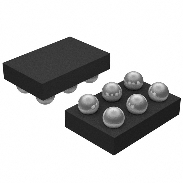
WLCSP−6
CASE 567TS
Features
• Optimized for Mobile Handset and Notebook PC Microphone
•
•
•
•
•
•
•
•
•
•
•
•
Applications
Accepts Input from Electret Condenser Microphones (ECM)
Pulse Density Modulation (PDM) Output
Standard 5−Wire Digital Interface
Low Input Capacitance, High PSR, 20 kHz Pre−Amplifier
Low−Power 1.5 mA Sleep Mode
Typical 420 mA Supply Current
SNR of 62 dB (A) for 16 dB Gain
Total Harmonic Distortion 0.02%
Input Clock Frequency Range of 1−4 MHz
Integrated Low Drop−Out Regulator (LDO)
Small 1.242 mm × 0.842 mm 6−Ball, 0.400 mm pitch standard
WLCSP Package
1.5 kV HBM ESD on MIC Input
A1
A2
SELECT
GND
B1
B2
INPUT
DATA
C1
C2
VDD
Top View
PIN CONFIGURATION
MARKING DIAGRAM
VK&K
&.&2&Z
Pin A1
Typical Applications
•
•
•
•
CLOCK
Electret Condenser Microphones with Digital Output
Mobile Handset
Headset Accessories
Personal Computer (PC)
VK
K
.
2
Z
= Device Identifier
= Lot Run Code
= Pin A1 Mark
= Date Code
= Plant Code
ORDERING INFORMATION
See detailed ordering and shipping information on page 2
of this data sheet.
© Semiconductor Components Industries, LLC, 2016
June, 2021 − Rev. 4
1
Publication Order Number:
FAN3852/D
�FAN3852
ORDERING INFORMATION
Part Number
Operating Temperature Range
Package
Packing Method†
FAN3852UC16X
−40°C to 85°C
6 Ball, Wafer−Level
Chip−Scale Package (WLCSP)
3000 Units/Tape & Reel
†For information on tape and reel specifications, including part orientation and tape sizes, please refer to our Tape and Reel Packaging
Specifications Brochure, BRD8011/D.
INTERNAL BLOCK DIAGRAM
VDD
Sleep
Mode Ctrl
LDO
CLOCK
INPUT
S−D
ADC
Pre*Amp
DATA
SELECT
GND
Figure 1. Block Diagram
Table 1. PIN DEFINITIONS
Pin #
Name
Type
A1
CLOCK
Input
Clock Input
Description
B1
GND
Input
Ground Pin
C1
DATA
Output
A2
SELECT
Input
Rising or Falling Clock Edge Select
B2
INPUT
Input
Microphone Input
C2
VDD
Input
Device Power Pin
PDM Output − 1 Bit ADC
Table 2. ABSOLUTE MAXIMUM RATINGS
Symbol
Parameter
Min.
Max.
Unit
VDD
DC Supply Voltage
−0.3
4.0
V
VIO
Digital I/O
−0.3
VDD + 0.3
V
Microphone Input
−0.3
2.2
ESD
Human Body Model, JESD22−A114, All Pins Except Microphone
Input
Human Body Model, JESD2−A114 − Microphone Input
±8
kV
±1.5
Stresses exceeding those listed in the Maximum Ratings table may damage the device. If any of these limits are exceeded, device functionality
should not be assumed, damage may occur and reliability may be affected.
1. This device is fabricated using CMOS technology and is therefore susceptible to damage from electrostatic discharges. Appropriate
precautions must be taken during handling and storage of this device to prevent exposure to ESD.
www.onsemi.com
2
�FAN3852
Table 3. RELIABILITY INFORMATION
Rating
Symbol
TJ
Typ.
Junction Temperature
TSTG
Storage Temperature Range
TRFLW
Peak Reflow Temperature
qJA
Min.
−65
Thermal Resistance, JEDEC Standard, Multilayer
Test Boards, Still Air
Max.
Unit
+150
°C
+125
°C
+260
°C
90
°C/W
2. TA = 25°C unless otherwise specified
Table 4. RECOMMENDED OPERATING CONDITIONS
Rating
Symbol
TA
VDD
TRF−CLK
Min.
Operating Temperature Range
−40
Supply Voltage Range
1.64
Typ.
Max.
Unit
+85
°C
3.63
V
10
ns
1.80
Clock Rise and Fall Time
Functional operation above the stresses listed in the Recommended Operating Ranges is not implied. Extended exposure to stresses beyond
the Recommended Operating Ranges limits may affect device reliability.
Table 5. DEVICE SPECIFIC ELECTRICAL CHARACTERISTICS
FAN3852UC16X
SNR
Min.
Value
Symbol
Signal−to−Noise Ratio
fIN = 1 kHz (1 Pa), A−Weighted
Typ.
Max.
Unit
62
eN
Total Input RMS Noise
20 Hz to 20 kHz, A−Weighted
VIN
Maximum Input Signal
fIN = 1 kHz, THD + N < 10%, Level = 0 V
dB (A)
5.74
6.80
mVRMS
448
mVPP
3. Guaranteed by characterization and/or design. Not production tested.
Table 6. ELECTRICAL CHARACTERISTICS
Unless otherwise specified, al limits are guaranteed for TA = 25°C, VDD = 1.8 V, VIN = 94 dB (SPL) and fCLK = 2.4 MHz.
Duty Cycle = 50% and CMIC = 15 pF
Symbol
Parameter
Condition
Min.
Typ.
Max.
Unit
1.64
1.80
3.63
V
VDD
Supply Voltage Range
IDD
Supply Current
INPUT = AC Coupled to GND,
CLOCK = On, No Load
420
Sleep Mode Current
fCLK = GND
1.50
Power Supply Rejection (Note 5)
INPUT = AC Coupled to GND,
Test Signal on VDD = 217 Hz,
Square Wave and Broadband
Noise (Note 4), Both 100 mVP−P
−74
dBFS
Nominal Sensitivity (Note 6)
INPUT = 94 dBSPL (1 Pa)
−26
dBFS
Total Harmonic Distortion (Note 7)
fIN = 1 KHz, INPUT = −26 dBFS
0.02
0.20
%
THD and Noise (Note 5)
50 Hz ≤ fIN ≤ 1 kHz,
INPUT = −20 dBFS
0.2
1.0
%
fIN = 1 KHz, INPUT = −5 dBFS
1.0
5.0
10.0
ISLEEP
PSR
INNOM
THD
THD+N
fIN = 1 KHz, INPUT = 0 dBFS
5.0
CIN
Input Capacitance (Note 8)
INPUT
1.3
RIN
Input Resistance (Note 8)
INPUT
VIL
CLOCK & SELECT Input Logic
LOW Level
mA
8.0
pF
>10
GW
0.3
www.onsemi.com
3
mA
V
�FAN3852
Table 6. ELECTRICAL CHARACTERISTICS (continued)
Unless otherwise specified, al limits are guaranteed for TA = 25°C, VDD = 1.8 V, VIN = 94 dB (SPL) and fCLK = 2.4 MHz.
Duty Cycle = 50% and CMIC = 15 pF
Symbol
Parameter
VIH
CLOCK & SELECT Input Logic
HIGH Level
VOL
Data Output Logic LOW Level
VOH
Data Output Logic HIGH Level
VOUT
Condition
Min.
Typ.
1.5
Max.
Unit
VDD+0.3
V
0.35*VDD
V
0.65*VDD
V
Acoustic Overload Point (Note 8)
THD+N < 10%
120
tA
Time from CLOCK Transition to
Data becoming Valid
On Falling Edge of CLOCK,
SELECT = GND, CLOAD = 15 pF
18
43
tB
Time from CLOCK Transition to
Data becoming HIGH−Z
On Rising Edge of CLOCK,
SELECT = GND, CLOAD = 15 pF
0
5
tA
Time from CLOCK Transition to
Data becoming Valid
On Rising Edge of CLOCK,
SELECT = VDD, CLOAD = 15 pF
18
58
tB
Time from CLOCK Transition to
Data becoming HIGH−Z
On Falling Edge of CLOCK,
SELECT = VDD, CLOAD = 15 pF
0
5
16
ns
Input CLOCK Frequency (Note 9)
Active Mode
1.0
2.4
4.0
MHz
40
50
60
%
0.35
2.00
ms
0.01
1.00
ms
100
pF
fCLK
CLKdc
tWAKEUP
CLOCK Duty Cycle (Note 5)
Wake−Up Time (Note 10)
fCLK = 2.4 MHz
tFALLASLEAP
Fall−Asleep Time (Note 11)
fCLK = 2.4 MHz
CLOAD
Load Capacitance on Data
0
dBSPL
ns
16
ns
ns
Product parametric performance is indicated in the Electrical Characteristics for the listed test conditions, unless otherwise noted. Product
performance may not be indicated by the Electrical Characteristics if operated under different conditions.
4. Pseudo−random noise with triangular probability density function. Bandwidth up to 10 MHz.
5. Guaranteed by characterization. Not production tested.
6. Assuming that 120 dB (SPL) is mapped to 0 dBFS.
7. Assuming an input of −45 dBV.
8. Guaranteed by design. Not production tested.
9. All parameters are tested at 2.4 MHz. Frequency range guaranteed by characterization.
10. Device wakes up when fCLK ≥ 300 kHz.
11. Device falls asleep when fCLK ≤ 70 kHz.
CLK
Data
Valid
DATA1
tA
HIGH−Z
tB
DATA2
(For possible 2nd Mic)
Data
Valid
HIGH−Z
tA
tA − Microphone delay from clock edge to data assertion.
tB − Microphone delay from clock edge to high−impedance state.
tA > tB to have interim HIGH−Z state in both signals.
Figure 2. Interface Timing
www.onsemi.com
4
�FAN3852
TYPICAL PERFORMANCE CHARACTERISTICS
Unless otherwise specified, all limits are guaranteed for TA = 25°C, VDD = 1.8 V, VIN = 94 dB (SPL), fCLK = 2.4 MHz and duty Cycle = 50%.
Amplitude Spectrum [dBFS], Fo = 1000.2135 Hz, Fs = 2.400000 MHz, SNR = 56.89 dB, SNR = 60.88 dB(A), THD = 0.008 %
Noise
Noise(A)
Signal
−20
THD = 81.95 dB
SNR = 60.88 dBc(A)
SINAD = 56.87 dB
ENOB = 13.50
N = 2097152 pts
Blackman Window
← Fo(0)= −26.15 dBFS
−40
Amplitude [dBFS]
−60
−80
−100
↓ Integrated Noise = −87.03 dBFS(A)
Spur = −101.34 dBFS, SFDR = 75.19 dBc
↓
← Fo(1)= −110.28 dBFS
← Fo(2)= −116.40 dBFS
−120
← Fo(3)= −120.45 dBFS
← Fo(4)= −125.03 dBFS
−140
−160
10 1
102
103
104
Frequency [Hz]
Figure 3. Noise vs. Frequency
Figure 4. THD, SINDA, and SNR vs. Input Amplitude
www.onsemi.com
5
105
106
�FAN3852
TYPICAL PERFORMANCE CHARACTERISTICS (continued)
Unless otherwise specified, all limits are guaranteed for TA = 25°C, VDD = 1.8 V, VIN = 94 dB (SPL), fCLK = 2.4 MHz and duty Cycle = 50%.
Figure 5. THD, SINAD and SNR vs. Output Level
4
3
Delta (dB)
−40
0.1971
−30
−20
−10
0
10
20
25
30
40
50
60
70
80
85
0.1644
0.1260
0.0954
0.0657
0.0359
0.0139
0.0000
−0.0097
−0.0344
−0.0514
−0.0739
−0.0998
−0.1183
−0.1271
2
ΔGain (dB)
Temp (°C)
1
0
-1
-2
-3
-4
-40
-30 -20 -10
0
10
20
30
40
50
Junction Temperature- Tj ˚C
Figure 6. � Gain vs. Temperature (Nominal Temperature = 255C)
www.onsemi.com
6
60
70
80
�FAN3852
APPLICATIONS INFORMATION
VDD
Audio
Output
SPEAKER
CLOCK
INPUT
Pre *
Amp
ADC
DATA
SELECT
CLK SDI SDO L/R
Low Pass Filter
Decimation
Serial Port
Noise Shaper
Interpolation
Applications Software
Figure 7. Mono Microphone Application Circuit
VDD
Audio
Output
SPEAKER
CLOCK
INPUT
Pre *
Amp
ADC
DATA
SELECT
VDD
CLOCK
INPUT
Pre *
Amp
ADC
CLK SDI SDO L/R
Serial Port
Low Pass Filter
Noise Shaper
Decimation
Interpolation
Applications Software
DATA
SELECT
Figure 8. Stereo Microphone Application Circuit
www.onsemi.com
7
�FAN3852
APPLICATIONS INFORMATION (continued)
Diaphragm
Airgap
Electret
Backplate
INPUT
FAN3852
V DD
CLOCK
DATA
SELECT
GND
Figure 9. MIC Element Drawing
A 0.1 mF decoupling capacitor is required for VDD. It can
be located inside the microphone or on the PCB very close
to the VDD pin.
Due to high input impedance, care should be taken to
remove all flux used during the reflow soldering process.
A 100 W resistance is recommended on the clock output
of the device driving the FAN3852 to minimize ringing and
improve signal integrity.
For optimal PSR, route a trace to the VDD pin. Do not
place a VDD plane under the device.
1.64 V − 3.63 V
C2
C3
RBIAS
2.2 k
VDD
SELECT
CLOCK
C1
+
DATA
INPUT
1−4 MHz
PDM Clock
PDM Data
PDM
Codec
GND
ECM
U1
FAN3852
Figure 10. Example Hardware Implementation
Table 7. RECOMMENDED COMPONENTS
Ref Des
Qty
Description of Options
Package
Manufacturer
Mfg PIN
U1
1
FAN3852 Microphone Pre−Amplifier
with Digital Output
WLCSP6
ON
Semiconductor
FAN3852UC16X
C1
1
Input AC Coupling Capacitor;
1 nF/1000 pF, ≥ 6.3 V, low−leakage
0402
Johansen
Dielectrics
500R07W102KV4T
0402
Murata
GCM155R71H102KA37D
0603
Taiyo Yuden
UMK107SD102KA−T
0402
Samsung
CL05B104KO5NNNC
0402
Yageo
CC0402KRX7R7BB104
0603
AVX
06033C104KAT4A
0402
Samsung
CL05B103KB5VPNC
0402
Murata
GCM155R71H103KA55J
0603
Yageo
CC0603KRX7R7BB103
C2
C3
1
1
Primary VDD Decoupling Capacitor;
0.1 mF, MLCC, ≥ 6.3 V
Optional VDD Decoupling Capacitor;
0.01 mF, MLCC, ≥ 6.3 V
www.onsemi.com
8
�MECHANICAL CASE OUTLINE
PACKAGE DIMENSIONS
WLCSP6 1.242x0.842x0.457
CASE 567TS
ISSUE A
DOCUMENT NUMBER:
DESCRIPTION:
98AON13367G
DATE 06 JUN 2019
Electronic versions are uncontrolled except when accessed directly from the Document Repository.
Printed versions are uncontrolled except when stamped “CONTROLLED COPY” in red.
WLCSP6 1.242x0.842x0.457
PAGE 1 OF 1
ON Semiconductor and
are trademarks of Semiconductor Components Industries, LLC dba ON Semiconductor or its subsidiaries in the United States and/or other countries.
ON Semiconductor reserves the right to make changes without further notice to any products herein. ON Semiconductor makes no warranty, representation or guarantee regarding
the suitability of its products for any particular purpose, nor does ON Semiconductor assume any liability arising out of the application or use of any product or circuit, and specifically
disclaims any and all liability, including without limitation special, consequential or incidental damages. ON Semiconductor does not convey any license under its patent rights nor the
rights of others.
© Semiconductor Components Industries, LLC, 2018
www.onsemi.com
�onsemi,
, and other names, marks, and brands are registered and/or common law trademarks of Semiconductor Components Industries, LLC dba “onsemi” or its affiliates
and/or subsidiaries in the United States and/or other countries. onsemi owns the rights to a number of patents, trademarks, copyrights, trade secrets, and other intellectual property.
A listing of onsemi’s product/patent coverage may be accessed at www.onsemi.com/site/pdf/Patent−Marking.pdf. onsemi reserves the right to make changes at any time to any
products or information herein, without notice. The information herein is provided “as−is” and onsemi makes no warranty, representation or guarantee regarding the accuracy of the
information, product features, availability, functionality, or suitability of its products for any particular purpose, nor does onsemi assume any liability arising out of the application or use
of any product or circuit, and specifically disclaims any and all liability, including without limitation special, consequential or incidental damages. Buyer is responsible for its products
and applications using onsemi products, including compliance with all laws, regulations and safety requirements or standards, regardless of any support or applications information
provided by onsemi. “Typical” parameters which may be provided in onsemi data sheets and/or specifications can and do vary in different applications and actual performance may
vary over time. All operating parameters, including “Typicals” must be validated for each customer application by customer’s technical experts. onsemi does not convey any license
under any of its intellectual property rights nor the rights of others. onsemi products are not designed, intended, or authorized for use as a critical component in life support systems
or any FDA Class 3 medical devices or medical devices with a same or similar classification in a foreign jurisdiction or any devices intended for implantation in the human body. Should
Buyer purchase or use onsemi products for any such unintended or unauthorized application, Buyer shall indemnify and hold onsemi and its officers, employees, subsidiaries, affiliates,
and distributors harmless against all claims, costs, damages, and expenses, and reasonable attorney fees arising out of, directly or indirectly, any claim of personal injury or death
associated with such unintended or unauthorized use, even if such claim alleges that onsemi was negligent regarding the design or manufacture of the part. onsemi is an Equal
Opportunity/Affirmative Action Employer. This literature is subject to all applicable copyright laws and is not for resale in any manner.
PUBLICATION ORDERING INFORMATION
LITERATURE FULFILLMENT:
Email Requests to: orderlit@onsemi.com
onsemi Website: www.onsemi.com
◊
TECHNICAL SUPPORT
North American Technical Support:
Voice Mail: 1 800−282−9855 Toll Free USA/Canada
Phone: 011 421 33 790 2910
Europe, Middle East and Africa Technical Support:
Phone: 00421 33 790 2910
For additional information, please contact your local Sales Representative
�