FAN5602
Universal
(Step-Up/Step-Down) Charge
Pump Regulated DC/DC
Converter
www.onsemi.com
Description
The FAN5602 is a universal switched capacitor DC/DC converter
capable of step−up or step−down operation. Due to its unique adaptive
fractional switching topology, the device achieves high efficiency over
a wider input/ output voltage range than any of its predecessors. The
FAN5602 utilizes resistance−modulated loop control, which produces
lower switching noise than other topologies. Depending upon actual
load conditions, the device automatically switches between
constant−frequency and pulse−skipping modes of operation to extend
battery life.
The FAN5602 produces a fixed regulated output within the range of
2.7 V to 5.5 V from any type of voltage source. High efficiency is
achieved under various input/ output voltage conditions because an
internal logic circuit automatically reconfigures the system to the best
possi− ble topology. Only two 1 mF bucket capacitors and one 10 mF
output capacitor are needed. During power on, soft−start circuitry
prevents excessive current drawn from the supply. The device is
protected against short−circuit and over−temperature conditions.
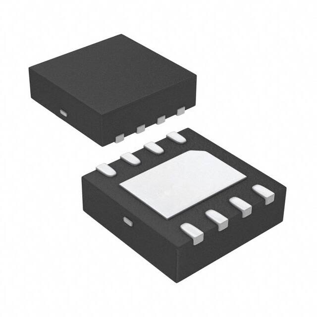
The FAN5602 is available with 4.5 V and 5.0 V output voltages in a
3x3 mm WDFN8 package.
1
WDFN8 3x3, 0.65P
CASE 511CD
MARKING DIAGRAM
602
ALYWG
G
602 = Specific Device Code
A
= Assembly Location
L
= Wafer Lot
Y
= Year
W = Work Week
G
= Pb−Free Package
(Note: Microdot may be in either location)
Features
•
•
•
•
•
•
•
•
•
•
•
•
•
•
•
Low−Noise, Constant−Frequency Operation at Heavy Load
High−Efficiency, Pulse−Skip (PFM) Operation at Light Load
Switch Configurations (1:3, 1:2, 2:3, 1:1, 3:2, 2:1, 3:1)
92% Peak Efficiency
Input Voltage Range: 2.7 V to 5.5 V
Output Current: 4.5 V, 100 mA at VIN = 3.6 V
±3% Output Voltage Accuracy
ICC < 1 mA in Shutdown Mode
1 MHz Operating Frequency
Shutdown Isolates Output from Input
Soft−Start Limits Inrush Current at Startup
Short−Circuit and Over−Temperature Protection
Minimum External Component Count
No Inductors
This is a Pb−Free Device
PIN ASSIGNMENTS
VIN
1
8
ENABLE
C2+
2
7
C1+
3
6
VOUT
4
5
C1−
C2−
GND
3x3mm 8−Lead MLP
ORDERING INFORMATION
See detailed ordering and shipping information on page 2
of this data sheet.
Applications
• Cell Phones
• Handheld Computers
• Portable RF Communication Equipment
© Semiconductor Components Industries, LLC, 2019
July, 2019 − Rev. 0
• Core Supply to Low−Power Processors
• Low−Voltage DC Bus
• DSP Supplies
1
Publication Order Number:
FAN604P/D
�FAN5602
ORDERING INFORMATION
Part Number
Output Voltage, NVOM
Package
Packing Method†
FAN5602MP45X
4.5 V
WDFN8 3x3, 0.65P (Pb−Free)
3000 / Tape & Reel
FAN5602MP5X
5.0 V
WDFN8 3x3, 0.65P (Pb−Free)
3000 / Tape & Reel
†For information on tape and reel specifications, including part orientation and tape sizes, please refer to our Tape and Reel Packaging
Specifications Brochure, BRD8011/D
Application Diagram
Input 2.7V to 5.5V
VIN
ENABLE
1
C2+
CIN
CB
C2−
GND
2
FAN5602
8
6
3
7
4
5
VOUT
C1+
COUT
C1−
Figure 1. Typical Application Diagram
Block Diagram
VIN
ENABLE
C1−
C1+
BAND GAP
VOUT
FB
ERROR
AMP
SOFT−START
BG
Light load
FB
EN
S
W
I
T
C
H
Heavy Load
CURRENT
SENSE
EN
C2 +
PFM
BG
R
A
Y
VIN
MODE
150mV
VOUT
SC
CONTROL LOGIC
REF
DRIVER
C2−
1.6V
VIN
UVLO
OSCILLATOR
GND
VIN
V OUT
Figure 2. Block Diagram
www.onsemi.com
2
�FAN5602
Pin Assignments
VIN
1
8
ENABLE
C2+
2
7
C1+
C2−
3
6
VOUT
GND
4
5
C1−
3x3mm 8−Lead MLP
Figure 3. Pin Assignments
Table 1. PIN DESCRIPTIONS
Pin #
Name
Description
1
VIN
Supply Voltage Input.
2
C2+
Bucket Capacitor2. Positive Connection.
3
C2−
Bucket Capacitor2. Negative Connection.
4
GND
Ground
5
C1−
Bucket Capacitor1. Negative Connection.
6
VOUT
7
C1+
8
ENABLE
Regulated Output Voltage. Bypass this pin with 10 mF ceramic low−ESR capacitor.
Bucket Capacitor1. Positive Connection.
Enable Input. Logic high enables the chip and logic low disables the chip, reducing the supply current to
less than 1 mA. Do not float this pin.
Table 2. ABSOLUTE MAXIMUM RATINGS
Symbol
VIN
Parameter
Min
Max
Unit
VIN, VOUT, ENABLE, Voltage to GND
−3.0
6.0
V
Voltage at C1+,C1−,C2+, and C2−to GND
−3.0
VIN + 0.3
V
PD
Power Dissipation
TL
Lead Soldering Temperature (10 seconds)
300
°C
TJ
Junction Temperature
150
°C
TSTG
Storage Temperature
150
°C
Human Body Model (HBM)
2
kV
Charged Device Model (CDM)
2
kV
ESD
Internally Limited
−55
Stresses exceeding those listed in the Maximum Ratings table may damage the device. If any of these limits are exceeded, device functionality
should not be assumed, damage may occur and reliability may be affected.
1. Using Mil Std. 883E, method 3015.7 (Human Body Model) and EIAJ/JESD22C101−A (Charged Device Model).
Table 3. RECOMMENDED OPERATING CONDITIONS
Symbol
Parameter
VIN
Input Voltage
IL
Load Current
TA
Condition
Min
1.8
Typ
Max
Unit
5.5
V
VIN < 2 V
30
4.5 & 5.5,VIN = 3.6 V
100
mA
Ambient Temperature
−40
+85
°C
Functional operation above the stresses listed in the Recommended Operating Ranges is not implied. Extended exposure to stresses beyond
the Recommended Operating Ranges limits may affect device reliability.
2. Refer to Figure 9 in Typical Performance Characteristics
www.onsemi.com
3
�FAN5602
Table 4. DC ELECTRICAL CHARACTERISTICS
VIN = 2.7 V to 5.5 V, C1 = C2 = 1 mF, CIN = COUT = 10 mF, ENABLE = VIN, TA = −40°C to +85°C unless otherwise noted. Typical values are
at TA = 25°C.
Symbol
Parameter
VUVLO
Input Under−Voltage Lockout
VOUT
Output Voltage
VIN ≥ 0.75 x VNOM, 0 mA < ILOAD < 100 mA
Quiescent Current
IQ
Condition
Min
Typ
Max
Unit
1.5
1.7
2.2
v
0.97 x VNOM
VNOM
1.03 x VNOM
V
VIN ≥ 1.1 x VNOM, ILOAD = 0 mA
170
300
mA
Off Mode Supply Current
ENABLE = GND
0.1
1.0
mA
Output Short−Circuit
VOUT < 150 mV
200
mA
Efficiency
VIN = 0.85 x VNOM, ILOAD =
30 mA
4.5, 5.0 V
80
VIN = 1.1 x VNOM, ILOAD =
30 mA
4.5, 5.0 V
92
%
fOSC
Oscillator Frequency
TSD
Thermal Shutdown Threshold
145
°C
TSDHYS
Thermal Shutdown Threshold
Hysteresis
15
°C
TA = 25°C
0.7
1.0
1.3
MHz
VIH
ENABLE Logic Input High
Voltage
VIL
ENABLE Logic Input Low
Voltage
IEN
ENABLE Logic Input Bias
Current
ENABLE =VIN or GND
tON
VOUT Turn−On Time
VIN = 0.9 x VNOM, ILOAD = 0 mA,10% to
90%
0.5
ms
VOUT Ripple
VIN = 2.5 V, ILOAD = 200 mA
10
mVpp
1.5
V
−1
0.5
V
1
mA
Product parametric performance is indicated in the Electrical Characteristics for the listed test conditions, unless otherwise noted. Product
performance may not be indicated by the Electrical Characteristics if operated under different conditions.
www.onsemi.com
4
�FAN5602
TYPICAL PERFORMANCE CHARACTERISTICS
180
80
160
70
140
60
Shutdown Current (nA)
Quiescent Current (μA)
TA = 25°C, VOUT = 4.5 V unless otherwise noted.
120
100
80
60
40
50
40
30
20
10
20
0
0
1.5
2.5
3.5
4.5
1
5.5
2
3
4
5
6
Input Voltage (V)
Input Voltage (V)
Figure 4. Quiescent Current vs. Input Voltage
Figure 5. Shutdown Current vs. Input Voltage
100
4.55
90
80
ILOAD = 100mA
VOUT = 4.5V
4.45
Efficiency
Output Voltage (V)
4.50
4.40
70
60
50
Load Current = 10mA
Load Current = 50mA
Load Current = 100mA
Load Current = 150mA
40
4.35
30
20
2.500
4.30
2.0
2.5
3.0
3.5
4.0
4.5
5.0
5.5
6.0
3.000
3.500
Input Voltage (V)
4.500
5.000
5.500
Figure 7. Efficiency vs. Input Voltage
Figure 6. Line Regulation
700.0
4.6
600.0
4.5
VIN = 3.6V
Load Current (mA)
Output Voltage (V)
4.000
Input Voltage
4.4
4.3
4.2
4.1
DVOUT < 10%
DVOUT < 3%
500.0
400.0
300.0
200.0
100.0
0.0
4.0
1
50
100
150
200
250
300
2
350
Load Currrent (mA)
2.5
3
3.5
4
4.5
5
Input Voltage (V)
Figure 8. Load Regulation
Figure 9. Output Current Capacity vs. Input voltage
www.onsemi.com
5
�FAN5602
4.5
5
Load Current = 10mA
Output Voltage (V)
Output Voltage (V)
4.5
4
3.5
3
Load Current = 10mA
Load Current = 50mA
Load Current = 100mA
Load Current = 150mA
Load Current = 200mA
2.5
4.45
4.4
4.35
4.3
2
2
3
4
5
−60 −40 −20
6
0
Input Voltage (V)
20
40
60
80
100
120
140
Ambient Temperature (C)
Figure 10. Output Voltage vs. Input Voltage
Figure 11. Output Voltage vs. Ambient Temperature
1.4
80
1.3
1.2
VIN = 3.6V
Enable (V)
Efficiency (%)
75
70
1.1
1
65
0.9
60
0.8
0
50
100
150
200
250
300
2
Mode Change Threshold (V)
5.5
Mode 1
4.5
Mode 2
4
3.5
3
Mode 3
2.5
Mode 4
2
0
50
100
150
3
3.5
4
4.5
5
5.5
6
Figure 13. Enable Threshold vs. Input Voltage
Figure 12. Peak Efficiency vs. Load Current
5
2.5
200
Load Current (mA)
Figure 14. Mode Change Threshold and Hysteresis
www.onsemi.com
6
�FAN5602
TYPICAL PERFORMANCE CHARACTERISTICS (Continued)
TA = 25°C, CIN = COUT = 10 mF, CB = 1 mF, VOUT = 4.5 V unless otherwise noted.
IOUT = 200mA
VIN = 2.5V
VIN = 3.6V
Output Ripple
(20 mV/div)
Output Ripple
(20 mV/div)
IOUT = 200mA
Time (100 μs/div)
Time (100 μs/div)
Figure 15. Output Ripple
Figure 16. Output Ripple
IOUT = 200mA
IOUT = 300mA
VIN = 4.2V
Output Ripple
(20 mV/div)
Output Ripple
(20 mV/div)
VIN = 2.5V
Time (100 μs/div)
Time (100 μs/div)
Figure 17. Output Ripple
Figure 18. Output Ripple
IOUT = 300mA
VIN = 3.6V
VIN = 4.2V
Output Ripple
(20 mV/div)
Output Ripple
(20 mV/div)
IOUT= 300mA
Time (100 μs/div)
Time (100 μs/div)
Figure 19. Output Ripple
Figure 20. Output Ripple
www.onsemi.com
7
�FAN5602
FUNCTIONAL DESCRIPTION
to a half of the input voltage. In pumping phase, the flying
capacitors are placed in parallel. The input is connected to
the bottom the capacitors so that the top of the capacitors is
boosted to a voltage that equals VIN/2 + VIN, i.e., 3/2 x VIN.
By connecting the top of the capacitors to the output, one can
ideally charge the output to 3/2 x VIN. If 3/2 x VIN is higher
than the needed VOUT, the linear regulation loop adjusts the
on− resistance to drop some voltage. Boosting the voltage of
the top of the capacitors to 3/2 x VIN by connecting VIN the
bottom of the capacitors, boosts the power efficiency 3/2
times. In 2:3 mode, the ideal power efficiency is VOUT/1.5 x
VIN. For example, if VIN = 2 V, VOUT = 2 x VIN = 4 V, the ideal
power efficiency is 100%.
When 2 x VIN > VOUT > 1.5 x VIN, the 1:2 mode (step−up)
shown in Figure 23 is used. Both in the charging phase and
in pumping phase, two flying capacitors are placed in
parallel. In charging phase, the capacitors are charged to the
input voltage. In the pumping phase, the input volt− age is
placed to the bottom of the capacitors. The top of the
capacitors is boosted to 2 x VIN. By connecting the top of the
capacitors to the output, one can ideally charge the output to
2 x VIN. Boosting the voltage on the top of the capacitors to
2VIN boosts the power efficiency 2 times. In 1:2 mode, the
ideal power efficiency is VOUT/2 x VIN. For example, VIN =
2V, VOUT = 2 x VIN = 4V, the ideal power efficiency is 100%.
When 3 x VIN > VOUT > 2 x VIN, the 1:3 mode (step−up)
shown in Figure 24 is used. In charging phase, two flying
capacitors are placed in parallel and each is charged to VIN.
In the pumping phase, the two flying capacitors are placed
in series and the input is connected to the bottom of the series
connected capacitors. The top of the series connected
capacitors is boosted to 3 x VIN. The ideal power efficiency
is boosted 3 times and is equal to VOUT/ 3VIN. For example,
VIN = 1 V, VOUT = 3 x VIN = 3 V, the ideal power efficiency is
100%. By connecting the output to the top of the series
connected capacitors, one can charge the output to 3 x VIN.
The internal logic in the FAN5602 monitors the input and
the output compares them, and automatically selects the
switch configuration to achieve the highest efficiency.
The step−down modes 3:2, 2:1, and 3:1 can be under−
stood by reversing the function of VIN and VOUT in the above
discussion.
The built−in modes improve power efficiency and extend
the battery life. For example, if VOUT = 5 V, mode 1:2 needs
a minimum VIN = 2.5 V. By built−in 1:3 mode, the minimum
battery voltage is extended to 1.7 V.
FAN5602 is a high−efficiency, low−noise switched
capacitor DC/DC converter capable of step−up and
step−down operations. It has seven built−in switch
configurations. Based on the ratio of the input voltage to the
output volt− age, the FAN5602 automatically reconfigures
the switch to achieve the highest efficiency. The regulation
of the output is achieved by a linear regulation loop, which
modulates the on−resistance of the power transistors so that
the amount of charge transferred from the input to the flying
capacitor at each clock cycle is controlled and is equal to the
charge needed by the load. The current spike is reduced to
minimum. At light load, the FAN5602 automatically
switches to Pulse Frequency Modulation (PFM) mode to
save power. The regulation at PFM mode is achieved by
skipping pulses.
Linear Regulation Loop
The FAN5602 operates at constant frequency at load
higher than 10 mA. The linear regulation loop consisting of
power transistors, feedback (resistor divider), and error
amplifier is used to realize the regulation of the out− put
voltage and to reduce the current spike. The error amplifier
takes feedback and reference as inputs and generates the
error voltage signal. The error voltage signal is then used as
the gate voltage of the power transistor and modulates the
on−resistance of the power transistor and, therefore, the
charge transferred from the input to the output is controlled
and the regulation of the output is realized. Since the charge
transfer is controlled, the FAN5602 has a small ESR spike.
Switch Array
Switch Configurations
The FAN5602 has seven built−in switch configurations,
including 1:1, 3:2, 2:1 and 3:1 for step−down and 2:3, 1:2
and 1:3 for step−up.
When 1.5 x VOUT > VIN > VOUT, the 1:1 mode shown in
Figure 21 is used. In this mode, the internal oscillator is
turned off. The power transistors connecting the input and
the output become pass transistors and their gate voltages are
controlled by the linear regulation loop, the rest of power
transistors are turned off. In this mode, the FAN5602
operates exactly like a low dropout (LDO) regulator and the
ripple of the output is in the micro−volt range.
When 1.5 x VIN > VOUT > VIN, the 2:3 mode (step−up)
shown in Figure 22 is used. In the charging phase, two flying
capacitors are placed in series and each capacitor is charged
www.onsemi.com
8
�FAN5602
Switch Array Modes
TOP
TOP
C1+
C1+
S1A
S1A
S1A
S2A
C1+
MID
C2
C1
C1
S2A
MID
S3A
S3B
S5
C1−
GND
Figure 22. Mode 2 (2:3 or 3:2) All Switches Set for
Phase 1 and Reverse State for Phase 2
TOP
TOP
C1+
S1A
S1B
S2A
S2B
S4A
S4B
S2B
C2
S3B
C2
S3B
C1−
C1−
MID
C1
MID
S3A
C2+
S1A
C2+
S2A
C1
C1−
GND
Figure 21. Mode 1 (1:1)
C1+
S4B
C1−
S4A
S5
S4B
C2−
C2−
GND
Figure 23. Mode 3 (1:2 or 2:1) All Switches Set for
Phase 1 and Reverse State for Phase 2
Figure 24. Mode 4 (1:3 or 3:1) All Switches Set for
Phase 1 and Reverse State for Phase 2
Light−Load Operation
Short Circuit
The power transistors used in the charge pump are very
large in size. The dynamic loss from the switching the power
transistors is not small and increases its propor− tion of the
total power consumption as the load gets light. To save
power, the FAN5602 switches, when the load is less than
10mA, from constant frequency to pulse−skip− ping mode
(PFM) for modes 2:3(3:2), 1:2(2:1) and 1:3(3:1), except
mode 1:1. In PFM mode, the linear loop is disabled and the
error amplifier is turned off. A PFM comparator is used to
setup an upper threshold and a lower threshold for the
output. When the output is lower than the lower threshold,
the oscillator is turned on and the charge pump starts
working and keeps delivering charges from the input to the
output until the output is higher than the upper threshold.
The oscillator shuts off power transistors and delivers the
charge to the output from the output capacitor. PFM
operation is not used for Mode 1:1, even if at light load.
Mode 1:1 is designed as an LDO with the oscillator off. The
power transistors at LDO mode are not switching and
therefore do not have the dynamic loss.
Switching from linear operation to PFM mode
(ILOAD < 10 mA) and from PFM to linear mode
(ILOAD > 10 mA) is automatic, based on the load current,
which is monitored all the time.
When the output voltage is lower than 150mV, the
FAN5602 enters short−circuit condition. In this condition,
all power transistors are turned off. A small transistor
shorting the input and the output turns on and charges the
output. This transistor stays on as long as the VOUT < 150 mV.
Since this transistor is very small, the current from the input
to the output is limited. Once the short at the output is
eliminated, this transistor is large enough to charge the
output higher than 150mV and the FAN5602 enters
soft−start period.
Soft Start
The FAN5602 uses a constant current, charging a low−
pass filter to generate a ramp. The ramp is used as reference
voltage during the startup. Since the ramp starts at zero and
goes up slowly, the output follows the ramp and inrush
current is restricted. When the ramp is higher than bandgap
voltage, the bandgap voltage supersedes ramp as reference
and the soft start is over. The soft start takes about 500 ms.
Thermal Shutdown
The FAN5602 goes to thermal shutdown if the junction
temperature is over 150°C with 15°C hysteresis.
www.onsemi.com
9
�FAN5602
APPLICATION INFORMATION
Using the FAN5602 to Drive LCD Backlighting
3% output regulation, it is not a problem. The backlight and
flash LEDs still produce opti− mal brightness at the reduced
regulation. When building this circuit, use ceramic
capacitors with low ESR. All capacitors should be placed as
close as possible to the FAN5602 in the PCB layout.
The FAN5602 4.5V option is ideal for driving the back−
lighting and flash LEDs for portable devices. One FAN5602
device can supply the roughly 150mA needed to power both
the backlight and the flash LEDs. Even though drawing this
much current from the FAN5602 drives the part out of the
VIN
BATTERY
3.2 to 4.2V
10μF
FOL216CIW
VOUT
FAN5602
10μF
50
1μF
FOL625CIW
50
50
50
1μF
BACKLIGHT
Figure 25. Circuit for Backlighting / Flash Application
www.onsemi.com
10
FLASH
20
�MECHANICAL CASE OUTLINE
PACKAGE DIMENSIONS
WDFN8 3x3, 0.65P
CASE 511CD
ISSUE O
1
SCALE 2:1
B
A
D
DATE 29 APR 2014
NOTES:
1. DIMENSIONING AND TOLERANCING PER
ASME Y14.5M, 1994.
2. CONTROLLING DIMENSION: MILLIMETERS.
3. DIMENSION b APPLIES TO PLATED
TERMINAL AND IS MEASURED BETWEEN
0.15 AND 0.30 MM FROM TERMINAL TIP.
4. COPLANARITY APPLIES TO THE EXPOSED
PAD AS WELL AS THE TERMINALS.
L
L
L1
ÇÇÇÇ
ÇÇÇÇ
ÇÇÇÇ
PIN ONE
REFERENCE
2X
DETAIL A
E
ALTERNATE
CONSTRUCTIONS
0.10 C
2X
0.10 C
ÇÇÇ
ÉÉÉ
EXPOSED Cu
TOP VIEW
A
DETAIL B
0.05 C
DIM
A
A1
A3
b
D
D2
E
E2
e
K
L
L1
ÉÉÉ
ÇÇÇ
ÇÇÇ
A3
MOLD CMPD
A1
DETAIL B
ALTERNATE
CONSTRUCTIONS
0.05 C
A3
NOTE 4
SIDE VIEW
DETAIL A
1
A1
D2
C
8X
4
SEATING
PLANE
GENERIC
MARKING DIAGRAM*
L
XXXXX
XXXXX
ALYWG
G
E2
K
5
8
e/2
e
8X
A
L
Y
W
G
b
0.10 C A B
BOTTOM VIEW
0.05 C
= Assembly Location
= Wafer Lot
= Year
= Work Week
= Pb−Free Package
(Note: Microdot may be in either location)
NOTE 3
*This information is generic. Please refer to
device data sheet for actual part marking.
Pb−Free indicator, “G” or microdot “ G”,
may or may not be present.
RECOMMENDED
SOLDERING FOOTPRINT*
8X
2.31
PACKAGE
OUTLINE
MILLIMETERS
MIN
MAX
0.70
0.80
0.00
0.05
0.20 REF
0.25
0.35
3.00 BSC
2.05
2.25
3.00 BSC
1.10
1.30
0.65 BSC
0.20
−−−
0.30
0.50
0.00
0.15
0.63
3.30
1.36
1
0.65
PITCH
8X
0.40
DIMENSIONS: MILLIMETERS
*For additional information on our Pb−Free strategy and soldering
details, please download the ON Semiconductor Soldering and
Mounting Techniques Reference Manual, SOLDERRM/D.
DOCUMENT NUMBER:
DESCRIPTION:
98AON84944F
WDFN8, 3X3, 0.65P
Electronic versions are uncontrolled except when accessed directly from the Document Repository.
Printed versions are uncontrolled except when stamped “CONTROLLED COPY” in red.
PAGE 1 OF 1
ON Semiconductor and
are trademarks of Semiconductor Components Industries, LLC dba ON Semiconductor or its subsidiaries in the United States and/or other countries.
ON Semiconductor reserves the right to make changes without further notice to any products herein. ON Semiconductor makes no warranty, representation or guarantee regarding
the suitability of its products for any particular purpose, nor does ON Semiconductor assume any liability arising out of the application or use of any product or circuit, and specifically
disclaims any and all liability, including without limitation special, consequential or incidental damages. ON Semiconductor does not convey any license under its patent rights nor the
rights of others.
© Semiconductor Components Industries, LLC, 2019
www.onsemi.com
�onsemi,
, and other names, marks, and brands are registered and/or common law trademarks of Semiconductor Components Industries, LLC dba “onsemi” or its affiliates
and/or subsidiaries in the United States and/or other countries. onsemi owns the rights to a number of patents, trademarks, copyrights, trade secrets, and other intellectual property.
A listing of onsemi’s product/patent coverage may be accessed at www.onsemi.com/site/pdf/Patent−Marking.pdf. onsemi reserves the right to make changes at any time to any
products or information herein, without notice. The information herein is provided “as−is” and onsemi makes no warranty, representation or guarantee regarding the accuracy of the
information, product features, availability, functionality, or suitability of its products for any particular purpose, nor does onsemi assume any liability arising out of the application or use
of any product or circuit, and specifically disclaims any and all liability, including without limitation special, consequential or incidental damages. Buyer is responsible for its products
and applications using onsemi products, including compliance with all laws, regulations and safety requirements or standards, regardless of any support or applications information
provided by onsemi. “Typical” parameters which may be provided in onsemi data sheets and/or specifications can and do vary in different applications and actual performance may
vary over time. All operating parameters, including “Typicals” must be validated for each customer application by customer’s technical experts. onsemi does not convey any license
under any of its intellectual property rights nor the rights of others. onsemi products are not designed, intended, or authorized for use as a critical component in life support systems
or any FDA Class 3 medical devices or medical devices with a same or similar classification in a foreign jurisdiction or any devices intended for implantation in the human body. Should
Buyer purchase or use onsemi products for any such unintended or unauthorized application, Buyer shall indemnify and hold onsemi and its officers, employees, subsidiaries, affiliates,
and distributors harmless against all claims, costs, damages, and expenses, and reasonable attorney fees arising out of, directly or indirectly, any claim of personal injury or death
associated with such unintended or unauthorized use, even if such claim alleges that onsemi was negligent regarding the design or manufacture of the part. onsemi is an Equal
Opportunity/Affirmative Action Employer. This literature is subject to all applicable copyright laws and is not for resale in any manner.
PUBLICATION ORDERING INFORMATION
LITERATURE FULFILLMENT:
Email Requests to: orderlit@onsemi.com
onsemi Website: www.onsemi.com
◊
TECHNICAL SUPPORT
North American Technical Support:
Voice Mail: 1 800−282−9855 Toll Free USA/Canada
Phone: 011 421 33 790 2910
Europe, Middle East and Africa Technical Support:
Phone: 00421 33 790 2910
For additional information, please contact your local Sales Representative
�