Is Now Part of
To learn more about ON Semiconductor, please visit our website at
www.onsemi.com
Please note: As part of the Fairchild Semiconductor integration, some of the Fairchild orderable part numbers
will need to change in order to meet ON Semiconductor’s system requirements. Since the ON Semiconductor
product management systems do not have the ability to manage part nomenclature that utilizes an underscore
(_), the underscore (_) in the Fairchild part numbers will be changed to a dash (-). This document may contain
device numbers with an underscore (_). Please check the ON Semiconductor website to verify the updated
device numbers. The most current and up-to-date ordering information can be found at www.onsemi.com. Please
email any questions regarding the system integration to Fairchild_questions@onsemi.com.
ON Semiconductor and the ON Semiconductor logo are trademarks of Semiconductor Components Industries, LLC dba ON Semiconductor or its subsidiaries in the United States and/or other countries. ON Semiconductor owns the rights to a number
of patents, trademarks, copyrights, trade secrets, and other intellectual property. A listing of ON Semiconductor’s product/patent coverage may be accessed at www.onsemi.com/site/pdf/Patent-Marking.pdf. ON Semiconductor reserves the right
to make changes without further notice to any products herein. ON Semiconductor makes no warranty, representation or guarantee regarding the suitability of its products for any particular purpose, nor does ON Semiconductor assume any liability
arising out of the application or use of any product or circuit, and specifically disclaims any and all liability, including without limitation special, consequential or incidental damages. Buyer is responsible for its products and applications using ON
Semiconductor products, including compliance with all laws, regulations and safety requirements or standards, regardless of any support or applications information provided by ON Semiconductor. “Typical” parameters which may be provided in ON
Semiconductor data sheets and/or specifications can and do vary in different applications and actual performance may vary over time. All operating parameters, including “Typicals” must be validated for each customer application by customer’s
technical experts. ON Semiconductor does not convey any license under its patent rights nor the rights of others. ON Semiconductor products are not designed, intended, or authorized for use as a critical component in life support systems or any FDA
Class 3 medical devices or medical devices with a same or similar classification in a foreign jurisdiction or any devices intended for implantation in the human body. Should Buyer purchase or use ON Semiconductor products for any such unintended
or unauthorized application, Buyer shall indemnify and hold ON Semiconductor and its officers, employees, subsidiaries, affiliates, and distributors harmless against all claims, costs, damages, and expenses, and reasonable attorney fees arising out
of, directly or indirectly, any claim of personal injury or death associated with such unintended or unauthorized use, even if such claim alleges that ON Semiconductor was negligent regarding the design or manufacture of the part. ON Semiconductor
is an Equal Opportunity/Affirmative Action Employer. This literature is subject to all applicable copyright laws and is not for resale in any manner.
�FAN6982
CCM Power Factor Correction Controller
Features
Description
Continuous Conduction Mode
The FAN6982 is a 14-pin, Continuous Conduction Mode
(CCM) PFC controller IC intended for Power Factor
Correction (PFC) pre-regulators. The FAN6982 includes
circuits for the implementation of leading edge, average
current, “boost”-type power factor correction, and
results in a power supply that fully complies with the
IEC1000-3-2 specification.
Power-On Sequence Control
Innovative Switching-Charge Multiplier-Divider
Average-Current-Mode for Input-Current Shaping
TriFault Detect™ Prevent Abnormal Operation for
Feedback Loop
Soft-Start Capability
Brownout Protection
Cycle-by-Cycle Peak Current Limiting.
Improves Light-Load Efficiency
Fulfills Class-D Requirements of IEC 1000-3-2
Wide Range Universal AC Input Voltage
A TriFault Detect™ function helps reduce external
components and provides full protection for feedback
loops such as open, short, and over voltage. An overvoltage comparator shuts down the PFC stage in the
event of a sudden load decrease. The RDY signal can
be used for power-on sequence control. The EN
function can choose to enable or disable the range
function. FAN6982 also includes PFC soft-start, peak
current limiting, and input voltage brownout protection.
Maximum Duty Cycle 97%
VDD Under-Voltage Lockout (UVLO)
Applications
Desktop PC Power Supply
Internet Server Power Supply
LCD TV/Monitor Power Supply
DC Motor Power Supply
Ordering Information
Part Number
FAN6982MY
Operating Temperature Range
Package
Packing Method
-40°C to +105°C
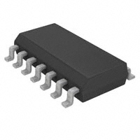
14-Pin Small Outline Package (SOP)
Tape & Reel
© 2009 Fairchild Semiconductor Corporation
FAN6982 • Rev. 1.0.3
www.fairchildsemi.com
FAN6982 — CCM Power Factor Correction Controller
July 2010
�FAN6982 — CCM Power Factor Correction Controller
Application Diagram
Figure 1. Typical Application
© 2009 Fairchild Semiconductor Corporation
FAN6982 • Rev. 1.0.3
www.fairchildsemi.com
2
�14
1
Low-Power
Detect Comparator
FBPFC 2.5V
0.3V
13
6
EN
RM
GmI
2
3
0.5V
PFC UVP
2.75V/2.5V
PFC OVP
VDD
28V/27V
GmV
S
VDD OVP
R
CLR
1.05V/1.9V
VRMS
Q
10
VIN UVP
IM O
Gain Modulator
12
Q
PFC ILIMIT
S
SET
R
CLR
Q
k
2
x
IAC
SET
VREF
OPFC
ISENSE
Range
VDD
7.5V
REFERENCE
-1.15V
VRMS
4
11
IEA
VEA
PGND
VEA
9
Q
RM
2.8V
ISENSE
VDD
UVLO
RDY
5
7
RT/CT
FBPFC
2.4V/1.15V
OSCILLATOR
SGND
8
FAN6982 — CCM Power Factor Correction Controller
Block Diagram
Figure 2. Functional Block Diagram
Marking Information
F – Fairchild Logo
Z – Plant Code
X – 1-Digit Year Code
Y – 1-Digit Week Code
TT – 2-Digit Die-Run Code
T – Package Type (M: SOP)
P – Y: Green Package
M – Manufacture Flow Code
Figure 3. Top Mark
© 2009 Fairchild Semiconductor Corporation
FAN6982 • Rev. 1.0.3
www.fairchildsemi.com
3
�FAN6982 — CCM Power Factor Correction Controller
Pin Configuration
Figure 4. Pin Configuration
Pin Definitions
Pin #
Name
Description
1
IEA
Output of Current Amplifier. This is the output of the PFC current amplifier. The signal from
this pin is compared with sawtooth and determines the pulsewidth for PFC gate drive.
2
IAC
Input AC Current. For normal operation, this input is used to provide current reference for the
multiplier. The suggested maximum IAC is 100µA.
3
ISENSE
4
VRMS
5
RDY
6
EN
7
RT/CT
Oscillator RC Timing Connection. Oscillator timing node; timing set by RT and CT.
8
SGND
Signal Ground.
9
PGND
Power Ground.
10
OPFC
Gate Drive. The totem-pole output drive for PFC MOSFET. This pin is internally clamped
under 15V to protect the MOSFET.
11
VDD
Power Supply. The threshold voltages for startup and turn-off are 11V and 9.3V, respectively.
The operating current is lower than 10mA.
12
VREF
Reference Voltage. Buffered output for the internal 7.5V reference.
13
FBPFC
14
VEA
Current Sense. The non-inverting input of the PFC current amplifier and the output of
multiplier and PFC ILIMIT comparator.
Line-Voltage Detection. The pin is used for PFC multiplier.
Ready Signal. This pin controls the power-on sequence. Once the FAN6982 is turned on and
the FBPFC voltage exceeds in 2.4V, the RDY pin pulls LOW impedance. If the FBPFC voltage
is lower than 1.15V, the RDY pin pulls HIGH impedance.
Enable Range Function. The range function is enabled when EN is connected to VREF.
The range function is disabled when EN is connected to GND.
Voltage Feedback Input. The feedback input for PFC voltage loop. The inverting input of PFC
error amplifier. This pin is connected to the PFC output through a divider network.
Output of Voltage Amplifier. The error-amplifier output for PFC voltage feedback loop.
A compensation network is connected between this pin and ground.
© 2009 Fairchild Semiconductor Corporation
FAN6982 • Rev. 1.0.3
www.fairchildsemi.com
4
�Stresses exceeding the absolute maximum ratings may damage the device. The device may not function or be
operable above the recommended operating conditions and stressing the parts to these levels is not recommended.
In addition, extended exposure to stresses above the recommended operating conditions may affect device
reliability. The absolute maximum ratings are stress ratings only.
Symbol
VDD
Parameter
Min.
DC Supply Voltage
Max.
Unit
30
V
VH
OPFC, RDY, EN, VREF
-0.3
30.0
V
VL
IAC, VRMS, RT/CT, FBPFC, VEA
-0.3
7.0
V
0
VVREF+0.3
V
-5.0
VIEA
IEA
VN
ISENSE
0.7
V
IAC
Input AC Current
1
mA
IREF
VREF Output Current
5
mA
0.5
A
IPFC-OUT
PD
Peak PFC OUT Current, Source or Sink
800
mW
RΘ j-a
Thermal Resistance (Junction-to-Air)
104.10
°C/W
RΘ j-c
Thermal Resistance (Junction-to-Case)
40.61
°C/W
TJ
TSTG
TL
ESD
Power Dissipation, TA < 50°C
Operating Junction Temperature
-40
+125
°C
Storage Temperature Range
-55
+150
°C
+260
°C
Lead Temperature (Soldering)
Electrostatic Discharge Capability
Human Body Model,
JESD22-A114
4.5
Charged Device Model,
JESD22-C101
1.0
FAN6982 — CCM Power Factor Correction Controller
Absolute Maximum Ratings
kV
Notes:
1. All voltage values, except differential voltage, are given with respect to the GND pin.
2. Stresses beyond those listed under Absolute Maximum Ratings may cause permanent damage to the device.
Recommended Operating Conditions
The Recommended Operating Conditions table defines the conditions for actual device operation. Recommended
operating conditions are specified to ensure optimal performance to the datasheet specifications. Fairchild does not
recommend exceeding them or designing to Absolute Maximum Ratings.
Symbol
TA
Parameter
Operating Ambient Temperature
© 2009 Fairchild Semiconductor Corporation
FAN6982 • Rev. 1.0.3
Min.
Max.
Unit
-40
+105
°C
www.fairchildsemi.com
5
�Unless otherwise noted; VDD=15V, TA= 25°C, TA=TJ, RT=27kΩ, and CT=1000pF.
Symbol
Parameter
Conditions
Min.
Typ.
Max.
Units
22
V
30
80
µA
2.0
2.3
3.0
mA
10
11
12
V
1.90
V
29
V
VDD Section
VDD-OP
Continuously Operating
Voltage
IDD ST
Startup Current
VDD=VTH-ON-0.1V; OPFC Open
VDD=13V; OPFC Open
IDD-OP
Operating Current
VTH-ON
Turn-on Threshold Voltage
△VTH
Hysteresis
VDD-OVP
△VDD-OVP
1.35
VDD OVP
27
VDD OVP Hysteresis
28
1
V
Oscillator
fOSC
PFC Frequency
RT=27kΩ, CT=1000pF
(3)
fDV
Voltage Stability
Temperature Stability
fDT
(3)
67
kHz
11V ≦ VDD ≦ 22V
2
%
-40°C ~ +105°C
2
%
70
kHz
fTV
Total Variation
Line, Temperature
fRV
Ramp Voltage
Valley-to-Peak
IOSC-DIS
Discharge Current
VRAMP=0V, VRT/CT=2.5V
fRANGE
Frequency Range
tPFC-DEAD
60
64
58
2.8
V
6.5
15.0
mA
50
75
kHz
PFC Dead Time
RT=27kΩ, CT=1000pF
400
600
800
ns
VVREF
Reference Voltage
IREF=0mA, CREF=0.1µF
7.4
7.5
7.6
V
△VVREF1
Load Regulation of
Reference Voltage
CREF=0.1µF, IREF=0mA to 3.5mA
VVDD=14V, Rise/Fall Time > 20µs
30
50
mV
△VVREF2
Line Regulation of Reference
CREF=0.1µF, VVDD=11V to 22V
Voltage
25
mV
0.5
%
FAN6982 — CCM Power Factor Correction Controller
Electrical Characteristics
VREF
△VVREF-DT
(3)
Temperature Stability
Total Variation
(3)
-40°C ~ +105°C
0.4
Line, Load, Temperature
7.35
7.65
V
Long-Term Stability
TJ=125°C, 0 ~ 1000HRs
5
25
mV
Maximum Current
VVREF > 7.35V
5
VRMS-UVL
VRMS Threshold Low
When VRMS=1.05V at 75 VRMS
1.00
1.05
1.10
V
VRMS-UVH
VRMS Threshold High
When VRMS=1.9V at 85 • 1.414
1.85
1.90
1.95
V
750
850
950
mV
340
410
480
ms
2.3
2.4
2.5
V
1.15
1.25
1.35
V
VFBPFC


 工商网监
湘ICP备2023018690号
工商网监
湘ICP备2023018690号
