ON Semiconductor
Is Now
To learn more about onsemi™, please visit our website at
www.onsemi.com
onsemi and and other names, marks, and brands are registered and/or common law trademarks of Semiconductor Components Industries, LLC dba “onsemi” or its affiliates and/or
subsidiaries in the United States and/or other countries. onsemi owns the rights to a number of patents, trademarks, copyrights, trade secrets, and other intellectual property. A listing of onsemi
product/patent coverage may be accessed at www.onsemi.com/site/pdf/Patent-Marking.pdf. onsemi reserves the right to make changes at any time to any products or information herein, without
notice. The information herein is provided “as-is” and onsemi makes no warranty, representation or guarantee regarding the accuracy of the information, product features, availability, functionality,
or suitability of its products for any particular purpose, nor does onsemi assume any liability arising out of the application or use of any product or circuit, and specifically disclaims any and all
liability, including without limitation special, consequential or incidental damages. Buyer is responsible for its products and applications using onsemi products, including compliance with all laws,
regulations and safety requirements or standards, regardless of any support or applications information provided by onsemi. “Typical” parameters which may be provided in onsemi data sheets and/
or specifications can and do vary in different applications and actual performance may vary over time. All operating parameters, including “Typicals” must be validated for each customer application
by customer’s technical experts. onsemi does not convey any license under any of its intellectual property rights nor the rights of others. onsemi products are not designed, intended, or authorized
for use as a critical component in life support systems or any FDA Class 3 medical devices or medical devices with a same or similar classification in a foreign jurisdiction or any devices intended for
implantation in the human body. Should Buyer purchase or use onsemi products for any such unintended or unauthorized application, Buyer shall indemnify and hold onsemi and its officers, employees,
subsidiaries, affiliates, and distributors harmless against all claims, costs, damages, and expenses, and reasonable attorney fees arising out of, directly or indirectly, any claim of personal injury or death
associated with such unintended or unauthorized use, even if such claim alleges that onsemi was negligent regarding the design or manufacture of the part. onsemi is an Equal Opportunity/Affirmative
Action Employer. This literature is subject to all applicable copyright laws and is not for resale in any manner. Other names and brands may be claimed as the property of others.
�FCD5N60-F085 N-Channel SuperFET® MOSFET
FCD5N60-F085
N-Channel SuperFET® MOSFET
600 V, 4.6 A, 1.1 Ω
Features
600V, 4.6A, typ. Rds(on)=860mΩ@VGS=10V
D
Ultra Low Gate Charge (Typ. Qg = 16 nC)
UIS Capability
RoHS Compliant
D
G
Qualified to AEC Q101
Applications
G
S
Automotive On Board Charger
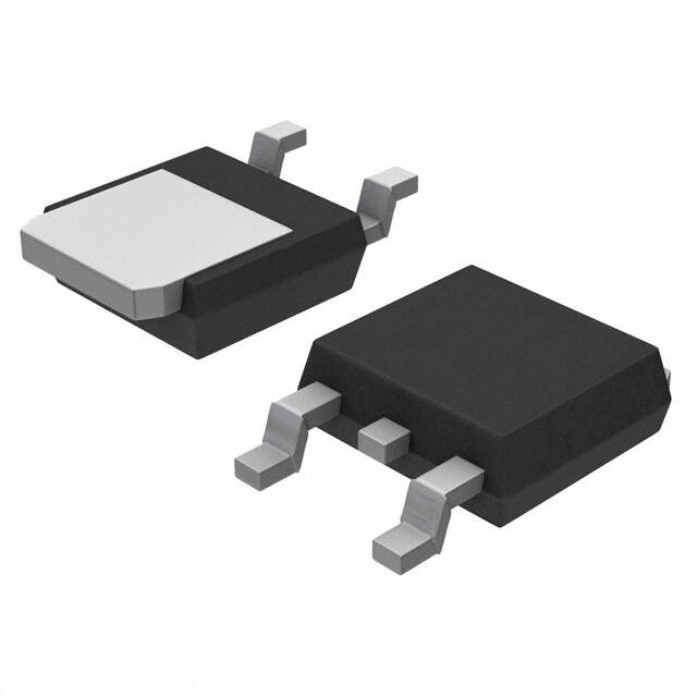
D-PAK
TO-252
(TO-252)
Automotive DC/DC Converter for HEV
S
Description
SuperFETTM is ON Semiconductor proprietary new generation
of high voltage MOSFETs utilizing an advanced charge
balance mechanism for outstanding low on-resistance and
lower gate charge performance.
This advanced technology has been tailored to minimize
conduction loss, provide superior switching performance, and
withstand extreme dv/dt rate and higher avalanche energy.
Consequently, SuperFET is suitable for various automotive DC/DC
power conversion.
MOSFET Maximum Ratings TJ = 25°C unless otherwise noted.
Symbol
VDSS
Drain-to-Source Voltage
VGS
ID
EAS
PD
Parameter
Ratings
600
Units
V
±30
V
Gate-to-Source Voltage
Drain Current - Continuous (VGS=10) (Note 1)
TC = 25°C
4.6
Pulsed Drain Current
TC = 25°C
See Figure 4
Single Pulse Avalanche Energy
(Note 1)
29
Power Dissipation
Derate Above 25oC
TJ, TSTG Operating and Storage Temperature
RθJC
Thermal Resistance, Junction to Case
RθJA
Maximum Thermal Resistance, Junction to Ambient
A
mJ
54
W
1.56
W/oC
-55 to + 150
oC
2.3
oC/W
83
oC/W
(Note 2)
Notes:
1: Starting TJ = 25°C, L = 10mH, IAS = 2.4A, VDD = 100V during inductor charging and VDD = 0V during time in avalanche.
2: RθJA is the sum of the junction-to-case and case-to-ambient thermal resistance, where the case thermal reference is defined as the solder
mounting surface of the drain pins. RθJC is guaranteed by design, while RθJAis determined by the board design. The maximum rating
presented here is based on mounting on a 1 in2 pad of 2oz copper.
Package Marking and Ordering Information
Device Marking
FCD5N60
Device
FCD5N60-F085
©2015 Semiconductor Components Industries, LLC.
August-2017, Rev. 2
Package
D-PAK(TO-252)
Reel Size
13”
Tape Width
16mm
Quantity
2500units
Publication Order Number:
FCD5N60-F085/D
�Symbol
Parameter
Test Conditions
Min.
Typ.
Max.
Units
Off Characteristics
BVDSS
Drain-to-Source Breakdown Voltage
IDSS
Drain-to-Source Leakage Current
IGSS
Gate-to-Source Leakage Current
ID = 250μA, VGS = 0V
600
-
-
V
-
-
1
μA
-
-
10
μA
-
-
±100
nA
VDS=600V, TJ = 25oC
VGS = 0V
TJ = 150oC (Note 4)
VGS = ±30V
On Characteristics
VGS(th)
RDS(on)
Gate to Source Threshold Voltage
Drain to Source On Resistance
VGS = VDS, ID = 250μA
ID = 4.6A,
VGS= 10V
3.0
-
5.0
V
-
0.86
1.1
Ω
-
2.5
3.2
Ω
TJ = 25oC
TJ = 150oC (Note 4)
Dynamic Characteristics
Ciss
Input Capacitance
Coss
Output Capacitance
Crss
Reverse Transfer Capacitance
Rg
Gate Resistance
f = 1MHz
Qg(ToT)
Total Gate Charge
VGS = 0 to 10V
Qg(th)
Threshold Gate Charge
VGS = 0 to 2V
-
1.0
-
nC
Qgs
Gate-to-Source Gate Charge
-
3.2
-
nC
Qgd
Gate-to-Drain “Miller“ Charge
-
7.6
-
nC
ns
VDS = 25V, VGS = 0V,
f = 1MHz
VDD = 480V
ID = 4.6A
-
570
-
pF
-
280
-
pF
-
20
-
pF
-
1.9
-
Ω
-
16
21
nC
Switching Characteristics
ton
Turn-On Time
-
-
84
td(on)
Turn-On Delay
-
18
-
ns
tr
Rise Time
-
19
-
ns
td(off)
Turn-Off Delay
-
48
-
ns
tf
Fall Time
-
13
-
ns
toff
Turn-Off Time
-
-
178
ns
VDD = 300V, ID = 4.6A,
VGS = 10V, RGEN = 25Ω
Drain-Source Diode Characteristics
VSD
Source-to-Drain Diode Voltage
ISD = 4.6A, VGS = 0V
-
-
1.25
V
trr
Reverse-Recovery Time
-
190
250
ns
Qrr
Reverse-Recovery Charge
VDD = 480V, IF = 4.6A,
dISD/dt = 100A/μs
-
1.7
2.2
μC
Note:
4: The maximum value is specified by design at TJ = 150°C. Product is not tested to this condition in production.
www.onsemi.com
2
FCD5N60-F085 N-Channel SuperFET® MOSFET
Electrical Characteristics TJ = 25°C unless otherwise noted.
�1.0
ID, DRAIN CURRENT (A)
POWER DISSIPATION MULTIPLIER
8
1.2
0.8
0.6
0.4
0.2
0.0
0
25
50
75
100
125
TC, CASE TEMPERATURE(oC)
6
4
2
0
150
Figure 1. Normalized Power Dissipation vs. Case
Temperature
VGS = 10V
CURRENT LIMITED
BY PACKAGE
25
50
75
100
125
150
TC, CASE TEMPERATURE(oC)
175
Figure 2. Maximum Continuous Drain Current vs.
Case Temperature
NORMALIZED THERMAL
IMPEDANCE, ZθJC
2
1
0.1
DUTY CYCLE - DESCENDING ORDER
D = 0.50
0.20
0.10
0.05
0.02
0.01
PDM
t1
t2
NOTES:
DUTY FACTOR: D = t1/t2
PEAK TJ = PDM x ZθJA x RθJA + TC
SINGLE PULSE
0.01
-5
10
-4
10
-3
-2
-1
0
10
10
10
t, RECTANGULAR PULSE DURATION(s)
1
10
10
Figure 3. Normalized Maximum Transient Thermal Impedance
100
TC = 25oC
VGS = 10V
FOR TEMPERATURES
IDM, PEAK CURRENT (A)
ABOVE 25oC DERATE PEAK
CURRENT AS FOLLOWS:
150 - TC
I = I2
125
10
SINGLE PULSE
1
-5
10
-4
10
-3
-2
-1
10
10
10
t, RECTANGULAR PULSE DURATION(s)
Figure 4. Peak Current Capability
www.onsemi.com
3
0
10
1
10
FCD5N603F085 N-Channel SuperFET® MOSFET
Typical Characteristics
�10
10us
1
100us
0.1 OPERATION IN THIS
AREA MAY BE
LIMITED BY rDS(on)
0.01
1
1ms
10ms
100ms
SINGLE PULSE
TJ = MAX RATED
TC = 25oC
VGS, GATE TO SOURCE VOLTAGE(V)
ID, DRAIN CURRENT (A)
100
IS, REVERSE DRAIN CURRENT (A)
16
ID, DRAIN CURRENT (A)
VDD = 240V
VDD = 20V
12
8
TJ = 25oC
4
TJ = 150oC
3
TJ = -55oC
4
5
6
7
8
9
VGS, GATE TO SOURCE VOLTAGE (V)
4
2
0
0
8
15V Top
10V
8V
7V
6V
5.5V
5V Bottom
6
4
TJ = 150 oC
1
0.4
TJ = 25 oC
0.6
0.8
1.0
1.2
Figure 8. Forward Diode Characteristics
VGS
8
VGS = 0 V
10
ID, DRAIN CURRENT (A)
10
16
VSD, BODY DIODE FORWARD VOLTAGE (V)
80μs PULSE WIDTH
Tj=25oC
12
4
8
12
Qg, GATE CHARGE(nC)
0.1
0.2
10
Figure 7. Transfer Characteristics
14
VDD = 360V
6
20
PULSE DURATION = 80μs
DUTY CYCLE = 0.5% MAX
VDD =300V
Figure 6. Gate Charge vs. Gate to Source Voltage
20
ID, DRAIN CURRENT (A)
ID = 4.6A
8
10
100
1000 2000
VDS, DRAIN TO SOURCE VOLTAGE (V)
Figure 5. Forward Bias Safe Operating Area
0
10
2
80μs PULSE WIDTH
Tj=150oC
7
6
5
VGS
15V Top
10V
8V
7V
6V
5.5V
5V Bottom
4
3
2
1
0
0
0
4
8
12
16
VDS, DRAIN TO SOURCE VOLTAGE (V)
20
Figure 9. Saturation Characteristics
0
4
8
12
16
VDS, DRAIN TO SOURCE VOLTAGE (V)
Figure 10. Saturation Characteristics
www.onsemi.com
4
20
FCD5N60-F085 N-Channel SuperFET® MOSFET
Typical Characteristics
�ID = 4.6A
5
NORMALIZED
DRAIN TO SOURCE ON-RESISTANCE
rDS(on), DRAIN TO SOURCE
ON-RESISTANCE (Ω)
6
PULSE DURATION = 80μs
DUTY CYCLE = 0.5% MAX
4
3
TJ = 150oC
2
1
TJ = 25oC
0
5
6
7
8
9
VGS, GATE TO SOURCE VOLTAGE (V)
10
Figure 11. RDSON vs. Gate Voltage
2.5
PULSE DURATION = 80μs
DUTY CYCLE = 0.5% MAX
2.0
1.5
1.0
ID = 4.6A
VGS = 10V
0.5
0.0
-80
-40
0
40
80
120
TJ, JUNCTION TEMPERATURE(oC)
1.2
VGS = VDS
ID = 250μA
1.2
ID = 1mA
1.1
1.0
1.0
0.8
0.9
0.6
0.4
-80
-40
0
40
80
120
TJ, JUNCTION TEMPERATURE(oC)
0.8
-80
160
Figure 13. Normalized Gate Threshold Voltage vs.
Temperature
-40
0
40
80
120
TJ, JUNCTION TEMPERATURE (oC)
10000
1000
Ciss
100
Coss
10
f = 1MHz
VGS = 0V
1
0.1
160
Figure 14. Normalized Drain to Source
Breakdown Voltage vs. Junction Temperature
Figure 16.
CAPACITANCE (pF)
160
Figure 12. Normalized RDSON vs. Junction
Temperature
NORMALIZED DRAIN TO SOURCE
BREAKDOWN VOLTAGE
NORMALIZED GATE
THRESHOLD VOLTAGE
1.4
3.0
Crss
1
10
100
1000
VDS, DRAIN TO SOURCE VOLTAGE (V)
Figure 15. Capacitance vs. Drain to Source
Voltage
www.onsemi.com
5
FCD5N60-F085 N-Channel SuperFET® MOSFET
Typical Characteristics
�FCD5N60-F085 N-Channel SuperFET® MOSFET
ON Semiconductor and
are trademarks of Semiconductor Components Industries, LLC dba ON Semiconductor or its subsidiaries in the United States and/or other countries.
ON Semiconductor owns the rights to a number of patents, trademarks, copyrights, trade secrets, and other intellectual property. A listing of ON Semiconductor’s product/patent
coverage may be accessed at www.onsemi.com/site/pdf/Patent−Marking.pdf. ON Semiconductor reserves the right to make changes without further notice to any products herein.
ON Semiconductor makes no warranty, representation or guarantee regarding the suitability of its products for any particular purpose, nor does ON Semiconductor assume any liability
arising out of the application or use of any product or circuit, and specifically disclaims any and all liability, including without limitation special, consequential or incidental damages.
Buyer is responsible for its products and applications using ON Semiconductor products, including compliance with all laws, regulations and safety requirements or standards,
regardless of any support or applications information provided by ON Semiconductor. “Typical” parameters which may be provided in ON Semiconductor data sheets and/or
specifications can and do vary in different applications and actual performance may vary over time. All operating parameters, including “Typicals” must be validated for each customer
application by customer’s technical experts. ON Semiconductor does not convey any license under its patent rights nor the rights of others. ON Semiconductor products are not
designed, intended, or authorized for use as a critical component in life support systems or any FDA Class 3 medical devices or medical devices with a same or similar classification
in a foreign jurisdiction or any devices intended for implantation in the human body. Should Buyer purchase or use ON Semiconductor products for any such unintended or unauthorized
application, Buyer shall indemnify and hold ON Semiconductor and its officers, employees, subsidiaries, affiliates, and distributors harmless against all claims, costs, damages, and
expenses, and reasonable attorney fees arising out of, directly or indirectly, any claim of personal injury or death associated with such unintended or unauthorized use, even if such
claim alleges that ON Semiconductor was negligent regarding the design or manufacture of the part. ON Semiconductor is an Equal Opportunity/Affirmative Action Employer. This
literature is subject to all applicable copyright laws and is not for resale in any manner.
PUBLICATION ORDERING INFORMATION
LITERATURE FULFILLMENT:
Literature Distribution Center for ON Semiconductor
19521 E. 32nd Pkwy, Aurora, Colorado 80011 USA
Phone: 303−675−2175 or 800−344−3860 Toll Free USA/Canada
Fax: 303−675−2176 or 800−344−3867 Toll Free USA/Canada
Email: orderlit@onsemi.com
❖
N. American Technical Support: 800−282−9855 Toll Free
USA/Canada
Europe, Middle East and Africa Technical Support:
Phone: 421 33 790 2910
Japan Customer Focus Center
Phone: 81−3−5817−1050
© Semiconductor Components Industries, LLC
ON Semiconductor Website: www.onsemi.com
Order Literature: http://www.onsemi.com/orderlit
For additional information, please contact your local
Sales Representative
www.onsemi.com
www.onsemi.com
6
�


 工商网监
湘ICP备2023018690号
工商网监
湘ICP备2023018690号
