MOSFET – N-Channel,
SUPERFET) II, FRFET)
650 V, 76 A, 41 mW
FCH041N65F-F085
Description
SuperFET II Mosfet is ON Semiconductor’s brand−new high
voltage super−junction (SJ) MOSFET family that is utilizing charge
balance technology for outstanding low on−resistance and lower gate
charge performance. This technology is tailored to minimize
conduction loss, provide superior switching performance, dv/dt rate
and higher avalanche energy. Consequently, SuperFET II MOSFET is
very well suited for the Soft switching and Hard Switching topologies
like High Voltage Full Bridge and Half Bridge DC−DC, Interleaved
Boost PFC, Boost PFC for HEV−EV automotive.
SuperFET II FRFET MOSFET’s optimized body diode reverse
recovery performance can remove additional component and improve
system reliability.
www.onsemi.com
VDS
RDS(ON) MAX
ID MAX
650 V
41 m� @ 10 V
76 A
D
G
Features
•
•
•
•
•
S
Typ. RDS(on) = 34 m� at VGS = 10 V, ID = 38 A
Typ. Qg(tot) = 234 nC at VGS = 10 V, ID = 38 A
UIS Capability
AEC−Q101 Qualified and PPAP Capable
These Devices are Pb−Free and are RoHS Compliant
N-CHANNEL MOSFET
S
D
G
Applications
• Automotive On Board Charger
• Automotive DC/DC Converter for HEV
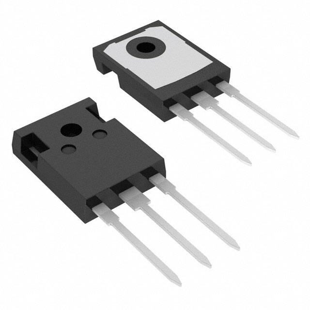
TO−247−3LD
CASE 340CK
MARKING DIAGRAM
$Y&Z&3&K
FCH041N65F
−F085
$Y
&Z
&3
&K
FCH041N65F−F085
= ON Semiconductor Logo
= Assembly Plant Code
= Numeric Date Code
= Lot Code
= Specific Device Code
ORDERING INFORMATION
See detailed ordering and shipping information on page 2 of
this data sheet.
© Semiconductor Components Industries, LLC, 2014
November, 2019 − Rev. 4
1
Publication Order Number:
FCH041N65F−F085/D
�FCH041N65F−F085
ABSOLUTE MAXIMUM RATINGS (TC = 25°C unless otherwise noted)
Symbol
Value
Unit
VDSS
Drain to Source Voltage
650
V
VGSS
Gate to Source Voltage
±20
V
TC = 25°C
76
A
TC = 100°C
48
A
See Fig. 4
A
ID
Parameter
Drain Current − Continuous (VGS = 10)
(Note 1)
Pulsed Drain Current
EAS
Single Pulsed Avalanche Rating (Note 2)
2025
mJ
dv/dt
MOSFET dv/dt
100
V/ns
Peak Diode Recovery dv/dt (Note 3)
50
Power Dissipation
595
W
Derate Above 25°C
4.76
W/°C
−55 to + 150
°C
PD
TJ, TSTG
Operating and Storage Temperature Range
Stresses exceeding those listed in the Maximum Ratings table may damage the device. If any of these limits are exceeded, device functionality
should not be assumed, damage may occur and reliability may be affected.
1. Repetitive rating: pulse−width limited by maximum junction temperature.
2. IAS = 15 A, RG = 25 �, starting TJ = 25 °C.
3. ISD ≤ 38 A, di/dt ≤ 200 A/�s, VDD ≤ 380 V, starting TJ = 25 °C.
PACKAGE MARKING AND ORDERING INFORMATION
Device Marking
Device
Package
Reel Size
Tape Width
Quantity
FCH041N65F
FCH041N65F−F085
TO−247−3
−
−
30 Units
THERMAL CHARACTERISTICS
Symbol
Parameter
R�JC
Thermal Resistance, Junction to Case, Max.
R�JA
Thermal Resistance, Junction to Ambient, Max. (Note 4)
Value
Unit
0.21
°C/W
40
4. R�JA is the sum of the junction−to−case and case−to−ambient thermal resistance, where the case thermal reference is defined as the solder
mounting surface of the drain pins. R�JC is guaranteed by design, while R�JA is determined by the board design. The maximum rating
presented here is based on mounting on a 1 in2 pad of 2oz copper.
www.onsemi.com
2
�FCH041N65F−F085
ELECTRICAL CHARACTERISTICS (TC = 25°C unless otherwise noted)
Symbol
Parameter
Test Condition
Min.
Typ.
Max.
Unit
650
−
−
V
TJ = 25 °C
−
−
10
�A
TJ = 150 °C (Note 5)
−
−
1
mA
VGS = ±20 V
−
−
±100
nA
OFF CHARACTERISTICS
BVDSS
IDSS
IGSS
Drain to Source Breakdown Voltage
ID = 250 �A, VGS = 0 V
Drain to Source Leakage Current
VDS = 650 V,
VGS = 0 V
Gate to Source Leakage Current
ON CHARACTERISTICS
VGS(th)
Gate to Source Threshold Voltage
VGS = VDS, ID = 250 �A
3
−
5
V
RDS(on)
Drain to Source On Resistance
ID = 38 A
VGS = 10 V
TJ = 25 °C
−
34
41
m�
TJ = 150 °C (Note 5)
−
80
96
m�
−
10200
13566
pF
DYNAMIC CHARACTERISTICS
Ciss
Input Capacitance
Coss
Output Capacitance
Crss
Reverse Transfer Capacitance
Coss(eff.)
Effective Output Capacitance
VDS = 25 V, VGS = 0 V,
f = 1 MHz
−
10529
14004
pF
−
227
−
pF
VDS = 0 V to 520 V, VGS = 0 V
−
843
−
pF
Gate Resistance
f = 1 MHz
−
0.5
−
�
Qg(tot)
Total Gate Charge
−
234
304
nC
Qg(th)
Threshold Gate Charge
VDD = 380 V, ID = 38 A,
VGS = 10 V
−
17
22
nC
Rg
Qgs
Gate to Source Gate Charge
−
50
−
nC
Qgd
Gate to Drain “Miller”Charge
−
90
−
nC
−
94
207
ns
−
55
−
ns
SWITCHING CHARACTERISTICS
ton
Turn−On Time
VDD = 380 V, ID = 38 A,
VGS = 10 V, RG = 4.7 �
td(on)
Turn-On Delay Time
tr
Turn−On Rise Time
−
39
−
ns
td(off)
Turn-Off Delay Time
−
183
−
ns
Turn−Off Fall Time
−
8
−
ns
Turn−Off Time
−
191
402
ns
tf
toff
DRAIN-SOURCE DIODE CHARACTERISTICS
Source to Drain Diode Voltage
VGS = 0 V, ISD = 38 A
−
−
1.2
V
trr
Reverse Recovery Time
−
235
−
ns
Qrr
Reverse Recovery Charge
VDD = 480 V, IF = 38 A,
diSD/dt = 100 A/�s
−
2
−
�C
VSD
Product parametric performance is indicated in the Electrical Characteristics for the listed test conditions, unless otherwise noted. Product
performance may not be indicated by the Electrical Characteristics if operated under different conditions.
5. The maximum value is specified by design at TJ = 150°C. Product is not tested to this condition in production.
www.onsemi.com
3
�FCH041N65F−F085
TYPICAL CHARACTERISTICS
100
VGS = 10V
ID, Drain Current (A)
1.0
0.8
0.6
0.4
0.0
80
60
40
20
0.2
0
25
50
75
100
125
0
150
25
75
100
125
150
Figure 2. Maximum Continuous Drain Current vs.
Case Temperature
Figure 1. Normalized Power Dissipation vs.
Case Temperature
Normalized Thermal Impedance, Z�JC
50
TC, Case Temperature (°C)
TC, Case Temperature (°C)
2
DUTY CYCLE − DESCENDING ORDER
1
D = 0.50
0.20
0.10
0.05
0.02
0.01
0.1
PDM
t1
t2
NOTES:
DUTY FACTOR: D = t 1/t 2
PEAK T J = PDM x Z �JC x R �JC + TC
SINGLE PULSE
0.01
−5
10
−4
−3
10
10
−2
−1
10
10
t, Rectangular Pulse Duration(s)
Figure 3. Normalized Maximum Transient Thermal Impedance
10000
T C = 25 o C
VGS = 10V
FOR TEMPERA TURES
ABOVE 25 o C DERAT E PEAK
IDM, Peak Current (A)
Power Dissipation Multiplier
1.2
1000
CURRE NT AS FOLLOWS:
I = I2
150 − T C
12 5
100
10
1
−5
10
SINGLE PULSE
−4
−3
10
10
t, Rectangular Pulse Duration(s)
Figure 4. Peak Current Capability
www.onsemi.com
4
−2
10
−1
10
�FCH041N65F−F085
TYPICAL CHARACTERISTICS
200
100
ID, Drain Current (A)
ID, Drain Current (A)
1000
10us
10
100us
OPERATION IN THIS
AREA MAY BE
LIMITED BY R DS(on)
1
1ms
SINGLE PULSE
TJ = MAX RATED
10ms
TC = 25 oC
100ms
10
100
160
VDS = 20V
120
TJ = 150oC
80
TJ = 25oC
40
TJ = −55o C
0.1
1
PULSE DURATION = 80� s
DUTY CYCLE = 0.5% MAX
0
1000
345678
VDS, Drain to Source Voltage (V)
Figure 6. Transfer Characteristics
Figure 5. Forward Bias Safe Operating Area
200
VGS = 0 V
TJ =
ID, Drain Current (A)
IS, Reverse Drain Current (A)
200
100
150 oC
10
TJ = 25 oC
TJ = −55oC
1
0.1
0.0
0.2
0.4
0.6
0.8
1.0
160
VGS
15 V Top
10 V
8V
7V
6V
5.5 V
5 V Bottom
120
80
40
0
1.2
80 �s PULSE WIDTH
TJ = 25°C
5V
0
4
RDS(on), Drain to Source On−Resistance (m�)
ID, Drain Current (A)
80 �s PULSE WIDTH
TJ = 150°C
VGS
15 V Top
10 V
8V
7V
6V
5.5 V
5 V Bottom
80
40
5V
0
0
4
8
12
16
12
16
20
Figure 8. Saturation Characteristics
Figure 7. Forward Diode Characteristics
120
8
VDS, Drain to Source Voltage (V)
VSD, Body Diode Forward Voltage (V)
160
VGS, Gate to Source Voltage (V)
20
VDS, Drain to Source Voltage (V)
250
PULSE DURATION = 80 �s
DUTY CYCLE = 0.5% MAX
ID = 38A
200
150
100
TJ = 150oC
50
o
0
TJ = 25 C
4
5
6
7
8
9
10
VGS, Gate to Source Voltage (V)
Figure 10. RDSON vs. Gate Voltage
Figure 9. Saturation Characteristics
www.onsemi.com
5
�FCH041N65F−F085
3.0
PULSE DURATION = 80 � s
DUTY CYCLE = 0.5% MAX
2.5
2.0
1.5
1.0
ID = 38A
VGS = 10V
0.5
0.0
−80
−40
0
40
80
120
160
200
VGS = VDS
ID = 250 �A
1.1
1.0
0.9
0.8
0.7
0.6
0.5
−80
−40
TJ, Junction Temperature (°C)
0
40
80
120
160
200
TJ, Junction Temperature (°C)
Figure 12. Normalized Gate Threshold Voltage vs.
Temperature
Figure 11. Normalized RDSON vs. Junction
Temperature
1.10
100000
ID = 10mA
1.05
Capacitance (pF)
Normalized Drain to Source Breakdown Voltage
1.2
Normalized Gate Threshold Voltage
Normalized Drain to Source On−Resistance
TYPICAL CHARACTERISTICS
1.00
0.95
Ciss
10000
1000
Coss
100
10
0.90
−75 −50 −25
0
25
50
f = 1MHz
VGS = 0V
1
0.1
75 100 125 150
TJ, Junction Temperature (°C)
Crss
1
10
100
1000
VDS, Drain to Source Voltage (V)
Figure 14. Capacitance vs. Drain to Source
Voltage
Figure 13. Normalized Drain to Source Breakdown
Voltage vs. Junction Temperature
54.0
ID = 38 A
8
43.2
VDS = 260V
VDS = 325V
Eoss, (�J)
VGS, Gate to Source Voltage (V)
10
VDS = 390V
6
4
21.6
10.8
2
0
32.4
0
40
80
120
160
200
0
240
0
132
264
396
528
660
VDS, Drain to Source Voltage (V)
Qg, Gate Charge (nC)
Figure 16. Eoss vs. Drain to Source Voltage
Figure 15. Gate Charge vs. Gate to Source
Voltage
www.onsemi.com
6
�FCH041N65F−F085
VGS
RL
Qg
VDS
VGS
Qgs
Qgd
DUT
IG = Const.
Charge
Figure 17. Gate Charge Test Circuit & Waveform
RL
VDS
VDS
90%
90%
90%
VDD
VGS
RG
VGS
DUT
VGS
10%
td(on)
10%
tr
tf
td(off)
ton
toff
Figure 18. Resistive Switching Test Circuit & Waveforms
L
E AS + 1 @ LI AS
2
VDS
BVDSS
ID
IAS
RG
VDD
DUT
VGS
2
ID(t)
VDD
VDS(t)
tp
tp
Figure 19. Unclamped Inductive Switching Test Circuit & Waveforms
www.onsemi.com
7
Time
�FCH041N65F−F085
+
DUT
VSD
−
ISD
L
Driver
RG
Same Type
as DUT
VGS
− dv/dt controlled by RG
− ISD controlled by pulse period
D+
VGS
(Driver)
VDD
Gate Pulse Width
Gate Pulse Period
10 V
IFM, Body Diode Forward Current
ISD
(DUT)
di/dt
IRM
Body Diode Reverse Current
Body Diode Recovery dv/dt
VDS
(DUT)
VDD
VSD
Body Diode
Forward Voltage Drop
Figure 20. Peak Diode Recovery dv/dt Test Circuit & Waveforms
SUPERFET is a registered trademark of Semiconductor Components Industries, LLC (SCILLC) or its subsidiaries in the United States and/or
other countries.
FRFET is a registered trademark of Semiconductor Components Industries, LLC (SCILLC) or its subsidiaries in the United States and/or other
countries.
www.onsemi.com
8
�MECHANICAL CASE OUTLINE
PACKAGE DIMENSIONS
TO−247−3LD SHORT LEAD
CASE 340CK
ISSUE A
A
DATE 31 JAN 2019
A
E
P1
P
A2
D2
Q
E2
S
B
D
1
2
D1
E1
2
3
L1
A1
L
b4
c
(3X) b
0.25 M
(2X) b2
B A M
DIM
(2X) e
GENERIC
MARKING DIAGRAM*
AYWWZZ
XXXXXXX
XXXXXXX
XXXX = Specific Device Code
A
= Assembly Location
Y
= Year
WW = Work Week
ZZ
= Assembly Lot Code
*This information is generic. Please refer to
device data sheet for actual part marking.
Pb−Free indicator, “G” or microdot “G”, may
or may not be present. Some products may
not follow the Generic Marking.
DOCUMENT NUMBER:
DESCRIPTION:
98AON13851G
TO−247−3LD SHORT LEAD
A
A1
A2
b
b2
b4
c
D
D1
D2
E
E1
E2
e
L
L1
P
P1
Q
S
MILLIMETERS
MIN NOM MAX
4.58 4.70 4.82
2.20 2.40 2.60
1.40 1.50 1.60
1.17 1.26 1.35
1.53 1.65 1.77
2.42 2.54 2.66
0.51 0.61 0.71
20.32 20.57 20.82
13.08
~
~
0.51 0.93 1.35
15.37 15.62 15.87
12.81
~
~
4.96 5.08 5.20
~
5.56
~
15.75 16.00 16.25
3.69 3.81 3.93
3.51 3.58 3.65
6.60 6.80 7.00
5.34 5.46 5.58
5.34 5.46 5.58
Electronic versions are uncontrolled except when accessed directly from the Document Repository.
Printed versions are uncontrolled except when stamped “CONTROLLED COPY” in red.
PAGE 1 OF 1
ON Semiconductor and
are trademarks of Semiconductor Components Industries, LLC dba ON Semiconductor or its subsidiaries in the United States and/or other countries.
ON Semiconductor reserves the right to make changes without further notice to any products herein. ON Semiconductor makes no warranty, representation or guarantee regarding
the suitability of its products for any particular purpose, nor does ON Semiconductor assume any liability arising out of the application or use of any product or circuit, and specifically
disclaims any and all liability, including without limitation special, consequential or incidental damages. ON Semiconductor does not convey any license under its patent rights nor the
rights of others.
© Semiconductor Components Industries, LLC, 2018
www.onsemi.com
�onsemi,
, and other names, marks, and brands are registered and/or common law trademarks of Semiconductor Components Industries, LLC dba “onsemi” or its affiliates
and/or subsidiaries in the United States and/or other countries. onsemi owns the rights to a number of patents, trademarks, copyrights, trade secrets, and other intellectual property.
A listing of onsemi’s product/patent coverage may be accessed at www.onsemi.com/site/pdf/Patent−Marking.pdf. onsemi reserves the right to make changes at any time to any
products or information herein, without notice. The information herein is provided “as−is” and onsemi makes no warranty, representation or guarantee regarding the accuracy of the
information, product features, availability, functionality, or suitability of its products for any particular purpose, nor does onsemi assume any liability arising out of the application or use
of any product or circuit, and specifically disclaims any and all liability, including without limitation special, consequential or incidental damages. Buyer is responsible for its products
and applications using onsemi products, including compliance with all laws, regulations and safety requirements or standards, regardless of any support or applications information
provided by onsemi. “Typical” parameters which may be provided in onsemi data sheets and/or specifications can and do vary in different applications and actual performance may
vary over time. All operating parameters, including “Typicals” must be validated for each customer application by customer’s technical experts. onsemi does not convey any license
under any of its intellectual property rights nor the rights of others. onsemi products are not designed, intended, or authorized for use as a critical component in life support systems
or any FDA Class 3 medical devices or medical devices with a same or similar classification in a foreign jurisdiction or any devices intended for implantation in the human body. Should
Buyer purchase or use onsemi products for any such unintended or unauthorized application, Buyer shall indemnify and hold onsemi and its officers, employees, subsidiaries, affiliates,
and distributors harmless against all claims, costs, damages, and expenses, and reasonable attorney fees arising out of, directly or indirectly, any claim of personal injury or death
associated with such unintended or unauthorized use, even if such claim alleges that onsemi was negligent regarding the design or manufacture of the part. onsemi is an Equal
Opportunity/Affirmative Action Employer. This literature is subject to all applicable copyright laws and is not for resale in any manner.
PUBLICATION ORDERING INFORMATION
LITERATURE FULFILLMENT:
Email Requests to: orderlit@onsemi.com
onsemi Website: www.onsemi.com
◊
TECHNICAL SUPPORT
North American Technical Support:
Voice Mail: 1 800−282−9855 Toll Free USA/Canada
Phone: 011 421 33 790 2910
Europe, Middle East and Africa Technical Support:
Phone: 00421 33 790 2910
For additional information, please contact your local Sales Representative
�